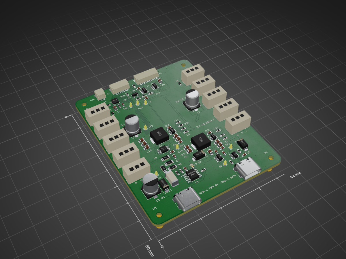
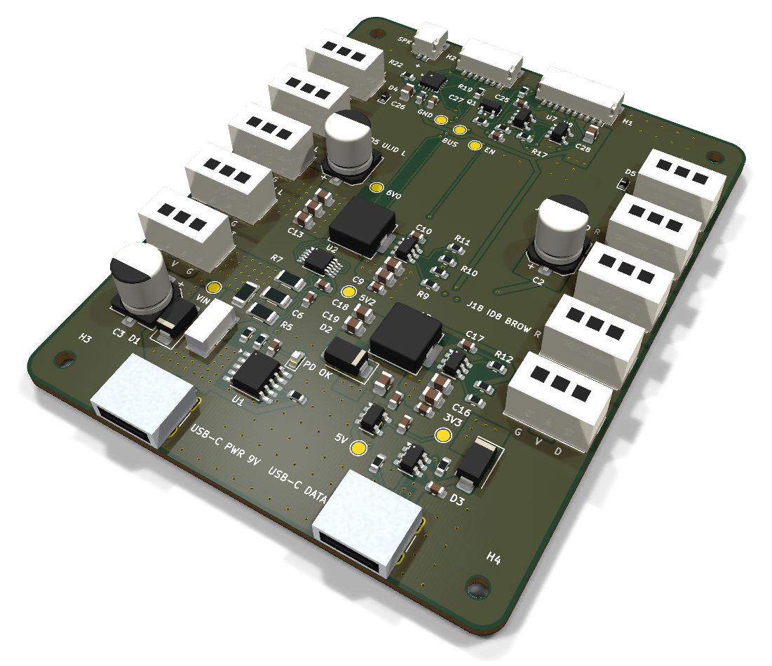
Iris Brainstem: power and servo hub of the Iris robot head. 9 V USB-C PD in, 6 V / 5 A servo rail in stitched copper zones (measured), 5 V rail, half-duplex servo bus with ten ports, speaker amp. 4-layer KiCad 10 board, DRC-clean, fab-ready.
Iris brainstem is an open-source printed circuit board by HeyPCB, from the HeyPCB/iris-brainstem repository on GitHub, published under the CERN-OHL-S-2.0 licence. It is a 4-layer board of 64 × 80 mm with 97 parts on 59 nets, routed with 770 tracks and 208 vias.
It is built around the SN74LVC1G125DBVR-TP, SN74LVC1G126DBVR-TP and CH224K, with the INA226AIDGSR, MAX98357AETE+T and TPS56339DDC among its other parts. Its parts include 28 capacitors, 22 resistors, 15 connectors, 9 ICs and 6 diodes. It belongs with the robots and motor control and audio and music boards of this library.
The power and servo hub in the base of Iris: 9 V USB-C PD in, a 6 V / 5 A servo rail laid in stitched copper zones, a 5 V rail, the half-duplex servo bus with ten ports, a speaker amp and a USB-C data port.
Part of Iris, the human-eyed robot head, HeyPCB's open robot boards. Designed end to end with the HeyPCB method on
KiCad 10 (headless pipeline, Freerouting 2.4.1); every number below is measured on the files in this repository.
Mentions of ./run.sh, docs/rules/, blocks/ or parts/ refer to the heypcb-kicad SDK that produced them.
Iris Brainstem is board B2 of Iris, a robot head with human-like eyes. It sits flat in the base of
the head and is the head's power, USB and servo hub. It takes 9 V from a USB-C PD charger, makes a
6.0 V / 5 A rail for the ten eye, lid and brow servos and a 5 V rail for the head controller (B1
Cortex), measures the input with an INA226, drives the servos' half-duplex serial bus and the
speaker, and passes a second USB-C port's data up to B1. It was designed with the HeyPCB method on
KiCad 10 (10.0.6), by heypcb-kicad's headless pipeline with Freerouting 2.4.1, from the brief in
board.json and section 4.2 of the Iris design spec v0.1 (not published; its binding interconnect and mounting
contracts are in the Iris system docs).
This board has not been fabricated, assembled or powered, and no firmware for it has been
written. Everything below is what KiCad, the pipeline and the copper scripts measured on the
design files. Nothing here has been tested on hardware or in the head.
Role in Iris
Iris has four boards (spec 4): B1 Cortex (ESP32-S3, camera, on the eye cradle), B2
Brainstem (this board, in the head's base), B3 Iris ring (two LED rings) and B4 Brow
(forehead sensors). B2 is where power enters the head and where every servo plugs in:
USB-C J1 PWR brings 9 V. Everything in the head is powered from here.
USB-C J2 DATA carries a PC's USB to B1's native USB, and its VBUS powers the logic on its own
(servos stay off).
H1 (JST SH-10) and H2 (JST SH-7) are the two harnesses to B1: 5V_SYS, USB, the servo bus
and SERVO_EN on H1; I2C, the INA226's alert and I2S audio on H2 (spec 5).
J10-J19 are the servo ports, J7 the speaker.
Features
USB-C PD sink, 9 V, no firmware. WCH CH224K (U1) with CFG1, CFG2 and CFG3 tied straight to
GND, which requests 9 V. There is no configuration resistor to go missing: on the CH224K a
missing resistor on CFG1 would request 20 V. VDD through 1 kOhm with 1 uF, VBUS sense through
10 kOhm (WCH's reference schematic). A red PD OK LED (D6) hangs on the CH224K's PG output
(open drain, active low).
Input protection and measurement. SMAJ15A TVS (D1), 5 A Littelfuse NANO2 fuse (F1,
0451005.MRL), 10 mOhm 1206 shunt (R1) read by an INA226 at 0x40 (U2, ALERT on H2 pin 4), and
470 uF on VIN (C3).
6V0_SERVO, 5 A. TPS565208 buck (U3) to 5.93 V (68 k / 10 k on a 0.760 V reference), 3.3 uH
FXL0630, 3 x 22 uF at the regulator and 470 uF at each servo bank (C1, C2). Off by default:
EN is SERVO_EN from B1 through 1 kOhm with a 100 kOhm pull-down.
5V2 and 5V_SYS. TPS56339 buck (U4) to 5.21 V (54.9 k / 10 k on 0.802 V), 5.6 uH FXL0630, then
an SS34 (D2) onto 5V_SYS. J2's VBUS joins 5V_SYS through a second SS34 (D3). Neither VBUS is
ever driven by the board. 5V_SYS goes to B1 on H1 pins 1-2 and to the amplifier.
3V3_B2. AP2112K-3.3 (U6) from 5V_SYS for the INA226, the bus buffers and their pull-ups.
Servo bus. The Waveshare / Feetech auto-direction half-duplex driver: 74LVC1G126 (U7),
74LVC1G125 (U8) and an MMBT3906 (Q1), 10 k pull-ups on BUS_TX, BUS_RX and BUS_DATA, an ESD5Z5.0 on
BUS_DATA at each bank (D4, D5). TX is never echoed back to RX.
Ten servo ports (J10-J19), HC-5264-3A vertical (Molex 5264 type), pin 1 BUS_DATA, pin 2
6V0_SERVO, pin 3 GND, in two banks of five down the left and right edges. D V G is printed at
every port and each port is labelled with its servo ID.
Speaker amplifier. MAX98357A (U9) on B1's I2S, mono (L+R)/2 (1 MOhm on SD_MODE), 9 dB gain,
from 5V_SYS through a ferrite, to a JST SH-2 (J7). Bridge-tied output: neither wire is ground.
USB data port. J2 with 5.1 kOhm on CC1 and CC2 (a plain sink) and a USBLC6-2SC6 (U5) on D+ /
D- before H1.
Test pads (1.5 mm, not fitted parts): VIN, 6V0, 5V2, 5V_SYS, 3V3_B2, BUS_DATA, SERVO_EN and
GND (TP1-TP8).
Board: 64.0 x 80.0 mm, corner fillet 3.0 mm, 1.6 mm, 4 copper layers: F.Cu signal and power
zones, In1 a solid GND plane, In2 signal with a 6V0_SERVO pour, B.Cu mostly a power layer
(6V0_SERVO, VIN and 5V_SYS zones, with keep-outs that hold signal tracks off them; 101.5 mm of
track runs on B.Cu elsewhere). Every part is on the top side. Four non-plated 2.2 mm holes for
M2 screws.
The input enters at the rear left (J1), and F1, R1 and C3 stand in one column above it. The servo
buck sits in the middle of the board, with its output node (L1, three 22 uF and C1) on the left,
and the ten ports run down both side edges. The 5V2 buck and the two diodes are at the rear right,
beside J2.
Load figures (spec 6, all estimates, none measured): VIN 0.68 A typical, about 4.3 A for
milliseconds (39 W); 6V0_SERVO 0.58 A typical, a 7-servo burst of 4.6 A for milliseconds, 9 A if
every servo stalls (beyond the buck's 5 A by design: firmware must cut torque); 5V_SYS 0.41 A
typical, 1.56 A peak. A 27 W (9 V, 3 A) PD charger is the spec's supply.
Net classes (from the brief; a class with a current is never narrowed by the routing ladder):
PDIN 0.6 mm (VBUS_PD, VIN_F, VIN; 0.6 mm is the receptacle's VBUS pads and the bucks' VIN pins),
SERVO 0.8 mm with 0.8 / 0.4 mm vias (6V0_SERVO), SWNODE 0.6 mm (the two switch nodes), RAIL5V
0.6 mm (5V2, 5V_SYS), USBVBUS 0.6 mm (VBUS_DATA). The tracks only connect the path. The current is
carried by the zones below.
Power zones
After routing reaches 0 open, the pour stage lays the plan pours (GND on F.Cu, B.Cu and In1,
6V0_SERVO on In2) and then the brief's board.zones: each a named net's copper over a region on
chosen layers, above the plan pours, with every pad joined solid, and where the zone has a
stitch pitch, its own 0.6 / 0.3 mm via lattice. Board coordinates are mm from the outline's
top-left corner (y = 0 is the front edge). Every reason is also in board.json.
Zone
Net
Layers
Region
Priority
Vias placed
vbus_pd
VBUS_PD
F.Cu, B.Cu
J1's VBUS pads, D1's cathode, F1's input pad (x 9.6-21.6, y 64.4-71.7)
1
20 at 1.2 mm
vin_f
VIN_F
F.Cu
F1's output pad to R1, and the INA226's IN+ resistor (x 14.6-19.7, y 57.6-62.7)
2
-
vin_col
VIN
F.Cu, B.Cu
R1's VIN pad, C3's + pad, the INA226's IN- / VBUS taps (polygon in x 5.4-19.7, y 51.6-63.4)
3
27 at 1.2 mm
vin_band
VIN
B.Cu
from the input column to both buck inputs (x 9.6-44.8, y 44.9-57.4)
2
-
vin_u3, vin_u4
VIN
F.Cu, B.Cu
each buck's VIN pin and input capacitors
10
4 and 5 at 1.2 mm
v6_b
6V0_SERVO
B.Cu
a U: the left bank strip, a bar along the front (y 7.3-12.5), the right bank strip
5
-
v6_node
6V0_SERVO
F.Cu, B.Cu
L1's output pad, the three 22 uF and C1 (x 14.6-23.0, y 31.6-44.7)
6
8 at 1.2 mm
v6_bank_l, v6_bank_r, v6_c2
6V0_SERVO
F.Cu
the V pins of each bank (x 4.6-7.45 and 56.55-59.4, y 12.5-57.0) and C2
7, 8
-
gnd_out6, gnd_in6, gnd_in5
GND
F.Cu
the GND sides of the servo buck's output and input capacitors and of the 5V2 buck's input
9
12, 5 and 0 at 1.2 mm
gnd_front, gnd_mid, gnd_rear
GND
F.Cu, B.Cu
the front strip, the middle and the rear right, where the plan pour would otherwise have no vias
0
16, 21 and 51 at 2.4 mm
v5_spine
5V_SYS
B.Cu
from D2 / D3 at the rear, up the right of the middle (x 45.4-50.8) to H1
12
-
v5_front, v5_link_*
5V_SYS
F.Cu (+ B.Cu)
H1's pins 1-2, and the three places the spine meets F.Cu (D2, D3, H1)
12, 13
3, 5 and 3 at 1.2 mm
sw_6v0, sw_5v2
SW_6V0, SW_5V2
F.Cu
the gap between each buck's SW pin and its inductor
11
-
v5v2_out
5V2
F.Cu
L2's output pad, the two 22 uF and D2's anode (polygon in x 30.4-36.6, y 51.6-60.4), left of VIN's F.Cu track to U4
14
-
B.Cu is kept free of signal tracks under these zones by seven board.keepouts rectangles
(bcu_*), and In2 is kept free of tracks where the VBUS_PD, VIN and the servo buck's via fields
need room (in2_*): a stitch via must clear other nets' tracks on every layer. gnd_in5 found no
via site (U4's GND pins reach In1 through the plan's own vias). Any GND zone stops the plan's GND
stitcher, so the plan's stitching count is 0 and the GND zones stitch themselves. The silkscreen
then displaced 25 GND stitching vias under its text, which leaves 208 vias on the board (read
off the board: 206 of 0.6 / 0.3 mm and 2 of 0.8 / 0.4 mm; 53 of them are routing vias).
Measured copper on the current path
copper.py (KiCad's Python) lists every track, via and pour of each power net on the final board
and exports the copper (tracks, pads, plan pours and zones) as polygons. copper_cut.py (any
Python with numpy and scipy) rasterises that copper on a 0.1 mm grid and finds, for each link of
the path, the narrowest cross-section the link's whole current must pass: a max-flow / min-cut
from the link's source pads to its sink pads, over every layer, with tracks, zones and via barrels
together, in parallel. Outer copper is taken as 35 um, inner as 17.5 um (JLCPCB's standard 4-layer
build), via plating as 25 um. Each cut is rated with heypcb_kicad.route.ipc2221_amps (IPC-2221,
I = k dT^0.44 A^0.725), per layer, summed. Each link is cut a second time with the copper within
1 mm of its pads counted as the pads ("beyond the pads"): that rates the board's own copper between
the parts, apart from the parts' fixed lands. Both scripts are copies of quack_core's, adapted.
Link
From, to
Narrowest cross-section (35 um equivalent)
10 C rise
20 C rise
Beyond the pads, 10 C / 20 C
VBUS_PD
J1 VBUS pads (A4, A9, B4, B9) to F1.1
1.15 mm of F.Cu, at the receptacle's VBUS pads
2.6 A
3.6 A
9.0 A / 12.2 A (6.23 mm)
VIN_F
F1.2 to R1.1
4.24 mm of F.Cu
6.8 A
9.2 A
pads adjacent
VIN, both bucks
R1.2 to U3 and U4 VIN pins and their input capacitors
5.09 mm of F.Cu
7.8 A
10.6 A
9.3 A / 12.6 A (In2 0.25, barrels 6.06)
VIN, servo buck
R1.2 to U3.3, C7.1, C8.1
3.08 mm: In2 0.39, 4 via barrels 2.69
5.5 A
7.5 A
5.5 A / 7.5 A
SW_6V0
U3.2 to L1.1
0.80 mm of F.Cu: U3's SW pin
2.0 A
2.8 A
pads adjacent
6V0_SERVO, all ports
L1.2 to J10-J19 pin 2
6.09 mm: F.Cu 0.70, 8 via barrels 5.39
10.0 A
13.5 A
10.0 A / 13.5 A
6V0_SERVO, each bank
L1.2 (with C11-C13, C1) to J10-J14 or J15-J19 pin 2
6.09 mm, the same section
10.0 A
13.5 A
10.0 A / 13.5 A
6V0_SERVO, bank to bank
J10-J14 pin 2 to J15-J19 pin 2
7.61 mm: In2 2.82, B.Cu 4.78
10.0 A
13.5 A
13.4 A / 18.2 A
GND, ports to servo buck
J10-J19 pin 3 to U3.1, C11-C13 pin 2
8.63 mm of F.Cu
11.4 A
15.5 A
13.3 A / 18.0 A
GND, servo buck to input
U3.1, C7.2, C8.2 to J1 GND pads
2.97 mm of F.Cu
5.3 A
7.1 A
13.4 A / 18.2 A (F.Cu 5.74, barrels 2.69)
5V2
L2.2 to D2.2 (anode)
1.04 mm of F.Cu
2.5 A
3.3 A
2.5 A / 3.3 A
5V_SYS
D2.1, D3.1 (cathodes) to J5 pins 1-2
0.99 mm of F.Cu
2.4 A
3.2 A
2.4 A / 3.2 A
Read off the board (copper_cut.json, copper.json) after the full run with
media. "Pads adjacent" means the two terminals are within 2 mm of each other, so the link is the
pads' own gap.
What this says against spec 6. At a 10 C rise on 1 oz outer copper:
The servo rail has about twice the copper its burst needs. 6V0_SERVO from L1 to the ports
rates 10.0 A (13.5 A at 20 C) against the 4.6 A burst and the buck's 5 A limit. The narrowest
section is at L1's output node, where the F.Cu node meets the eight vias of v6_node; past that
the current spreads over the B.Cu U, the In2 pour and the F.Cu bank strips. The GND return from
the ports to the buck's output capacitors rates 11.4 A.
The input path carries the 4.3 A peak at a 10 C rise on every board-copper link: VIN_F
6.8 A, VIN to both bucks 7.8 A, VIN to the servo buck 5.5 A, the GND return from the buck input
to J1 5.3 A (13.4 A beyond the pads).
Two links end on a part's own pins and rate lower by this rule. VBUS_PD leaves the
receptacle through its VBUS pads: 1.15 mm of copper at the pads' edges, 2.6 A at 10 C and 3.6 A
at 20 C, against the 3 A PD contract and the millisecond 4.3 A peaks. Beyond the pads the zone
is 6.23 mm (9.0 A). SW_6V0 is the TPS565208's 0.8 mm SW pin, 2.0 A by the chart against a 5 A
switch current. Both are lands fixed by the footprint and well under 2 mm long; IPC-2221's chart
is for long conductors, so these figures say little about the real limit, and neither was
measured. The receptacle's current rating was not checked (see Check before ordering).
5V2 and 5V_SYS rate 2.5 A and 2.4 A (3.3 A and 3.2 A at 20 C) against the 1.56 A peak.
H1's two 5V_SYS pins are JST SH contacts rated 1 A each (catalogue rows), 2 A together, which
the spec's 1.6 A respects.
Via barrels are rated with the same formula as a plated wall; that is an approximation.
Nothing here is a measured temperature. Measure F1, R1, J1, U3, L1 and the port headers under the
real servo load before trusting any of it. The routed widths of the rest of the power nets, read
off the board: VBUS_DATA 0.6 mm (0.45 mm necks at pads, 2 vias), SW_5V2 0.6 mm plus its zone,
VIN's routed tracks 0.6 mm.
Connectors and pinouts
Every connector follows spec 5 (binding). "Pin n" is pad n of the KiCad footprint. Both harness
cables are double-ended, same direction (pin n to pin n), 28 AWG, 150 mm. The SH headers are
side-entry with their mouths at the front edge; the board's header pin counts (10, 7, 2) all
differ, so no cable fits a wrong header.
H1: J5, JST SH-10 (SM10B-SRSS-TB, C160409) to B1 J5
Pin
Net
Direction
Level / type
Notes
1
5V_SYS
B2 -> B1
4.85 V nominal (5V2 - SS34), <= 1.6 A total on pins 1-2
source B2
2
5V_SYS
B2 -> B1
as pin 1
3
GND
-
4
GND
-
5
USB_DN
both
USB 2.0 FS D-, 90 Ohm pair with 6
ESD on B2 (U5); B1 GPIO19
6
USB_DP
both
USB 2.0 FS D+
B1 GPIO20
7
GND
-
separates the USB pair from the UART
8
BUS_TX
B1 -> B2
3.3 V UART, 1 Mbps, 8N1, idle high
B1 GPIO42 -> U7 A + Q1 base network (10 k pull-up on B2)
9
BUS_RX
B2 -> B1
3.3 V UART
U8 Y -> B1 GPIO44; 10 k pull-up on B2
10
SERVO_EN
B1 -> B2
3.3 V CMOS, active high
-> U3 EN via 1 k; 100 k pull-down on B2
The board's nets carry the spec's names (USB_DN, USB_DP, BUS_TX and so on). The USB pair is routed
as two plain signals, without an impedance class (USB full speed). The mounting tabs are grounded.
H2: J6, JST SH-7 (SM07B-SRSS-TB, C160406) to B1 J6
Pin
Net
Direction
Level / type
Notes
1
GND
-
2
I2C_SDA
both
3.3 V open drain, 400 kHz
pull-ups 2.2 k on B1 only (none on B2)
3
I2C_SCL
B1 ->
3.3 V open drain
4
nINT
B2 -> B1
open drain, active low
INA226 ALERT; 10 k pull-up on B1 (GPIO3)
5
I2S_BCLK
B1 -> B2
3.3 V, 3.072 MHz (48 kHz x 64)
33 Ohm series at B1; -> U9 BCLK
6
I2S_WS
B1 -> B2
3.3 V, 48 kHz
33 Ohm series at B1; -> U9 LRCLK
7
I2S_AMP_SD
B1 -> B2
3.3 V I2S data
-> U9 DIN
The mounting tabs are grounded.
SPK: J7, JST SH-2 (SM02B-SRSS-TB, C160402)
Pin 1 OUTP (SPK_P, marked "+" on the silkscreen), pin 2 OUTN (SPK_N). A bridge-tied load:
neither wire is ground. 4-8 Ohm, about 1 W speaker (spec 5). The mounting tabs are grounded.
USB-C: J1 PWR and J2 DATA (HRO TYPE-C-31-M-12, C165948)
J1 PWR. CC1 / CC2 to the CH224K; VBUS to D1 and F1; D+ / D- to the CH224K's DP / DM (BC1.2
only, not to B1).
J2 DATA. CC1 / CC2 each 5.1 kOhm to GND; D+ / D- through U5 to H1 pins 6 / 5; VBUS through D3
to 5V_SYS. The board never drives this VBUS.
J2 only (a PC): logic runs, servos stay off (VIN reads 0 V). J1 only: everything runs,
with no USB data. Both: 5V_SYS takes the higher of 5V2 and J2's VBUS, each through its own
SS34.
3.3 V half-duplex, 1 Mbps; 10 k pull-up to 3V3_B2; ESD5Z5.0 at each bank
2
6V0_SERVO
V
source B2 (U3); at most 1 A per port (stall)
3
GND
G
Watch the numbering: Feetech numbers the servo's own plug "1 GND, 2 Vcc, 3 Signal"; Waveshare
numbers the mating header "1 DATA, 2 VCC, 3 GND". The board follows Waveshare (pad 1 = DATA), as
spec 5 binds, and prints D / V / G beside every port. Pad 1 (square) is the outboard pin in both
banks.
Port to servo ID (binding for firmware, spec 5), printed beside each port:
Port
J10
J11
J12
J13
J14
J15
J16
J17
J18
J19
Servo
ID 2 pan L
ID 5 upper lid L
ID 7 lower lid L
ID 9 brow L
ID 3 tilt
ID 1 pan R
ID 4 upper lid R
ID 6 lower lid R
ID 8 brow R
spare
Silk
J10 ID2 PAN L
J11 ID5 ULID L
J12 ID7 LLID L
J13 ID9 BROW L
J14 ID3 TILT
J15 ID1 PAN R
J16 ID4 ULID R
J17 ID6 LLID R
J18 ID8 BROW R
J19 SPARE
Test pads
Pad
Net
Silkscreen
Board position (x, y)
TP1
VIN
VIN
12.80, 58.30
TP2
6V0_SERVO
6V0
21.55, 33.00
TP3
5V2
5V2
28.00, 50.30
TP4
5V_SYS
5V
40.90, 68.55
TP5
3V3_B2
3V3
48.35, 62.35
TP6
BUS_DATA
BUS
26.00, 17.10
TP7
SERVO_EN
EN
29.40, 18.85
TP8
GND
GND
22.60, 16.60
Outline, holes and connector positions (for the mechanism CAD)
Board coordinates are mm from the outline's top-left corner, F face up; y = 0 is the front edge
(toward the face). The head frame H follows spec 4.2 (binding): F face at Z = -60.0, Y = 32 - x,
X = -30 - y. Read off the board with KiCad 10.0.6's pcbnew.
Outline: 64.0 x 80.0 mm, fillet 3.0 mm, 1.6 mm thick. H: X -30 (front edge) to -110 (rear
edge), Y +32 (x = 0, the robot's left) to -32.
Holes: four 2.2 mm non-plated holes for M2 at (4, 4), (60, 4), (4, 76), (60, 76) = H (X, Y)
(-34, +28), (-34, -28), (-106, +28), (-106, -28), onto the base plate's bosses (tops at Z -61.6).
No track or via comes within 2.75 mm of a hole's centre.
Part
Board centre (x, y), rotation
H (X, Y) of the centre
Extent on the board
Faces
J1 USB-C PWR
(17.00, 76.30), 0
(-106.30, +15.00)
body x 12.53-21.47, y 72.65-79.95
rear: mouth at the rear edge (H X -110), facing -X
J2 USB-C DATA
(47.00, 76.30), 0
(-106.30, -15.00)
body x 42.53-51.47, y 72.65-79.95
rear, as J1
J5 H1 SH-10
(38.50, 3.40), 180
(-33.40, -6.50)
courtyard x 31.56-45.44, y 0.08-6.72; pin 1 at (43.00, 5.40)
front: mouth toward the front edge, facing +X
J6 H2 SH-7
(23.50, 3.40), 180
(-33.40, +8.50)
courtyard x 18.06-28.94, y 0.08-6.72; pin 1 at (26.50, 5.40)
front, as J5
J7 SPK SH-2
(13.00, 3.40), 180
(-33.40, +19.00)
courtyard x 10.06-15.94, y 0.08-6.72; pin 1 at (13.50, 5.40)
front, as J5
J10-J14 (left bank)
pin 1 at x 3.50, y 16.50 / 26.00 / 35.50 / 45.00 / 54.50
pin 1 at Y +28.50, X -46.50 / -56.00 / -65.50 / -75.00 / -84.50
pins at x 3.5, 6.0, 8.5; courtyards x 0.50-11.50, 6.0 mm deep in y
up (+Z), vertical headers
J15-J19 (right bank)
pin 1 at x 60.50, y 15.20 / 24.70 / 34.20 / 43.70 / 53.20
pin 1 at Y -28.50, X -45.20 / -54.70 / -64.20 / -73.70 / -83.20
pins at x 60.5, 58.0, 55.5; courtyards x 52.50-63.50
up (+Z)
C1, C2 (470 uF, 6.3 x 7.7 mm cans)
(16.00, 31.00), (48.00, 31.00)
(-61.00, +16.00), (-61.00, -16.00)
courtyards 7.2 x 9.5 mm
C3 (470 uF can)
(7.00, 64.00)
(-94.00, +25.00)
courtyard x 3.41-10.59, y 59.25-68.75
L1, L2 (FXL0630, 7 x 6.6 mm)
(24.30, 41.00), (38.30, 53.50)
(-71.00, +7.70), (-83.50, -6.30)
courtyards about 9 x 7.2 mm
Every part is on the F side. The tallest are the 5264 headers, the 470 uF cans and the
inductors; the spec allows 12 mm on F (Z -48). The through-hole tails of J10-J19 and the USB-C
receptacles' shell legs come through to the B side, where the spec allows 2 mm; their length below
the board was not checked. The pipeline's STEP (fab/iris_brainstem.step)
uses generated bodies, not vendor models, so take heights from the parts' drawings.
Where the board differs from the spec
Spec
On the board
Why
U5 USBLC6-2SC6 C2687116 (UMW)
C7519, STMicroelectronics' own USBLC6-2SC6
The pinned table prefers ST's part over the clone; same pinout, same KiCad symbol
"PD OK" LED from 3V3_B2 through a resistor into PG
LED (D6) and 2.2 kOhm from the CH224K's own VDD into PG
With only J2 plugged in, 3V3_B2 is up while the CH224K is unpowered; an LED from 3V3_B2 into PG would back-feed the unpowered chip. From VDD it draws about 0.6 mA of the 5.7 mA the 1 kOhm VDD resistor supplies at 9 V
C1-C3 "470 uF 16 V polymer", C2977552
the spec's own C2977552, which is RVT1C471M0607, a general-purpose aluminium electrolytic (185 mA ripple at 120 Hz, catalogue row)
Kept the spec's part number. TI's TPS565208 table assumes 20-68 uF of ceramics; the 940 uF of electrolytic bulk on 6V0 is outside it (see Check before ordering)
Layers "F / GND / 6V0 + 5V pours / B"
F.Cu / In1 GND / In2 signal + 6V0_SERVO pour / B.Cu power zones
The 5 V rails need little copper (1.6 A); B.Cu carries the 6V0_SERVO U, the VIN band and the 5V_SYS spine, with signal tracks kept off those zones, and In2 carries signals
Test pads VIN, 6V0, 5V2, 5V_SYS, 3V3_B2, BUS_DATA, SERVO_EN
the same plus GND (TP8)
A probe needs a ground next to the bus pads
(not specified)
SH header mounting tabs grounded; 10 Ohm / 100 nF INA226 input filter; 1 uF on J2's VBUS
Data sheet practice (INA226: 10 Ohm or less per line)
Everything else follows spec 4.2's parts table and spec 5's contracts: the same reference
designators (U1-U9, D1-D5, C1-C3, F1, R1, J1, J2, J5-J7, J10-J19), the same parts and the same
pinouts. Part numbers came from the pinned table or from live jlcsearch lookups on 2026-10-03,
pinned in parts/lcsc_pinned.json with that date.
What it measured
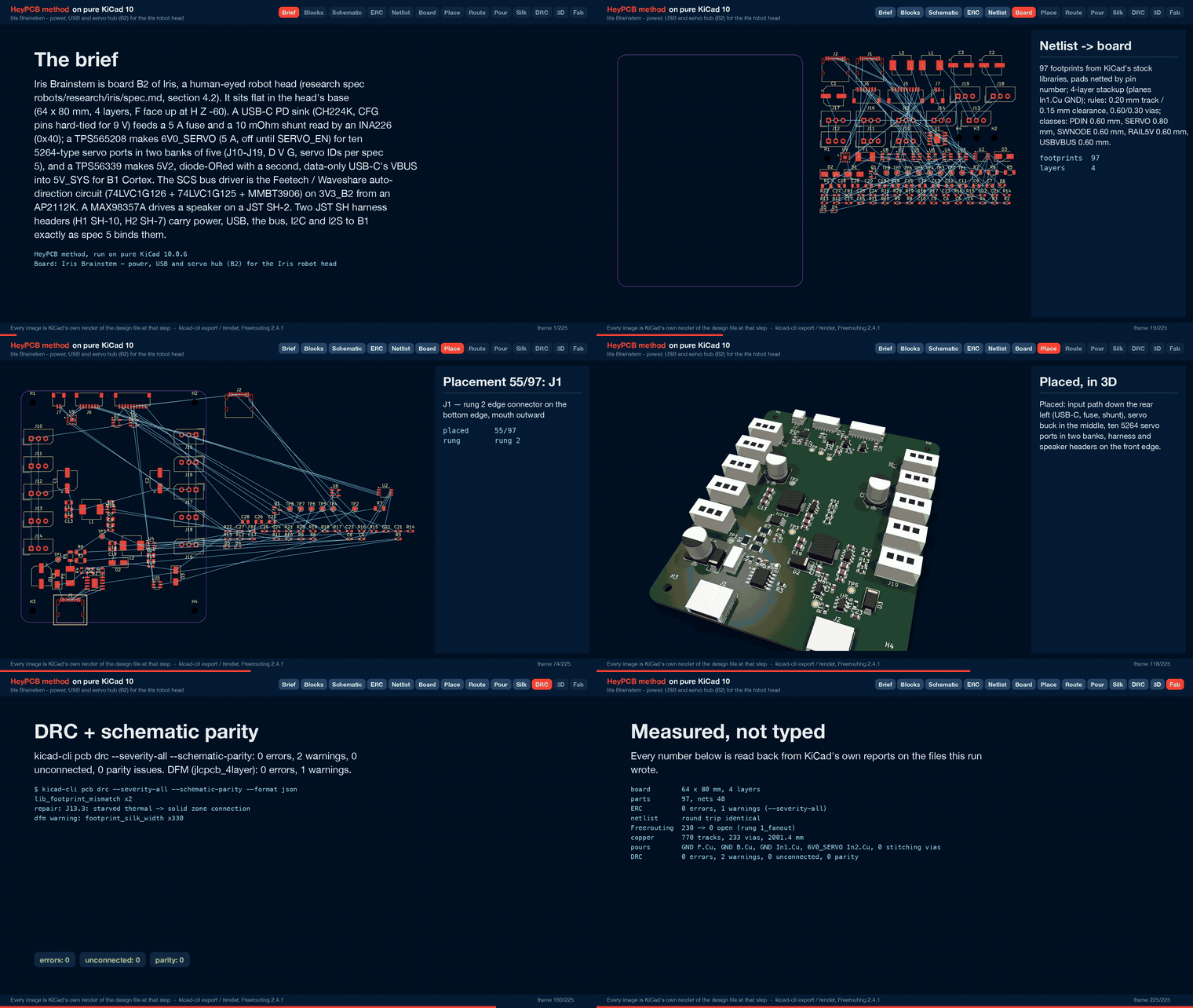
A full run with media on 2026-10-03 (./run.sh --board boards/iris_brainstem, KiCad 10.0.6,
Freerouting 2.4.1). Gate numbers are from report.json. Anything marked read
off the board was measured on kicad/iris_brainstem.kicad_pcb with pcbnew.
Gate
Result
Composition
97 parts, 48 nets (13 block instances of 12 new brainstem_* blocks)
Part binding
85 of 97 parts bound to an LCSC number, 0 unsourced, 0 identity conflicts. The other 12 are not BOM parts: the four mounting holes and the eight test pads. 24 distinct Extended parts, about $72 in JLC loading fees
ERC (kicad-cli sch erc --severity-all)
0 errors, 1 warning (pin_to_pin: the MAX98357A's exposed pad, typed "unspecified" in KiCad's symbol, on GND)
Netlist round trip
identical, 48 nets
Routing, rung 1, fanout on
230 -> 0 open by Freerouting alone, 28.3 s, 53 vias. This solve is kept
Routing, rung 1, fanout off
0 open after the last-mile router closed one 3V3_B2 connection (4 vias), 89.8 s
Net classes
none narrowed (every power class carries a current)
Pours and zones (laid only after a measured 0 open)
Plan: GND on F.Cu, B.Cu and In1, 6V0_SERVO on In2. The 25 board.zones above them, with 180 zone vias (GND 105, VIN 36, VBUS_PD 20, 5V_SYS 11, 6V0_SERVO 8). 0 open after the pours and after stitching, 0 island-repair vias
Silkscreen
55 words and marks placed (24 words, 30 port letters, the speaker's "+"), 39 designators seated and 34 hidden, the 6 back-side title lines placed as one block (offset 5.0, -3.0 mm from the brief's spot). The text displaced 25 GND stitching vias; 6 footprint silk strokes at or past the edge were dropped
fresh, 0 errors, 0 unconnected, 0 parity issues, 2 warnings (lib_footprint_mismatch on J1 and J2: the silk clip dropped 3 of each receptacle's 5 silk strokes at the rear edge, read off the board). One repair before the final check: J13 pin 3's starved thermal became a solid zone connection
DFM (jlcpcb_4layer)
0 errors, 1 warning: 330 stock-footprint silk strokes at 0.12 mm, which the fab prints at its 0.15 mm minimum
Fab gate
ready, no blockers. 4 copper gerbers and a gerber job with LayerNumber 4, 1.6 mm; drill, BOM, JLC CPL (9 rotations corrected), schematic PDF, STEP
3D, renders, video
all ran: 63 3D frames, the renders (492.7 s, on a machine shared with other boards' runs) and the design-process video (225 stills; 151.4 s at 1920 x 1080 by ffprobe)
Nothing on the board was edited by hand: every track came from Freerouting, every pour and stitching
via from the pipeline.
Why the brief looks the way it does
Measured on the runs of 2026-10-03; each reason is also in board.json beside its key.
B.Cu is a power layer. Seven B.Cu track keep-outs keep Freerouting's signals off the bank
strips, the front bar, the VIN band and the 5V_SYS spine, so no signal track splits the zones
there.
Stitched zones carry the higher priority. Where two zones of one net overlap, only the higher
priority fills. vin_col (stitched, F.Cu and B.Cu) placed 0 vias under the B.Cu VIN band until
the band went one priority below it; then 29 (27 after the last placement changes).
In2 keep-outs give the via fields room. A stitch via must clear other nets' tracks on every
layer, so In2 tracks are kept out of the input column and the servo buck's input and output via
fields. The 5V2 buck's In2 keep-out was narrowed to x 40.6-44.6: wider, the USB pair could not
leave the rear right and the USB D- line stayed open.
The test pads sit on their own rails. A row of test pads across the middle needed long traces
through the power copper; the VIN pad's trace cut the servo buck's output-capacitor ground off its
vias (its GND return fell to 0.59 mm).
The 5 V rails stay at 0.6 mm, and 5V2's output has a zone. At 0.8 mm Freerouting ran 5V2 and
5V_SYS as long In2 runs, which rate lower on 0.5 oz copper, and left the USB D- line open. At
0.6 mm 5V2 is F.Cu only, but its routed track from L2 to D2 measured 0.51 mm at the min-cut,
1.5 A at 10 C against the 1.56 A peak. The v5v2_out zone, added on the same route, took it to
1.04 mm (2.5 A).
The 5V_SYS spine's links were moved to clear other nets. Its front link sat behind H1's USB_DP
track (min-cut 0.25 mm) until it moved to x 41.5-45; its rear arm knocked out the 5V2 buck's VIN
field (0 vias) until it moved to y 61.2-63.4.
C3, TP1 and the PD OK row were moved for their labels. C3 moved 2 mm toward the rear so J14's
D / V / G letters fit; TP1 moved to (12.8, 58.3) and the CH224K's support row 0.25 mm lower so
"VIN" and "PD OK" find a spot. The speaker's "+" is a silk.switches entry, because
silk.polarity would also print "-" beside the grounded mounting tabs.
copper_cut.py sums duplicate graph edges in 64 bits. J1's A4 / B9 and A9 / B4 VBUS pads
overlap, and two infinite-capacity edges summed in 32 bits wrapped negative and read as a flow of
0. quack_core's copy has the same line.
Check before ordering
The charger must offer 9 V at 3 A (27 W or more). The CH224K asks for 9 V only. A charger
without a 9 V profile stays at 5 V: the PD OK LED stays off, the TPS565208 cannot make 5.93 V from
5 V (its maximum duty of 83 % needs at least 7.1 V in), and firmware must keep SERVO_EN low (spec 8:
only above 8.5 V VIN). The 5V2 buck runs in dropout at 5 V, so 5V_SYS is lower until 9 V arrives.
Part stock. The TPS565208DDCR (C2650336) had 1,233 in stock at the 2026-10-03 lookup. The
spec's fallback is the TPS54560BDDAR (C1850354, 11,483 then), which needs a 5 A Schottky and a
different package: a re-layout of the servo buck, not a drop-in. Re-check every part's stock at
order time, in particular CH224K C970725 (7,051), SM07B-SRSS-TB C160406 (9,286), FXL0630-5R6-M
C475914 (10,037) and the 54.9 k resistor C23077 (15,112). 24 distinct Extended parts.
Inrush at plug-in. 470 uF (C3) and the bucks' input capacitors sit on VIN behind F1 and R1,
with nothing to limit the inrush when the contract steps VBUS to 9 V. USB-C and USB PD limit the
capacitance a sink may present; a charger may see this as an over-current and drop the contract.
The spec chose this bulk; test with the intended chargers, and add a soft-start switch in a
revision if one trips.
Servo buck stability with 940 uF of electrolytic bulk. TI's table for the TPS565208 (D-CAP2)
gives 20-68 uF of output capacitance at 5-6.5 V out; C1 and C2 add 940 uF of aluminium
electrolytic at the banks. Their ESR damps them, but check load steps and ripple on the bench.
Copper weight. The ratings above assume JLC's standard 4-layer build: 1 oz outer, 0.5 oz inner.
The gerber job the pipeline writes declares 35 um on all four layers; order the stack-up the
ratings assume, or re-rate. 2 oz outer copper would raise the outer-layer share of each figure by
about 65 % (2^0.725).
Connector ratings. The HRO TYPE-C-31-M-12's VBUS current rating and the 5264 headers'
per-pin rating were not checked against data sheets; the spec's per-port stall is 1 A.
B-side clearance. The 5264 headers' tails and the USB-C shell legs protrude below the board;
check them against the base plate (spec: 2 mm on the B side).
JLC's CPL. The pipeline corrected 9 rotations. Check the placement preview, in particular the
polarity of D1-D3, C1-C3 and D6, and pin 1 of U1-U9.
Firmware is not written. The board relies on it (spec 8): SERVO_EN only while the INA226 reads
VIN of 8.5 V or more, cut the servos above a 3.3 A one-second average, stagger servo starts by
2 ms or more, provision servo IDs one at a time (every servo ships as ID 1).
Data sheet facts used
Each value is cited where it is used, in the block files' notes. Data sheets were read for values
and are not stored in this repository.
WCH CH224 data sheet V2.1 (https://www.wch.cn/downloads/file/301.html): CFG1/2/3 = 0/0/0 requests
9 V; CFG1's resistor left open requests 20 V; VDD needs 1 uF and a series resistor from VBUS, the
VBUS pin a series resistor (reference schematic: 1 kOhm, 10 kOhm); VDD is held at 3.24-3.36 V.
TI TPS565208, SLVSE72B (https://www.ti.com/lit/ds/symlink/tps565208.pdf): VFB 0.760 V typical
(0.753-0.767 V); 3.3-4.7 uH and 20-68 uF for 5-6.5 V out; maximum duty 83 %; EN high 1.6 V min.
TI TPS56339, SLVSEI2A (https://www.ti.com/lit/ds/symlink/tps56339.pdf): VREF 0.802 V typical;
5.6 uH and 2 x 22 uF for 5 V; EN has an internal pull-up; BOOT needs about 30 Ohm and 0.1 uF.
TI INA226, SBOS547 (https://www.ti.com/lit/ds/symlink/ina226.pdf): A1 = A0 = GND is 0x40; shunt
full scale 81.92 mV (8.19 A with 10 mOhm); 10 Ohm or less per input filter line.
The Iris Brainstem design files in this folder (board.json, copper.py, copper_cut.py, this
README) and the brainstem_* blocks are released under the CERN Open Hardware Licence Version 2 -
Strongly Reciprocal (CERN-OHL-S-2.0). KiCad's symbol, footprint and 3D libraries keep their own
licence (CC-BY-SA-4.0 with the KiCad library exception). Part numbers and stock figures are
catalogue facts.
Files
board.json: the brief. Blocks, net classes, keep-outs, power zones, placement (with a reason per
lock), routing and silk settings.
copper.py (KiCad's Python) and copper_cut.py (numpy and scipy): the copper measurement above.
They write build/iris_brainstem/copper.json, copper_geom.json and copper_cut.json.
../../blocks/brainstem_*.json: the 12 blocks written for this board. Each block's notes give the
KiCad 10 symbol pinout it was wired from and the data sheet its values came from.
../../parts/lcsc_pinned.json: the 7 parts and 3 resistor values this board added, each with its
2026-10-03 lookup.
The pipeline's outputs are in build/iris_brainstem/ (not committed): report.json, the KiCad
project, fab/ (gerbers, drill, BOM, JLC CPL, schematic PDF, STEP), the renders and the video.
To rebuild, from the repository root:
bash
./run.sh --board boards/iris_brainstem              # the pipeline, with renders and video (5-15 min)
/Applications/KiCad/KiCad.app/Contents/Frameworks/Python.framework/Versions/Current/bin/python3 \
    boards/iris_brainstem/copper.py                 # power copper -> build/iris_brainstem/copper*.json
python boards/iris_brainstem/copper_cut.py          # a Python with numpy and scipy
Brain board for the Open Duck Mini: Pi Zero 2W carrier, 14-servo STS bus, fused 2S power path in stitched copper zones (15-18 A battery side), USB-C charging with balancing, IMU.
It measures 64 × 80 mm and has 4 copper layers, 1.6 mm thick.
What parts does the Iris brainstem use?
97 parts, built around the SN74LVC1G125DBVR-TP, SN74LVC1G126DBVR-TP, CH224K and INA226AIDGSR. The full list of its parts is on this page, with links to each part's symbol and footprint where PCBKit's library has them.
Where can I download the Iris brainstem KiCad files?
From the HeyPCB/iris-brainstem repository on GitHub, at the commit this page was made from: the board is kicad/iris_brainstem.kicad_pcb and its schematic kicad/iris_brainstem.kicad_sch. PCBKit opens the board in the browser, with nothing to install.
Can I use the Iris brainstem design in my own project?
Its repository publishes it under the CERN-OHL-S-2.0 licence: you may reuse it on that licence's terms (keep the author's notice, and for a copyleft licence share your changes alike).