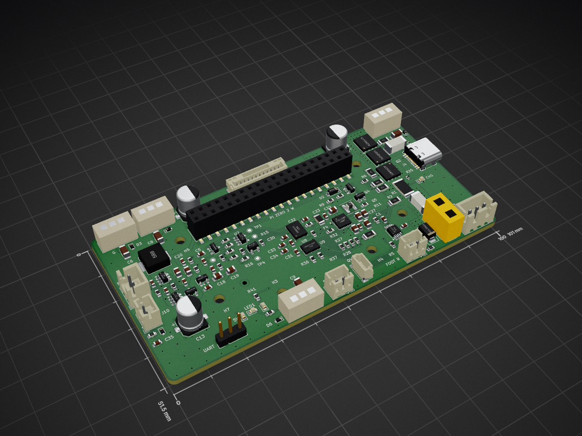
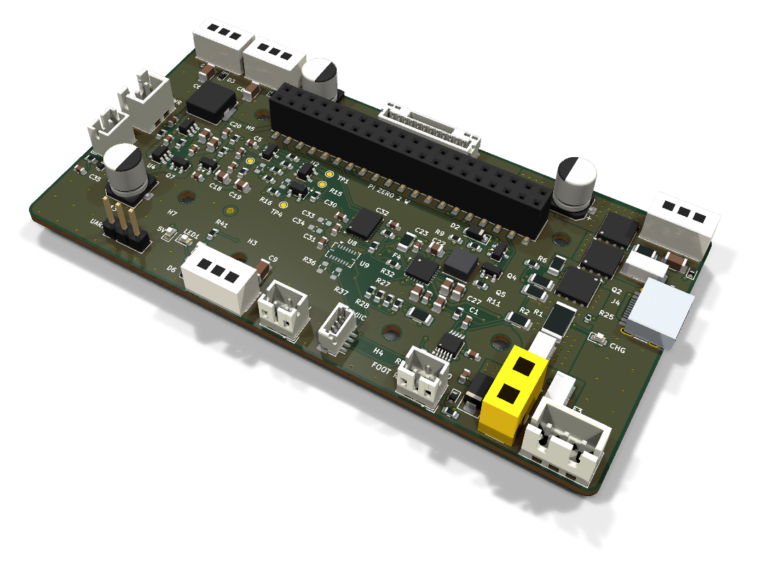
Brain board for the Open Duck Mini: Pi Zero 2W carrier, 14-servo STS bus, fused 2S power path in stitched copper zones (15-18 A battery side), USB-C charging with balancing, IMU. 4-layer KiCad 10 board, fit-checked in the duck's CAD.
Quack core is an open-source printed circuit board by HeyPCB, from the HeyPCB/quack-core repository on GitHub, published under the CERN-OHL-S-2.0 licence. It is a 4-layer board of 101 × 51.5 mm with 138 parts on 117 nets, routed with 1,229 tracks and 224 vias.
It is built around the SN74LVC1G125DBVR-TP, SN74LVC1G126DBVR-TP and INA226AIDGSR, with the TPS56339DDC, BMI088 and BNO055 among its other parts. Its parts include 41 resistors, 36 capacitors, 15 connectors, 12 diodes and 9 ICs. It belongs with the robots and motor control and sensors and measurement boards of this library.
The brain board for the Open Duck Mini: a Pi Zero 2W carrier with the 14-servo STS bus, a fused and switched 2S power path laid in stitched copper zones, USB-C charging with balancing, and the IMU.
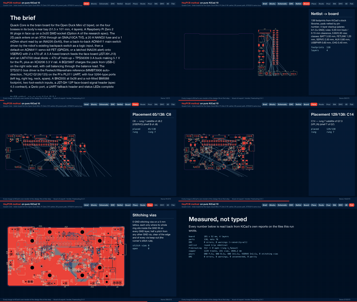
Part of HeyPCB's open robot boards. Designed end to end with the HeyPCB method on
KiCad 10 (headless pipeline, Freerouting 2.4.1); every number below is measured on the files in this repository.
Mentions of ./run.sh, docs/rules/, blocks/ or parts/ refer to the heypcb-kicad SDK that produced them.
Quack Core is a brain board for the Open Duck Mini (v2), the open-source miniature biped by Antoine
Pirrone and contributors. It is a carrier for a Raspberry Pi Zero 2 W and it bolts onto the four
existing trunk_top bosses in the duck's rear bay. It takes the 2S pack through a 20 A fuse, a
1 mOhm shunt and a back-to-back P-FET switch, drives the STS3215 servo bus, and charges and balances
the pack from USB-C. It was designed with the HeyPCB method on KiCad 10 (10.0.6), by heypcb-kicad's
headless pipeline with Freerouting 2.4.1, from the brief in board.json and the research spec
robots/research/duck/spec.md (Option A).
This board has not been fabricated, assembled or powered. Everything below is what KiCad, the
pipeline and the CAD scripts measured on the design files. Nothing here has been tested on
hardware or in the robot, and nothing here contains or tests software.
Specs
Pi Zero 2 W carrier. The Pi plugs in face-up on a 2x20 SMD socket (PM254-2-20-S-8.5,
C3975165), 8.5 mm tall, on four M2.5 standoffs (not supplied) on its 58 x 23 mm hole pattern.
The board's 5.1 V back-powers the Pi through header pins 2 and 4. Do not also plug the Pi's PWR
micro-USB.
Pack input: a vertical XT30 (J2), an SMAJ10CA bidirectional TVS (D1), a 20 A Littelfuse
NANO2 (F1, 0451020.MRL) and a 1 mOhm 3 W 2512 shunt (R1). An INA226 at 0x40 reads the shunt and
the pack voltage; its ALERT goes to GPIO4 and to the servo-kill latch.
Main switch: two AON6411 P-FETs, source to source (Q1, Q2). The robot's existing backpack
slide switch is re-used as a logic switch on J5 and carries about 80 uA. A reversed pack leaves
both FETs off.
Servo power: a third AON6411 (Q3) switches VSYS onto VSERVO. It is on by default: GPIO26 (with
a 100 k pull-down) or a latched INA226 ALERT turns it off. VSERVO has 2 x 470 uF / 16 V bulk
(C10, C11) and 10 uF plus an ESD5Z5.0 on DATA at each port.
Servo bus: an exact copy of the Waveshare Bus Servo Adapter (A) / Feetech reference half-duplex
driver (74LVC1G126 + 74LVC1G125 + MMBT3906) on the Pi's PL011 UART (GPIO14/15), with the
spec's additions: 0 ohm source-select links, a J16 header for an external USB-UART, a DNP RTS
link, a DNP DATA pull-up and four DNP test pads.
Servo ports: four 5264-type 3-pin headers (HC-5264-3A, C2845815), DATA / VSERVO / GND: J6 left
leg, J7 right leg, J8 neck chain, J9 spare.
Pi rail: an LM74700 + AO3400A ideal diode with 470 uF hold-up behind the 5 A face/aux fuse
(F2), then a TPS56339 3 A buck to 5.10 V (53.6 k / 10 k on a 0.802 V reference) and an XC6206
3.3 V LDO for the board's logic.
Charger: BQ25887 2S boost charger from USB-C (J4, HRO TYPE-C-31-M-12, 5.1 k on each CC, a plain
sink) through a 2 A PTC (F4), with cell balancing through the balance lead's mid tap (J3 pin 2).
Input limit 1.48 A (750 ohm on ILIM). It taps the pack ahead of the switch through a 5 A NANO2
(F3), so it charges with the robot switched off. Orange CHG LED, /INT to GPIO16.
IMU: BNO055 at 0x28 (fitted) and a BMI088 footprint at 0x18/0x68 (not fitted).
Face link (the shared contract with the Quack Face board, spec 4.5): J12 JST-GH 12P top entry,
J13 JST-XH 2P with the fused battery rail.
Other I/O: foot switches on J10/J11 (JST-PH 2P, 1 k / 100 nF RC and ESD), a Qwiic port (J14,
JST-SH 4P top entry, 3.3 V), green 5V LED, red LED1/LED2 on GPIO5/GPIO6.
Board: 101 x 51.5 mm (CAD x -93.5 to -42.0, y -50.5 to +50.5), 1.6 mm, 4 copper layers.
F.Cu signal with a GND pour, In1 a GND plane, In2 signal with a VSERVO pour, B.Cu signal with a
GND pour, and the power path laid as stitched copper zones on F.Cu, In2 and B.Cu (see Power
zones). Single-sided assembly. Four non-plated 2.7 mm holes for M2.5 screws on the bosses, and
four more for the Pi's standoffs. The front edge is notched 0.8 mm between CAD y -28.25 and
+28.25 to clear the trunk_top chamfer (see CAD fit).
Option A: the Pi moves into the body
Today the Pi Zero 2 W, its 5 V UBEC and the amplifier sit on the head's ceiling, and a harness
through the 4-DOF neck carries 7.4 V, USB, I2C and the foot-switch wires down to the body (spec
1.4). Quack Core takes the research spec's Option A (spec 2.6): the Pi plugs into this board, in the
body, next to the battery, the servo bus, the IMU and the foot switches. What that changes:
Update the URDF masses before retraining. The Pi (about 10 g) and the UBEC (about 15 g,
replaced here by the on-board buck) leave the head and join the trunk. Both figures are the
spec's estimates. The walk policy was trained on the URDF's mass properties (head_assembly
352.6 g, trunk_assembly 698.5 g), so update both links, add this board's own mass to the trunk,
and retrain (spec 2.6, 7). This board's mass was not measured.
Camera. CSI would have to cross the +/-160 degree head-yaw joint. Either run a round
CSI-to-HDMI extension through the neck (Arducam B0091, with a 22-to-15-pin cable at the Pi), or
leave the camera off. The walk runtime does not use it (spec 2.6).
Runtime: configuration only (spec 3.10). No Python changes:
/boot/firmware/config.txt: enable_uart=1 and dtoverlay=miniuart-bt. The PL011 moves to
GPIO14/15 and Bluetooth stays up for the gamepad. 1 Mbps is 48 MHz / 16 / 3 exactly.
cmdline.txt: remove console=serial0,115200.
A udev rule, KERNEL=="ttyAMA0", SYMLINK+="ttyACM0", so the hard-coded /dev/ttyACM0 in
the runtime still opens the bus (or edit those defaults).
Keep dtparam=i2c_arm=on. If the BNO055 reads glitch, apply Adafruit's i2c_arm_baudrate
fix for its clock stretching.
Keep the I2S amplifier overlay. Every GPIO number the runtime uses is unchanged.
The neck harness becomes J12 (12 signals), J13 (the fused battery rail for the face board's
own 5 V) and the neck servo chain on J8.
Wi-Fi and Bluetooth move inside the PLA body, next to the cells. The spec estimates this as
acceptable but slightly worse.
No first-hand report of an STS3215 bus on a Pi's GPIO UART at 1 Mbps was found (spec 3.10).
J16 and two 0 ohm links are the fallback: remove R17 and R18 and drive the same buffer from a
3.3 V USB-UART on J16 (1 GND, 2 TXD into the board, 3 RXD out of it).
Pinouts
Pi Zero 2 W header (J1)
The 2x20 socket's footprint is the mirror image of the Pi's header (socket pad 2n-1 meets Pi pin
2n), so the block wires each socket pad to the net of the Pi pin it meets. The table is in Pi pin
numbers. Every GPIO number the walk runtime uses is the one it uses today (spec 3.8).
Pi pin
GPIO
Net
Pi pin
GPIO
Net
1
3V3 out
not connected
2
5V
5V (board's 5.10 V in)
3
GPIO2
I2C_SDA
4
5V
5V
5
GPIO3
I2C_SCL
6
GND
GND
7
GPIO4
INA_ALERT
8
GPIO14
UART_TX (servo bus)
9
GND
GND
10
GPIO15
UART_RX (servo bus)
11
GPIO17
UART_RTS (DNP link to TXEN)
12
GPIO18
I2S_BCLK
13
GPIO27
FOOT_R
14
GND
GND
15
GPIO22
FOOT_L
16
GPIO23
EYE_R
17
3V3 out
not connected
18
GPIO24
EYE_L
19, 21, 23
GPIO10, 9, 11
not connected
20
GND
GND
25
GND
GND
22
GPIO25
PROJ
27, 28
GPIO0, 1 (ID EEPROM)
not connected
24, 26
GPIO8, 7
not connected
29
GPIO5
LED1
30
GND
GND
31
GPIO6
LED2
32
GPIO12
ANT_R
33
GPIO13
ANT_L
34
GND
GND
35
GPIO19
I2S_LRCLK
36
GPIO16
CHG_INT
37
GPIO26
SERVO_KILL
38
GPIO20
I2S_DIN
39
GND
GND
40
GPIO21
I2S_DOUT
I2C1 carries the BNO055 (0x28), the INA226 (0x40), the BQ25887 (0x6A or 0x6B, see Check before
ordering), the BMI088 footprint (0x18 / 0x68) and the Qwiic port. The board adds no I2C pull-ups:
the Pi's own pull-ups on GPIO2/3 serve the bus.
Face link: J12 and J13 (the contract with Quack Face)
Both match the Quack Face board (commit 250de3c on robot-quack-face), whose harness runs pin n
to pin n.
J12, JST-GH 12-pin top entry, BM12B-GHS-TBT (C2983891), spec 4.5 unchanged:
Pin
Net
Pin
Net
1
GND
7
GND
2
I2S_BCLK (GPIO18)
8
EYE_L (GPIO24)
3
GND
9
EYE_R (GPIO23)
4
I2S_LRCLK (GPIO19)
10
PROJ (GPIO25)
5
I2S_DOUT to the amplifier (GPIO21)
11
ANT_L (GPIO13)
6
I2S_DIN from the microphone (GPIO20)
12
ANT_R (GPIO12)
The two mounting pads are on GND. The spec named the side-entry SM12B-GHS-TB. The board's front
edge sits 1.9 mm from trunk_top's rear wall, so a side-entry plug facing forward could not be
inserted. The top-entry part has the same housing and pinout.
J13, JST-XH 2-pin (B2B-XH-A, C158012): pin 1 VBAT (VBAT_AUX, the pack after the main switch
and the 5 A fuse F2), pin 2 GND. F2 also feeds the Pi rail. The spec's face worst case (about
2.6 A at the pack) plus the Pi (about 1.4 A) is below 5 A.
Other connectors
Positions are body centres, in the CAD frame of the print STLs (+x forward, +y the robot's left,
mm), read off the final board.
Ref
Function
Part (LCSC)
Pin 1 / 2 / 3
Centre (x, y)
J2
Pack in
AMASS XT30UPB-M vertical (C428721)
- (GND, the chamfered end) / + (VBAT_IN)
(-87.3, -35.0)
J3
Balance lead
JST-XH 3P B3B-XH-A (C144394)
not connected / mid tap / not connected
(-90.0, -44.0)
J4
USB-C charge input
HRO TYPE-C-31-M-12 (C165948)
VBUS, CC1/CC2 5.1 k to GND, no data
(-62.0, -47.2), mouth 0.95 mm past the right edge
J5
Backpack switch (logic)
JST-PH 2P (C131337)
SW_N / GND (closed = on)
(-90.5, +1.0)
J6
Servo bus, left leg
HC-5264-3A (C2845815)
DATA / VSERVO / GND
(-45.3, +43.7)
J7
Servo bus, right leg
HC-5264-3A
DATA / VSERVO / GND
(-45.3, -44.7)
J8
Servo bus, neck chain
HC-5264-3A
DATA / VSERVO / GND
(-45.3, +32.5)
J9
Servo bus, spare
HC-5264-3A
DATA / VSERVO / GND
(-90.4, +12.2)
J10 / J11
Foot switch L / R
JST-PH 2P
switch (GPIO22 / GPIO27 through 1 k) / GND
(-74.0, +47.1) / (-90.5, -22.5)
J14
Qwiic (3.3 V I2C1)
JST-SH 4P top entry BM04B-SRSS-TB (C160390)
GND / 3V3 / SDA / SCL
(-88.9, -7.8)
J16
External UART for the bus
1x3 2.54 mm (C2937625)
GND / TXD in / RXD out
(-89.5, +32.0)
J2's polarity is the footprint's: KiCad's AMASS XT30UPB-M footprint prints - beside pad 1, at the
housing's chamfered end, and + beside pad 2, and the chamfered side of an XT30 is its negative
contact. Pad 2 (+) faces F1; pad 1 (-) is at the rear edge.
J3 uses only the balance lead's mid tap. Its B- pin is the cell side of the pack's BMS: tying it to
the board's ground would bypass the BMS's discharge FETs. So pins 1 and 3 are not connected.
Power path and what the copper carries
text
J2 XT30 ─┬─ D1 SMAJ10CA ─ GND
         ├─ F3 5 A ─ BQ25887 BAT (charger, J4 USB-C, J3 mid tap)
         └─ F1 20 A ─ R1 1 mOhm (INA226 0x40) ─ Q1 ┐ AON6411 back to back, gates on J5
                                                Q2 ┘
                                                 │ VSYS
              ┌──────────────────────────────────┼──────────────────────────┐
         Q3 AON6411 servo kill              F2 5 A ─ VBAT_AUX ─ J13 (face)    R8 / Q4 / Q5 gate drive
         (GPIO26, INA226 ALERT)                      └─ LM74700 + AO3400A ─ 470 uF ─ TPS56339 5.10 V ─ Pi pins 2/4
              │ VSERVO                                                               └─ XC6206 3.3 V
         C10, C11 470 uF; J6, J7, J8, J9 (10 uF + ESD5Z each)
The pack current runs in a straight column down the board's right side: the XT30 at the rear, then
F1, R1, Q1, Q2 and Q3 one above the other, with Q3's drain at the front, beside C10 and J7. The
FETs face source row to source row, so QS and VSYS are three short stubs each.
Net classes (from the brief; a class with a current is never narrowed by the routing ladder):
BATT 3.0 mm (VBAT_IN, VBAT_F, VBAT_SH), FETLINK 1.2 mm (QS, VSYS, limited by the AON6411's 0.5 mm
source leads), SERVO 2.5 mm with 2.2 / 1.2 mm vias (VSERVO), AUX 0.8 mm (VBAT_AUX, VPI_IN, 5V,
BUCK_SW), USBPWR 0.6 mm (VBUS), CHG 0.4 mm (the charger's power nets). The tracks only connect the
path; the current is carried by the zones below.
Power zones
After routing reaches 0 open, the pour stage lays the brief's board.zones: each a named net's
copper over a region on chosen layers, above the plan pours, with every pad joined solid (no
thermal spokes), and, where the zone has a stitch pitch, its own via lattice. Board coordinates
are mm from the outline's top-left corner; every reason is also in board.json.
Zone
Net
Layers
Region
Vias (0.6 / 0.3 mm, 1.2 mm pitch)
vbat_in
VBAT_IN
F.Cu, B.Cu
J2's + pad, F1's input pad, F3 and the TVS (x 79-93, y 35.75-45.25)
13
vbat_f
VBAT_F
F.Cu, B.Cu
F1's output pad to the shunt (x 79.9-90.2, y 27.9-35.6), stepped round the Pi standoff at (79.5, 35.5)
12
vbat_sh
VBAT_SH
F.Cu, B.Cu
the shunt to Q1's drain (x 79.9-90.2, y 18.45-27.75)
9
qs
QS
F.Cu
the 0.7 mm gap between Q1's and Q2's source rows (x 79.9-88.3, y 15.65-18.15)
none: no via fits outside the FETs' courtyards
vsys
VSYS
F.Cu, B.Cu
Q2's drain to Q3's sources, F2 and R8 (x 82.6-94.5, y 8.8-15.45)
7
vservo_q3
VSERVO
F.Cu, In2
Q3's drain to C10, J7's V pin and C7 (x 67.6-97.6, y 0.85-9.7), J7's DATA and GND pins left out
26
vservo_q3_b
VSERVO
B.Cu
Q3's corner on B.Cu, stopping at x 90.6
(shares vservo_q3's)
vservo_band_in2, vservo_band_b
VSERVO
In2; B.Cu
along the front edge to C11, J8 and J6; on B.Cu also under the Pi socket (y to 16.6)
none (a lattice there would perforate In1's GND under the ports)
gnd
GND
F.Cu, B.Cu
the whole board under the zones above
55, at 4 mm
The gnd zone exists to join the XT30's - pad and the ports' GND pins solid. Any GND zone makes
the plan's GND stitcher place nothing (it wants each via's ring inside every GND fill), so the
gnd zone stitches GND itself; the plan's own stitching count reads 0. J7's GND pin sits between
Q3 and J7's V pin, so on any one layer only one of the two nets can pass it: VSERVO reaches J7
on F.Cu and In2, and J7's GND leaves on B.Cu, down the right edge to the XT30.
Measured copper on the current path
copper.py (KiCad's Python) lists every track, via and pour of each power net on the final board
and exports the copper (tracks, pads, plan pours and zones) as polygons. copper_cut.py (the
robots CAD environment, it needs scipy) rasterises that copper on a 0.1 mm grid and finds, for
each link of the path, the narrowest cross-section the link's whole current must pass: a
max-flow / min-cut from the link's source pads to its sink pads, over every layer, with tracks,
zones and via barrels together, in parallel. Outer copper is taken as 35 um, inner as 17.5 um
(JLCPCB's standard 4-layer build), via plating as 25 um. Each cut is rated with
heypcb_kicad.route.ipc2221_amps (IPC-2221, I = k dT^0.44 A^0.725), per layer, summed. Each link
is cut a second time with the copper within 1 mm of its pads counted as the pads ("beyond the
pads"): that rates the board's own copper between the parts, apart from the parts' fixed lands.
Link
From, to
Narrowest cross-section (35 um equivalent)
10 C rise
20 C rise
Beyond the pads, 10 C / 20 C
VBAT_IN
J2 pad 2 to F1.1
8.75 mm: F.Cu 6.73, via barrels 2.02
13.5 A
18.3 A
15.3 A / 20.8 A
VBAT_F
F1.2 to R1.1
8.29 mm of F.Cu, at the fuse's output pad
11.1 A
15.0 A
pads 0.9 mm apart
VBAT_SH
R1.2 to Q1 drain
8.38 mm: F.Cu 7.71, a barrel 0.67
12.3 A
16.7 A
pads 0.9 mm apart
QS
Q1 sources to Q2 sources
3.71 mm of F.Cu: the 0.7 mm gap between the two rows of 0.5 mm source leads
Read off the board (copper_cut.json, copper.json) from the full run with
media. Before the zones, the same measurement gave 4.9-8.0 A at a 10 C rise for every link (the
servo rail crossed one 1.2 mm via; the battery path was 3.0 mm tracks).
What this says about 15 A (the spec's design point: 15 A continuous, 30 A peaks; simulated
walking 13.5-14.4 A, spec 3.9). At a 20 C rise on 1 oz outer copper:
The battery side reaches it: VBAT_IN 18.3 A, VBAT_F 15.0 A, VBAT_SH 16.7 A. VBAT_F and
VBAT_SH end on pads 0.9 mm from the next part's pads (fuse to shunt, shunt to Q1), so their
narrowest section is the copper alongside those pads; the zones already surround them.
The servo rail reaches it in total (24.4 A from Q3 to the four ports, GND return 23.7 A),
and per side as the load divides: the left leg and neck 15.6 A, the right leg 8.2 A (VSERVO)
and 10.3 A (GND), the spare port 6.7 A. The right leg is the narrow one: J7's GND pin sits in
the path, so its VSERVO uses only F.Cu and In2 and its GND only B.Cu and In1. With the walking
load divided over two legs (about 5-7 A each, estimated from spec 3.9), each leg's port has margin; a single
leg near its servos' stall current does not.
The two links between the back-to-back FETs do not: QS 8.4 A and VSYS 9.2 A. They end on
the AON6411's three 0.5 x 0.66 mm source leads per FET. Whatever is poured, the copper that can
touch those leads is about 3.7-4.2 mm wide on F.Cu (the slot to the drain pad is 0.67 mm, and no
via fits inside the package's courtyard). That is a property of the 5 x 6 mm DFN package. These
links are 0.7 mm long, lead to lead; IPC-2221's chart is for long conductors, and a sub-
millimetre bridge between two FET packages sheds its heat into them, so this rating says little
about the real limit. It was not measured. A part whose source is a wide tab (or two FETs in
parallel per side) would raise it.
This board demonstrates about 15 A at a 20 C rise on everything except the 0.7 mm FET-to-FET
bridges (8.4-9.2 A by this rule) and the per-leg ports (8.2-15.6 A). Nothing here is a measured
temperature; measure Q1-Q3, F1, R1 and the XT30 under load before trusting a continuous rating.
The path parts themselves are sized for the design point by the spec (3.9): F1 20 A, FETs of
40 A or more, the 3 W 2512 shunt (0.23 W at 15 A), the XT30. The 5264-type servo headers are
rated 3 A per pin (spec 3.4), which a leg chain can exceed while walking, as on the Waveshare
adapter the duck uses today. 2 oz outer copper would raise the outer-layer share of each figure by about 65 % (2^0.725).
The rest of the power copper, read off the board: VBAT_AUX 0.8 mm (117.9 mm, 4 vias of
0.8 / 0.4 mm, on F.Cu, In2 and B.Cu), 5V 0.8 mm (43.9 mm, F.Cu), VBUS 0.6 mm (45.8 mm, 2 vias, mostly
on In2), VBAT_CHG 0.4 mm (30.6 mm, 2 vias). IPC-2221 at a 10 C rise on 1 oz outer copper:
0.8 mm 2.0 A, 0.6 mm 1.7 A, 0.4 mm 1.2 A; on 0.5 oz inner copper they carry less. The charger's
input is limited to 1.48 A by its ILIM resistor.
Where the board differs from the spec
Spec
On the board
Why
THT 2x20 socket C2977589, or leads clipped to 2 mm
The socket sits over trunk_top's tongue, where the gap under the board is 3.0 mm (spec 2.7)
SMBJ10A-class unidirectional TVS (no LCSC number resolved)
SMAJ10CA, bidirectional, 400 W (C19077530)
Found in a live lookup. Bidirectional, so a reversed pack does not drive it into forward conduction; the back-to-back FETs block the reversed pack
JST-GH SM12B-GHS-TB side entry (not resolved)
BM12B-GHS-TBT top entry (C2983891)
Side entry cannot be plugged at the front edge (see Face link). Same pinout; matches Quack Face
Qwiic SM04B-SRSS-TB side entry
BM04B-SRSS-TB top entry (C160390)
The port is at the rear edge; a side-entry plug there would face the battery lid, 1.5 mm behind the board
BQ25887 VBUS straight from the receptacle
2 A PTC (1206L200/16NR, C22374899) between them
Splits VBUS into the receptacle's 0.6 mm net and the 0.4 mm net that enters the VQFN pin; limits a shorted cable to the source's rating
BMI088 SDO1 / SDO2 to GND
through two 0 ohm links (R36, R37, not fitted with the BMI088)
KiCad's symbol types SDO1/SDO2 as outputs; ERC refuses an output tied to a rail
J15 2x5 expansion header, DNP ID EEPROM, DNP pogo pins to the Pi's USB pads
not on this board
Left out of this revision. GPIO7-11 and GPIO0/1 are not connected
Connector positions (spec 2.7 table, "final placement is up to layout")
J6, J7 and J8 along the front edge, J8 beside J6 rather than at the centre (J12 sits there); J5, J9, J11, J14 and J16 along the rear edge; J10 and J13 on the left edge
Every through-hole lead is behind the tongue's end (x < -90.1) or outside its width (|y| > 26). Cable routing to each opening was not checked
Everything else follows the spec's parts table (spec 6): BNO055, the Waveshare/Feetech bus driver
parts, TPS56339, XC6206, LM74700 + AO3400A, AON6411 x 3, INA226, the 1 mOhm 2512 shunt, NANO2
fuses, BQ25887, HRO USB-C, XT30, HC-5264-3A, JST-XH, JST-PH. Part numbers came from live jlcsearch
lookups on 2026-10-02 and are pinned in parts/lcsc_pinned.json with that date.
What it measured
A full run with media on 2026-10-03 (./run.sh --board boards/quack_core, KiCad 10.0.6,
Freerouting 2.4.1). Gate numbers are from report.json. Anything marked read
off the board was measured on kicad/quack_core.kicad_pcb with KiCad 10.0.6's pcbnew.
Gate
Result
Composition
138 parts, 78 nets, 28 no-connects (20 block instances of 15 distinct blocks, all new quackcore_* blocks)
Part binding
119 of 138 parts bound to an LCSC number, 0 unsourced, 0 identity conflicts. The other 19 are not BOM parts: the eight mounting holes and the not-fitted parts (BMI088 U9 with C33, C34, R36, R37; R19, R20; TP1-TP4). 34 distinct Extended parts, about $102 in JLC loading fees
ERC (kicad-cli sch erc --severity-all)
0 errors, 0 warnings
Netlist round trip
identical, 78 nets
Routing, rung 1, fanout on
312 -> 0 open by Freerouting alone (0 at its pass 11), 363.1 s, 109 vias; the last-mile router had nothing to do. This solve is kept. The zones come after routing, so the route is the same as before them (1229 tracks, 109 vias)
Routing, rung 1, fanout off
19 open, 137.0 s, 110 vias
Net classes
none narrowed (the power classes carry a current and are never narrowed)
Pours and zones (laid only after a measured 0 open)
Plan: GND on F.Cu, B.Cu and In1, VSERVO on In2. The ten board.zones above them (see Power zones), with 122 zone vias: GND 55, VSERVO 26, VBAT_IN 13, VBAT_F 12, VBAT_SH 9, VSYS 7. The plan's GND stitcher placed 0 (see Power zones). 0 open after the pours and after stitching, 0 island-repair vias
Silkscreen
12 words placed (see Check before ordering), 57 designators seated and 68 hidden, 6 back-side title lines placed one by one. The text displaced 7 stitching vias, which leaves 224 vias on the board (read off the board: 213 of 0.6 / 0.3 mm, 6 of 0.8 / 0.4, 3 of 2.2 / 1.2, one each of 1.2 / 0.6 and 1.0 / 0.5). 21 footprint silk strokes at or past the edge were dropped
0 errors, 1 warning: 517 stock-footprint silk strokes at 0.10 mm, which the fab prints at its 0.15 mm minimum
Fab gate
ready, no blockers. 4 copper gerbers and a gerber job with LayerNumber 4, 1.6 mm. The JLC CPL corrected 14 rotations
3D, renders, video
all ran: 63 3D frames, the renders (168.5 s) and the design-process video (273 stills; 180.2 s at 1920 x 1080 by ffprobe)
The 8 DRC warnings: 7 lib_footprint_mismatch (J3, J4, J7, J8, J9, C10, C11: all seven sit
at the board edge, where the silk clip dropped their strokes) and 1 silk_over_copper: the
XT30 footprint's own "+" sits on the edge of F1's pad. The two via_dangling warnings of the
run before the zones (the vias in Q1's and Q2's drain pads) are gone: the zones join them.
Nothing on the board was edited by hand: every track came from Freerouting, every pour and
stitching via from the pipeline.
Why the brief looks the way it does
Measured on the runs of 2026-10-02; each reason is also in board.json beside the key.
The power column is locked part by part. XT30, F1, R1, Q1, Q2 and Q3 sit on one line, each
pad facing the next. Q2 is offset from Q1 by one lead pitch (1.27 mm): aligned, Freerouting ran
Q2's gate line through the 0.67 mm slot between Q1's source leads and drain pad and cut off Q1's
source lead 1. Thin track keep-outs along those slots (q1_source_slot and two more) keep gate
lines out without blocking the source net; a keep-out over the whole slot left 6 open.
FETLINK is 1.2 mm. At 1.4 mm with 0.25 mm clearance the class could not reach Q1's own
0.5 mm source leads.
The charger sits under the Pi with every satellite locked. Beside the USB-C, one of its
analog pins (TS, ILIM, MID, CBSET, REGN) was left open on each of three builds; under the Pi with
the resistors on the placer's shelves, ILIM and MID; with the 2.2 k LED resistor where the placer
put it, under the TS / ILIM / MID pins, MID. Now the four resistors of those pins sit in a fan
below them and the LED resistor right of the capacitors.
J9's pin 1 is at board x 35.77 (its body centre at CAD y +12.2). In the rear-left corner its DATA line was left open
once. At x 34.5 the placer put its 10 uF on the DATA side of the header, where the 2.5 mm VSERVO
class could not reach it between the pins and the edge. 1.27 mm to the right, the placer put the
capacitor beside the boss, and Freerouting routed all 312 connections itself.
The routing was searched in parallel copies. Ten candidate briefs each ran from compose in
their own --build directory, three or four at once. Three reached 0 open: one with router
shorts left in (not eligible), one only after the last-mile router, and this one, which
Freerouting routed alone. The board's own runs then rebuilt it from this brief and routed it the
same way.
The XT30's pads were swapped late. The first revision of quackcore_power_in put the pack +
on pad 1. The silkscreen check showed the footprint's own "-" printed beside that pad: KiCad's
AMASS footprint marks pad 1, at the housing's chamfered end, as the negative contact, which is
the XT30's convention. The block now has GND on pad 1 and VBAT_IN on pad 2, and J2 is turned
180 degrees so the + pad still faces F1. Every number in this README is from the run after the
swap.
The power path is zones, not tracks (added 2026-10-03, once the pipeline had board.zones).
The tracks still route first and every gate is unchanged; the zones then took every link from
4.9-8.0 A to the figures in Power path (10 C rise). What shaped them: one zone per net with
distinct priorities (overlapping zones of one net at one priority are a DRC zones_intersect
error); VBAT_F's zone follows the Pi standoff's keep-out circle, because a square notch there
set its cut at 7.5 mm (14.0 A at 20 C) and the stepped edge at 8.3 mm (15.0 A); VSERVO stops
at x 90.6 on B.Cu so that J7's GND pin keeps B.Cu ground (inside the VSERVO zone its only
ground was In1's thermal spokes, 1.4 A); the GND zone stays off In1 (on In1 it left slivers of
the plane, DRC isolated_copper); and the front band is not stitched, so In1's ground under
J6 and J8 stays whole.
The board's front edge has a 0.8 mm notch, from the CAD fit (see CAD fit).
CAD fit in the duck
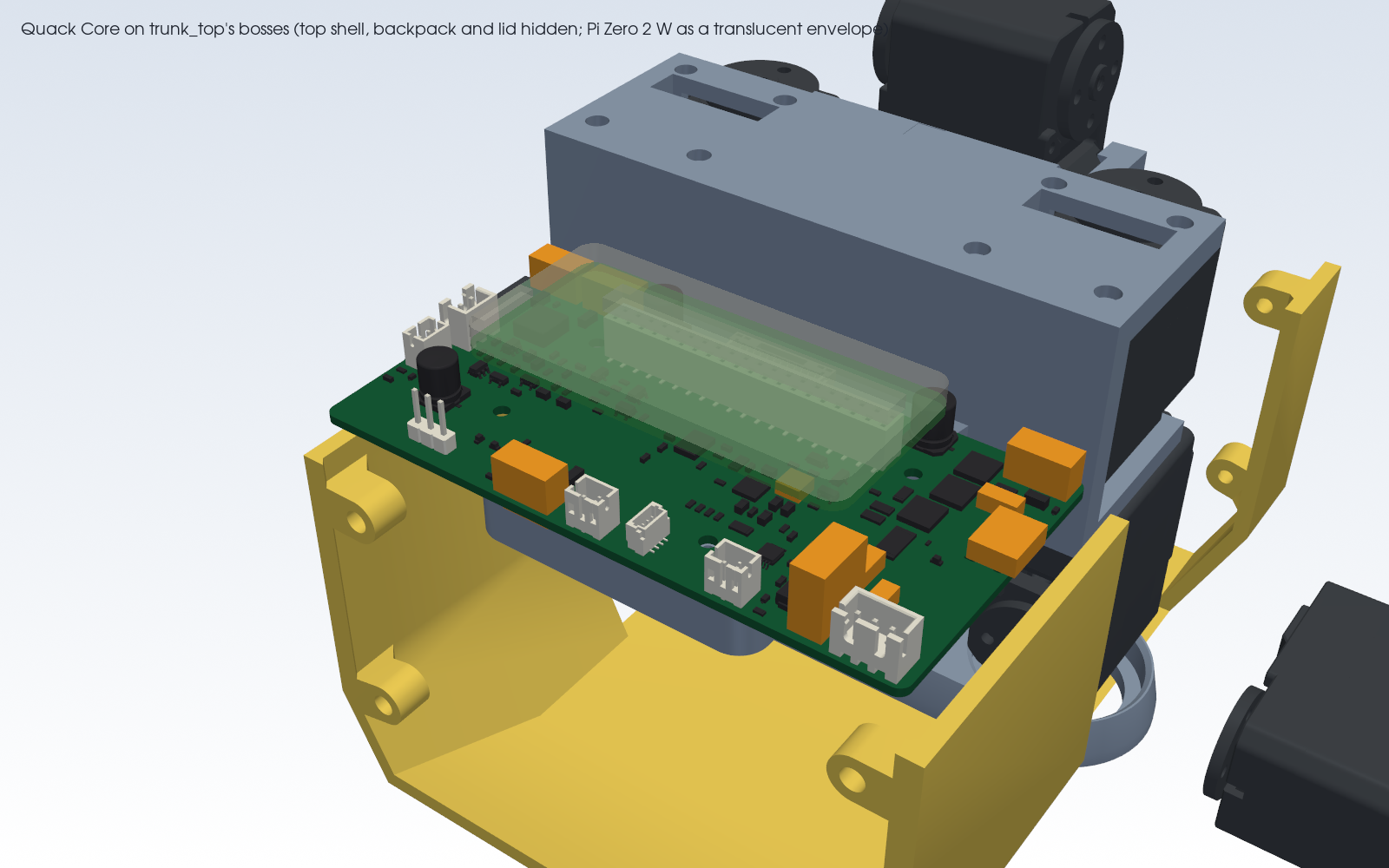
cad/fit.py (the robots CAD environment: CadQuery, trimesh, manifold3d, VTK) places the
pipeline's own STEP (fab/quack_core.step) in the CAD frame of the Open Duck Mini
v2 print STLs, adds an envelope for each part whose KiCad 3D model is missing (named in fit.json,
with its source) and a Pi Zero 2 W envelope on the socket, and measures against every body part:
the print STLs and the URDF's servo cases, horns, cells, holder, BMS and power switch. Clearance
is the smallest distance between points sampled 0.25 mm apart on the assembly and on the body, in
both directions; a sample inside a body counts as interference. The board's bottom face resting on
the four boss tips is the seating, checked separately. Numbers from cad/fit.json:
Check
Result
Holes on the bosses
all four within 0.01 mm of the boss pilots, found by ray casting (pilot 1.99 mm, tips at z -6.10, the board's bottom face)
Interference with any body part
none
Smallest clearance
0.49 mm, board edge to trunk_top's tongue chamfer at the front notch (x -42.8)
body_middle_top (side walls)
0.55 mm, USB-C receptacle mouth to the uncut wall; 2.1 mm to the B2 part with its opening
battery_pack_lid
1.5 mm, board rear edge
body_back
2.16 mm, board corner
Servo cases, horns, cells, holder, BMS, power switch, body_middle_bottom
more than 4 mm
Below the board
through-hole leads 1.8 mm below the bottom face (KiCad's models), against a 3.0 mm gap over the tongue; every lead is behind the tongue's end or outside its width
Free height above each connector (board top to the first body surface)
J2 40.5, J3 18.2, J4 29.0, J5 44.5, J6 35.6, J7 29.6, J8 44.5, J9 44.5, J10 29.2, J11 44.5, J13 29.7, J14 44.5, J16 39.3 mm; above J12 and the Pi socket no body surface (the roof opening)
Pi Zero 2 W envelope
x -81.0 to -51.0, y -32.5 to +32.5, its PCB 11.0 mm above the board top (8.5 mm socket + 2.5 mm header spacer), 3.45 mm of parts on it (estimated): no interference
The front notch. The spec's rectangle put the board's front edge 0.11 mm into trunk_top's
chamfer where the tongue meets the front wall (the edge sat at z -6.10 where the chamfer reaches
-5.99, measured on trunk_top.stl). The outline is set back 0.8 mm along the front edge for
|y| <= 28.25, which gives the 0.49 mm above.
B2, the USB-C opening (spec 5). fit.py cuts a 13.0 x 7.5 mm opening with 1.5 mm corner radii
through the right-hand (-y) side wall of body_middle_top, centred on the receptacle at
x -62.0, z -2.87 (spec: x -62.0, z -2.9), through y -51 to -56 (the wall is y -52 to -55). The
receptacle's mouth is at y -51.45, 3.55 mm inside the wall's outer face. 286.6 mm3 removed; the
result is watertight. It is cad/body_middle_top_usbc.stl (and a faceted STEP in
cad/), Apache-2.0 with the change notice in cad/NOTICE.
Preview renders (headless VTK), written by fit.py to cad/: fit_iso.png (the
board on the bosses, top shell hidden, the Pi as a translucent envelope), fit_top.png (front up,
the Pi hidden, envelopes in orange), fit_section.png (a section at y -14 through two bosses, seen
from the robot's right) and fit_usbc.png (the B2 opening with the receptacle behind it).
Envelopes, not vendor models: the XT30 (11 mm tall, estimated, no drawing read), the four
5264 headers (10 x 4.9 x 6 mm, LCSC row), the NANO2 fuses, the XFL4020 inductor and the USB-C
shell (8.94 x 7.35 x 3.26 mm).
Check before ordering
The board passes ERC, the netlist round trip, DRC with schematic parity, DFM and the fab gate in
KiCad. It has not been fabricated, assembled or powered.
Current. At a 20 C rise on 1 oz outer copper the battery side (15.0-18.3 A) and the servo
rail in total (24.4 A, GND 23.7 A) reach the 15 A design point; the 0.7 mm bridges between the
FETs' source leads (QS 8.4 A, VSYS 9.2 A) and the right-leg port (8.2 A) do not, by IPC-2221.
See Power path. Before a walking test at full current, measure the temperature of Q1-Q3, F1,
R1 and the XT30 under load; 2 oz outer copper is the cheap margin.
Pack BMS. The duck's 8 A / 10 A BMS is the first limit: the spec asks for a 2S BMS rated
20 A continuous or more, 40 A peak or more and 10 mOhm or less (spec 3.1). The XT30 is the
pack connector, and the 2 x 470 uF bulk behind Q3 charges through the BMS each time the servos
are switched on (Q3 turns on in tens of microseconds). Check the BMS's short-circuit trip
against that inrush.
8.4 V on 7.4 V servos. VSERVO is the pack voltage, up to 8.4 V on a full 2S pack. The STS3215
is rated 4-7.4 V with an 8.0 V register limit (spec 1.3; whether shipped servos alarm at 8.0 V is
an open item, spec 8). The BQ25887 charges to 8.4 V by default (REG00 resets to 4.20 V per
cell). It runs with no host, with the robot switched off; to charge to 8.0 V, the Pi must write
4.00 V per cell to REG00 and disable the watchdog (REG05 WATCHDOG = 00) while it runs. Those
settings then hold until the pack is unplugged.
BNO055 axes. The chip is turned so that pin 1 is at its rear-left corner. By the data sheet's
placement figure that turns chip +X toward the robot's left and chip +Y toward its rear, which is
what raw_imu.py's remap needs for imu_upside_down = false (spec 3.6). This was read off a
figure, not tested: check it against the figure (and on the bench, by tilting) before trusting
the walk policy on this board.
BQ25887 I2C address. TI's data sheet gives 0x6A in one place and 0x6B in another (SLUSD89B
8.3.11 and 8.3.11.5). Scan the bus once before writing driver code.
Via in pad.route.via_in_pad_mm put a via in every SMD pad 2.6 mm or wider: Q1, Q2 and Q3's
drain pads (1.2 / 0.6, 1.0 / 0.5 and 2.2 / 1.2 mm) and the charger's exposed pad (0.6 / 0.3 mm).
All four now join a zone on B.Cu. Open holes in a FET pad wick solder: order these vias filled
and capped. The 122 zone vias sit outside every part's courtyard and need nothing special.
Envelopes. The XT30's 11 mm height is an estimate (no drawing was read), and five other parts
are envelopes from catalogue sizes (see CAD fit). The tightest measured gaps are 0.49 mm at the
front notch and 0.55 mm at the USB-C mouth before the B2 cut.
Balance lead. Only the mid tap (J3 pin 2) is used. Check that the pack's balance plug puts
the mid tap on pin 2 (the usual B-, mid, B+ order) and that it mates with a JST-XH header.
No thermistor. TS is a fixed divider at 55.4 % of REGN, between the data sheet's 10 C and
45 C thresholds, so the charger always sees a normal temperature and never sees the pack's.
Pi rail. The board back-powers the Pi through pins 2 and 4 at 5.10 V nominal. Never plug the
Pi's PWR micro-USB at the same time. The Pi sits 11 mm above the board on a socket of 8.5 mm plus
a 2.5 mm header spacer, on four 11 mm M2.5 standoffs (not on the BOM).
Inner copper. The gerber job says 0.035 mm on every layer; that is KiCad's default
stackup, not a fab quote. The copper ratings above assume JLCPCB's standard 0.5 oz inner layers.
Part numbers and stock. The rows this board added were read live from jlcsearch on
2026-10-02. On that date the BQ25887RGER had 987 in stock. Stock and Basic / Extended class go
stale: re-check before ordering. The BOM has 34 distinct Extended parts (about $102 in JLC
loading fees).
Silkscreen.Read off the board: the front carries PI ZERO 2 W, FACE PWR, UART, SWITCH,
QWIIC, FOOT R, 5V, LED1 and CHG, and the D / V letters beside J9 (and G beside J6). The
other words (BATT, L LEG, R LEG, NECK, SPARE, FACE, BALANCE, USB-C CHARGE, FOOT L, LED2 and
20A, which the run before the zones placed and this one did not) found no free spot among the parts and are not printed. The XT30 carries its footprint's
own "+" beside the + pad, toward F1; its "-" falls past the rear edge and is clipped. The back
carries the title and a legend: "servo ports 1 D 2 V 3 G: J6 L LEG J7 R LEG J8 NECK J9 SPARE"
and "J2 XT30 1 - 2 + J13 FACE PWR 1 + 2 - J3 BAL 2 MID". Check the XT30 plug's wiring against
that legend before the first connection.
Licence and attribution
The board files here (board.json, the quackcore_* blocks, the scripts) are part of the
heypcb-kicad repository.
Open Duck Mini (CAD, STLs, URDF, documentation), by Antoine Pirrone (apirrone) and
contributors, is Apache License 2.0 (github.com/apirrone/Open_Duck_Mini; Onshape document
64074dfcfa379b37d8a47762). cad/body_middle_top_usbc.stl is derived from its
print/body_middle_top.stl; the change is stated in cad/NOTICE, and the licence is copied as
cad/LICENSE_Open_Duck_Mini_Apache-2.0.txt. fit.py reads the other print STLs and URDF meshes
from a local copy and does not redistribute them.
Quack Core is a board for the Open Duck Mini. Apache-2.0 grants no trademark rights; no
Disney or BD-X mark is used on the board or in these files.
The Open Duck Mini runtime has no licence file, so none of its code is copied here. Pin and port
assignments are used as interface facts.
Data sheets were read for values and are not redistributed.
Files
board.json: the brief. Blocks, net classes, keep-outs, placement (with a reason per lock),
routing and silk settings.
copper.py (KiCad's Python) and copper_cut.py (scipy): the copper measurement above. They
write copper.json, copper_geom.json and copper_cut.json.
cad/fit.py: the CAD fit, B2 and the previews; writes cad/.
cad/body_middle_top_usbc.stl, cad/NOTICE, cad/LICENSE_Open_Duck_Mini_Apache-2.0.txt: the
B2 part and its attribution.
../../blocks/quackcore_*.json: the 15 blocks written for this board. Each block's notes give
the KiCad 10 symbol pinout it was wired from and the data sheet its values came from.
The pipeline's outputs are in build/quack_core/ (not committed): report.json, the KiCad
project, fab/ (gerbers, drill, BOM, JLC CPL, schematic PDF, STEP) and the media.
To rebuild, from the repository root:
bash
./run.sh --board boards/quack_core                     # the pipeline, with renders and video
/Applications/KiCad/KiCad.app/Contents/Frameworks/Python.framework/Versions/Current/bin/python3 \
    boards/quack_core/copper.py                        # power copper -> build/quack_core/copper*.json
python boards/quack_core/copper_cut.py          # a Python with numpy and scipy
DUCK_CAD=<duck folder> python cad/source/fit.py   # CadQuery + trimesh; needs the Open_Duck_Mini STLs
Iris Brainstem: power and servo hub of the Iris robot head. 9 V USB-C PD in, 6 V / 5 A servo rail in stitched copper zones (measured), 5 V rail, half-duplex servo bus with ten ports, speaker amp.
Face board for the Open Duck Mini's head: eye LEDs, projector driver, I2S amp and mic, antenna servos, shaped to the head. 4-layer KiCad 10 board plus printed standoffs, fit-checked in the head CAD.
Editable KiCad projects for the brain, light, power, and pump boards.
64 parts
Questions
How big is the Quack core PCB?
It measures 101 × 51.5 mm and has 4 copper layers, 1.6 mm thick.
What parts does the Quack core use?
138 parts, built around the SN74LVC1G125DBVR-TP, SN74LVC1G126DBVR-TP, INA226AIDGSR and TPS56339DDC. The full list of its parts is on this page, with links to each part's symbol and footprint where PCBKit's library has them.
Where can I download the Quack core KiCad files?
From the HeyPCB/quack-core repository on GitHub, at the commit this page was made from: the board is kicad/quack_core.kicad_pcb and its schematic kicad/quack_core.kicad_sch. PCBKit opens the board in the browser, with nothing to install.
Can I use the Quack core design in my own project?
Its repository publishes it under the CERN-OHL-S-2.0 licence: you may reuse it on that licence's terms (keep the author's notice, and for a copyleft licence share your changes alike).