2 layers53.3 × 57.6 mm

 kelu124/rp5693
RP569 - PIOs to usb3 ( rp2350 x ch569 )
Rp569 is an open-source printed circuit board by kelu124, from the kelu124/rp569 repository on GitHub. It is a 4-layer board of 50 × 70 mm with 146 parts on 147 nets.
It is built around the CH569W, RP2350B and TLV62569DBVR-TP, with the W25Q128JVSIQ, DM3AT-SF-PEJM5 and TPD2EUSB30DRTR among its other parts. Its parts include 51 capacitors, 51 resistors, 12 ICs, 11 connectors and 7 switches. It belongs with the RP2350 boards of this library.


An open hardware board (KiCad) that pairs a Raspberry Pi RP2350B with a WCH CH569W. The RP2350B generates high-speed data and the CH569 streams it to a host over USB 3.0.
Status: v1.0 (tag v1.0). Schematic complete, PCB fully routed (4-layer, 50×70 mm, rounded corners,
parts on both sides; 0 unconnected, 0 DRC errors) and JLCPCB production files generated. Before ordering:
USB pairs as coupled pairs, silkscreen cleanup, impedance check (see docs/layout.md).
First firmware for both chips in firmware/ (builds, not run on hardware yet).
Schematic PDF. Documentation site: https://kelu124.github.io/rp569/ (GitHub Pages from docs/).
| File | Use |
|---|---|
hardware/jlcpcb/rp569-gerbers.zip | PCB order (gerbers + drill) |
hardware/jlcpcb/rp569-bom.csv | Assembly BOM with LCSC part numbers |
hardware/jlcpcb/rp569-cpl.csv | Assembly placement (CPL) |
Board to fabricate: hardware/rp569-routed.kicad_pcb. Regenerate the files
with python3 hardware/gen/gen_fab.py. Two parts are not stocked by JLCPCB and must be consigned: CH569W and the
Amphenol GSB343K33HR USB3 connector (docs/bom.md).
| Top | Bottom |
|---|---|
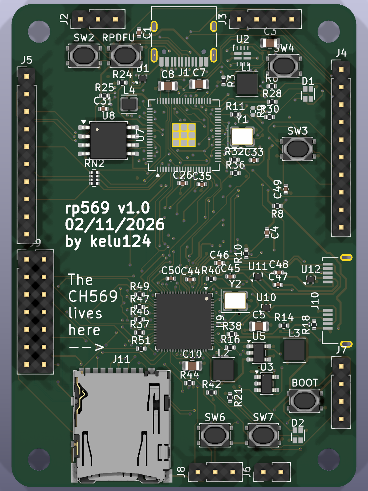 | 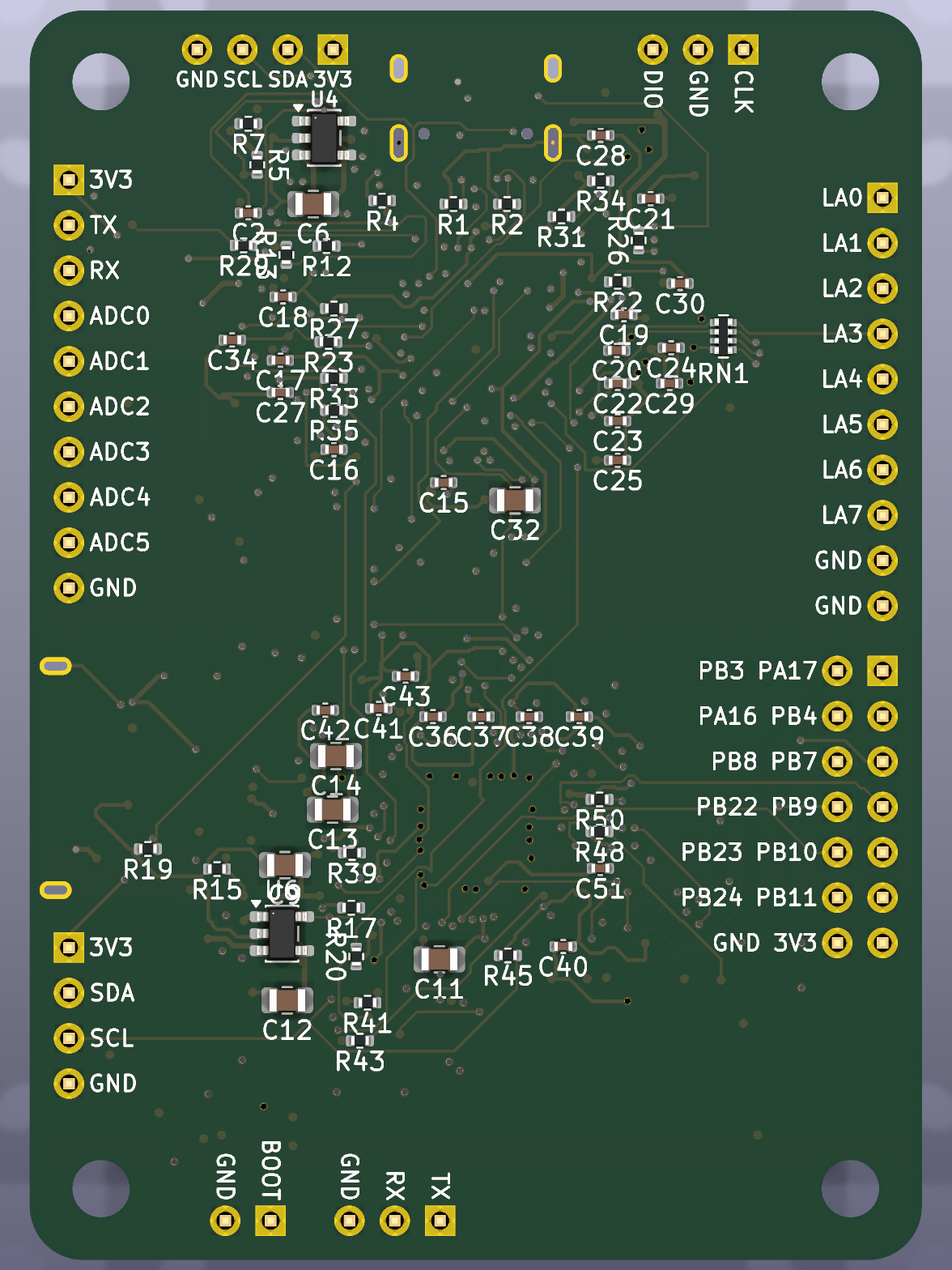 |
| Block | RP2350B | CH569W |
|---|---|---|
| USB | USB 2.0 on USB-C (firmware, debug, test control) | USB 3.0 SuperSpeed, Micro-B connector |
| Storage | QSPI flash | SD card on the eMMC/SD controller |
| User I/O | RGB LED, 2 user buttons | RGB LED, 2 user buttons |
| Boot | BOOTSEL + RUN buttons | BOOT button + jumper (force the USB bootloader on a blank chip) |
| Breakout | I2C header for extra devices | I2C header (bit-banged GPIO) |
Logic analyser: 8 input pins on the RP2350B are sampled by PIO and streamed over the parallel bus to the CH569, then to the host over USB 3.
Power: the RP2350B runs from either USB connector through a TI TPS2121 power mux, so neither back-feeds the other. The CH569 is powered from its own USB3 VBUS through a load switch that the RP2350B controls, so it can be power-cycled and forced into its bootloader during automated tests.
Links between the two chips
specification.md D-003): RP2350B PIO sends, CH569 HSPI receives.| Path | Content |
|---|---|
hardware/ | KiCad project, generated from hardware/gen/board.py (run hardware/gen/build.sh); rp569-routed.kicad_pcb = routed v1.0 board |
hardware/jlcpcb/ | JLCPCB production files: gerbers zip, BOM, CPL |
python/ | Host library: finds the RP2350/CH569 ports by VID/PID/product/UID, one method per firmware command (python/README.md) |
firmware/ | rp2350/ USB command line (LED, dfu, CH569 power/boot/link), ch569/ USB3 serial + SD drive with RP2350 link echo; see firmware/README.md |
datasheet/ | Datasheets as PDF and Markdown (see datasheet/README.md) |
docs/ | GitHub Pages site root (index.md, _config.yml): architecture.md, production.md, pinmap.md (RP2350B ↔ CH569 pin map), power.md, layout.md, bom.md (JLCPCB BOM), ch569-hardware-notes.md, hadposts/ (Hackaday log drafts) |
project/ | Reference projects: HydraUSB3, phantomdrive (see project/README.md) |
specification.md | Requirements (R-xx) and design decisions (D-xxx) |
CLAUDE.md, .claude/ | Project context, todo/done logs, commit log |
| Qty | Value | Footprint | References |
|---|---|---|---|
| 27 | 100nF | Capacitor_SMD:C_0402_1005Metric | C15, C16, C17, C18, C19, C20, C21, C22, C23, C24, C25, C26, C27, C28, C35, C36 +11 |
| 10 | 100k | Resistor_SMD:R_0402_1005Metric | R7, R10, R13, R15, R16, R17, R18, R20, R21, R51 |
| 7 | 10k | Resistor_SMD:R_0402_1005Metric | R11, R27, R33, R34, R37, R39, R40 |
| 6 | 10uF | Capacitor_SMD:C_0805_2012Metric | C3, C5, C6, C9, C12, C32 |
| 6 | 22uF | Capacitor_SMD:C_0805_2012Metric | C7, C8, C10, C11, C13, C14 |
| 6 | 4.7k | Resistor_SMD:R_0402_1005Metric | R31, R32, R35, R36, R44, R45 |
| 6 | 4.7uF | Capacitor_SMD:C_0402_1005Metric | C1, C29, C30, C31, C49, C51 |
| 6 | 47k | Resistor_SMD:R_0402_1005Metric | R19, R46, R47, R48, R49, R50 |
| 4 | 100R | Resistor_SMD:R_0402_1005Metric | R29, R30, R42, R43 |
| 4 | 15pF | Capacitor_SMD:C_0402_1005Metric | C33, C34, C45, C46 |
| 4 | M3 | MountingHole:MountingHole_3.2mm_M3 | H1, H2, H3, H4 |
| 4 | TPD2EUSB30 | Package_TO_SOT_SMD:Texas_DRT-3 | U1, U10, U11, U12 |
| 3 | 1k | Resistor_SMD:R_0402_1005Metric | R23, R26, R38 |
| 3 | 2.2uH | Inductor_SMD:L_Changjiang_FTC303015D | L1, L2, L3 |
| 3 | TLV62569 | Package_TO_SOT_SMD:SOT-23-5 | U4, U5, U6 |
| 2 | 0R | Resistor_SMD:R_0402_1005Metric | R8, R9 |
| 2 | 100R | Resistor_SMD:R_Array_Convex_4x0402 | RN1, RN2 |
| 2 | 23.7k | Resistor_SMD:R_0402_1005Metric | R3, R5 |
| 2 | 27R | Resistor_SMD:R_0402_1005Metric | R24, R25 |
| 2 | 330R | Resistor_SMD:R_0402_1005Metric | R28, R41 |
| 2 | 4.99k | Resistor_SMD:R_0402_1005Metric | R4, R6 |
| 2 | 453k | Resistor_SMD:R_0402_1005Metric | R12, R14 |
| 2 | 5.1k | Resistor_SMD:R_0402_1005Metric | R1, R2 |
| 2 | RGB | LED_SMD:LED_LiteOn_LTST-C19HE1WT | D1, D2 |
| 1 | 10nF | Capacitor_SMD:C_0402_1005Metric | C2 |
| 1 | 12MHz | Crystal:Crystal_SMD_3225-4Pin_3.2x2.5mm | Y1 |
| 1 | 1uF | Capacitor_SMD:C_0402_1005Metric | C4 |
| 1 | 3.3uH | Inductor_SMD:L_Cenker_CKCS201610 | L4 |
| 1 | 30MHz | Crystal:Crystal_SMD_3225-4Pin_3.2x2.5mm | Y2 |
| 1 | 33R | Resistor_SMD:R_0402_1005Metric | R22 |
| 1 | AP2171W | Package_TO_SOT_SMD:SOT-23-5 | U3 |
| 1 | BOOTSEL | Button_Switch_SMD:SW_SPST_PTS810 | SW1 |
| 1 | CH BOOT JP | Connector_PinHeader_2.54mm:PinHeader_1x02_P2.54mm_Vertical | J6 |
| 1 | CH BTN1 | Button_Switch_SMD:SW_SPST_PTS810 | SW6 |
| 1 | CH BTN2 | Button_Switch_SMD:SW_SPST_PTS810 | SW7 |
| 1 | CH EXT | Connector_PinHeader_2.54mm:PinHeader_2x07_P2.54mm_Vertical | J9 |
| 1 | CH I2C | Connector_PinHeader_2.54mm:PinHeader_1x04_P2.54mm_Vertical | J7 |
| 1 | CH UART | Connector_PinHeader_2.54mm:PinHeader_1x03_P2.54mm_Vertical | J8 |
| 1 | CH569 BOOT | Button_Switch_SMD:SW_SPST_PTS810 | SW5 |
| 1 | CH569W | Package_DFN_QFN:QFN-68-1EP_8x8mm_P0.4mm_EP5.2x5.2mm | U9 |
| 1 | LA IN | Connector_PinHeader_2.54mm:PinHeader_1x10_P2.54mm_Vertical | J5 |
| 1 | RP BTN1 | Button_Switch_SMD:SW_SPST_PTS810 | SW3 |
| 1 | RP BTN2 | Button_Switch_SMD:SW_SPST_PTS810 | SW4 |
| 1 | RP EXT | Connector_PinHeader_2.54mm:PinHeader_1x10_P2.54mm_Vertical | J4 |
| 1 | RP I2C | Connector_PinHeader_2.54mm:PinHeader_1x04_P2.54mm_Vertical | J3 |
| 1 | RP2350B | Package_DFN_QFN:QFN-80-1EP_10x10mm_P0.4mm_EP3.4x3.4mm | U7 |
| 1 | RUN | Button_Switch_SMD:SW_SPST_PTS810 | SW2 |
| 1 | SWD | Connector_PinHeader_2.54mm:PinHeader_1x03_P2.54mm_Vertical | J2 |
| 1 | TPS2121 | rp569:TI_RUX0012A_VQFN-HR-12_2x2.5mm | U2 |
| 1 | USB-C (RP2350) | Connector_USB:USB_C_Receptacle_HRO_TYPE-C-31-M-12 | J1 |
| 1 | USB3 Micro-B (CH569) | rp569:USB3_Micro-B_Amphenol_GSB343K33HR | J10 |
| 1 | W25Q128JVS | Package_SO:SOIC-8_5.3x5.3mm_P1.27mm | U8 |
| 1 | microSD | Connector_Card:microSD_HC_Hirose_DM3AT-SF-PEJM5 | J11 |

ackom-a-o/stm32f446-development-board
Custom STM32F446ZET6 development board in KiCad. Prototype hardware, design review and validation log; hardware testing pending.


kartben/hw-testing-rack
3D-printed, tilted test shelf for 16 dev boards: sliding drawers, per-bay ESP32-S3 running Zephyr (USB/IP, power switching, metering), KiCad PCBs, OpenSCAD parts, BOM and an interactive 3D viewer

tombueng/hilprobe
HILprobe: multi-function UUT probe for hardware-in-the-loop testing - RS-485, CAN FD, logic analyzer, 4-ch scope, two programmable UUT supplies. KiCad 10, 6 layers, RP2350B + ESP32-S3.

earlynerd/ELRS-haptics
Battery-powered attitude feedback for FPV flying, with eight haptic actuators around each wrist. An ESP32-C6 receives telemetry over ESP-NOW and controls eight M2003FC1AE/DRV2625 pods using the music robot's UART ring…
o7-machinehum/phantomdrive
Seemingly normal USB drive with a hidden security feature

swittlich/prjfreeman
Open-source flow (yosys + nextpnr) and bitstream documentation for the XC2064, the first FPGA
It measures 50 × 70 mm and has 4 copper layers, 1.6 mm thick.
146 parts, built around the CH569W, RP2350B, TLV62569DBVR-TP and W25Q128JVSIQ. The full list of its parts is on this page, with links to each part's symbol and footprint where PCBKit's library has them.
From the kelu124/rp569 repository on GitHub, at the commit this page was made from: the board is hardware/rp569.kicad_pcb and its schematic hardware/rp569.kicad_sch. PCBKit opens the board in the browser, with nothing to install.
Its repository states no licence, so its author keeps all rights: ask kelu124 before reusing the design.