Skip to the content
PCBKitNew board
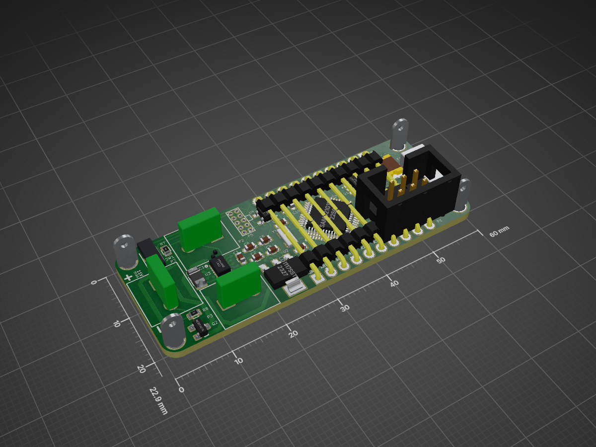
2 layers60 × 22.9 mmElectronutLabs ZeroDriver autosave zeroDriver, the printed circuit board in 3D

ElectronutLabs ZeroDriver autosave zeroDriver

PCBench/PCBench21

resolution = [0.5, 0.5] pcbfolder = '../PCBs/' pcbnames = ["1Bitsy1bitsy"] iters = 30 env = PCBRoutingEnv(resolution=resolution, pcbfolder=pcbfolder, pcbnames=pcbnames) obs, info = env.reset() for in range(iters): act =…

Size
60 × 22.9 mm
Copper layers
2
Thickness
1.6 mm
Parts
53
Nets
63
Pads
204
Tracks, vias
891, 60
Routed
Yes
KiCad
KiCad 5 (file 20171130)
Created
28 Mar 2023
Updated
18 Jan 2024

Overview

ElectronutLabs ZeroDriver autosave zeroDriver is an open-source printed circuit board by PCBench, from the PCBench/PCBench repository on GitHub, published under the MIT licence. It is a 2-layer board of 60 × 22.9 mm with 53 parts on 63 nets, routed with 891 tracks and 60 vias.

It is built around the 74AHC1G125GW, DRV8835DSS and AP2112K-3.3, with the DMG2307L and NCE3407A among its other parts. Its parts include 12 capacitors, 8 resistors, 8 connectors, 5 ICs and 2 diodes. It belongs with the SAM D and SAM boards of this library.

Main components

5

README

README.md

PCBench: A Dataset for Printed Circuit Board Routing

PCBench is a dataset for PCB routing task, it includes a dataset consisting of 164 printed circuit boards (PCB), a data augmentation script to expand the dataset for supervised learning (SL) tasks, and a reinforcement learning (RL) environment.

Dataset

Folder Structure

All the PCB designs in our dataset are stored in the folder PCBs, where each PCB design is stored in a subfolder named {author/org}_{PCB_name}_{design_version(optional)}. Below is the folder structure of the dataset.

text
├── PCBs
│   ├── master_metadata.json
│   ├── subfolder1
│   │   ├── raw.kicad_pcb
│   │   ├── processed.kicad_pcb
│   │   ├── final.json
│   │   ├── metadata.json
│   │   ├── visual.png
│   ├── subfolder2
│   │   ├── raw.kicad_pcb
│   │   ├── processed.kicad_pcb
│   │   ├── final.json
│   │   ├── metadata.json
│   │   ├── visual.png
│   ├── ...

The raw.kicad_pcb is the raw PCB design file, process.kicad_pcb is the file after cleaning up, final.json stores only routing-related information used for ML tasks. metadata.json stores the meta information for each single PCB design. visual.png is a visualization of each single PCB design. master_meta.json contains metadata of all PCBs and global-level information.

PCB Routing Description Language (PCB-RDL)

We propose a JSON specification (final.json for each PCB design) called the PCB Routing Description Language (PCB-RDL) that expresses a PCB routing problem and its solutions intuitively using basic concepts in order to facilitate research into automated PCB routing using ML. Following figure shows is an example of PCB with marked components in PCB-RDL (Left) and it corrsponding PCB-RDL (Right).

PCB example

Data Augmentation

Run

The augmentation data can be generated with the script Scripts/Data_augmentation/augmentation.py. To generate 3 samples by randomly extracting 50% nets from the PCB 1Bitsy_1bitsy, please run the following command

text
cd Scripts/Data_augmentation/
python augmentation.py --num_samples 3 --net_ratio 0.5 --pcb_name 1Bitsy_1bitsy

Output

All the generated PCBs will be stored in the folder named augmented_data under Scripts/Data_augmentation/. In augmented_data, all the generated samples will be stored in a subfolder with the name of selected PCB. Each generated sample has the name sample_index.json. For example, the above command will generate the following file under Scripts/Data_augmentation/

text
├── augmented_data
│   ├── 1Bitsy_1bitsy
│   │   ├── 1.json
│   │   ├── 2.json
│   │   ├── 3.json

RL environment

Installation

The RL environment requires Python >= 3.7. You can simply install the environment with the following commands:

text
git clone https://github.com/PCBench/PCBench.git
cd PCBench
python setup.py install

After installation, open a Python console and type

text
from RLEnv.EnvLayer.PCBRoutingEnv import PCBRoutingEnv

If no error occurs, you have successfully installed the PCB routing environment.

API Usage

The following content shows an example of API usage of PCBRoutingEnv.

text
from RLEnv.EnvLayer.PCBRoutingEnv import PCBRoutingEnv
import random

resolution = [0.5, 0.5]
pcb_folder = '../PCBs/'
pcb_names = ["1Bitsy_1bitsy"]
iters = 30
env = PCBRoutingEnv(resolution=resolution, pcb_folder=pcb_folder, pcb_names=pcb_names)
obs, info = env.reset()
for _ in range(iters):
    act = random.randint(0,5)
    obs, rew, terminal, _, info = env.step(act)
    if terminal:
        env.reset()

You can find more examples of customizing functions of reward and state observation from RLEnv/examples.ipynb.

Parts

53
QtyValueFootprintReferences
7VAL**tinybot:viavia, via_2, via_3, via_4, via_5, via_6, via_7
60.1uFCapacitors_SMD:C_0603C1, C2, C7, C8, C10, C11
2100Resistors_SMD:R_0603R4, R5
215pFCapacitors_SMD:C_0603C12, C13
2CONN_01X10zeroDriver:Pin_Header_Straight_1x10P6, P8
1100KResistors_SMD:R_0603R1
110KResistors_SMD:R_0603R7
110uFCapacitors_SMD:C_1206C3
110uFCapacitors_SMD:C_0603C4
11uFCapacitors_SMD:C_0603C5
12.2uFCapacitors_SMD:C_0603C6
1200Resistors_SMD:R_0603R3
1300RResistors_SMD:R_0603R2
132.768kHzzeroDriver:crystalY1
1330RResistors_SMD:R_0603R8
147KResistors_SMD:R_0603R6
174AHC1G125zeroDriver:SOT-23-5U1
1AP2112KzeroDriver:SOT-23-5U4
1CONN_02X05zeroDriver:JTAGP5
1DMG2307LTO_SOT_Packages_SMD:SOT-23Q1
1DRV8835zeroDriver:DRV8835U3
1FUSEtinybot:BOURNS_PTC_FUSE_S1F1
1Ferrite BeadCapacitors_SMD:C_0805L1
1ICSPzeroDriver:ICSP_2x3P4
1LD1117S5TRtinybot:LD1117_SOT223U2
1LOGOsensei:en-labs-logoG***
1Led_RGB_CAzeroDriver:CREE-CAD1
1M1tinybot:TerminalBlock_5mm_1x2P2
1M2tinybot:TerminalBlock_5mm_1x2P3
1M3tinybot:TerminalBlock_5mm_1x2P7
1NCE3407ATO_SOT_Packages_SMD:SOT-23Q2
1RED LEDbluey:LED_0606D2
1SAMD21G18AHousings_QFP:TQFP-48_7x7mm_Pitch0.5mmU5
1SW_PUSHzeroDriver:peter-switchSW1
1USB_OTGzeroDriver:USB_OTGP1

The 49 most common of 53 parts.

Questions

How big is the ElectronutLabs ZeroDriver autosave zeroDriver PCB?

It measures 60 × 22.9 mm and has 2 copper layers, 1.6 mm thick.

What parts does the ElectronutLabs ZeroDriver autosave zeroDriver use?

53 parts, built around the 74AHC1G125GW, DRV8835DSS, AP2112K-3.3 and DMG2307L. The full list of its parts is on this page, with links to each part's symbol and footprint where PCBKit's library has them.

Where can I download the ElectronutLabs ZeroDriver autosave zeroDriver KiCad files?

From the PCBench/PCBench repository on GitHub, at the commit this page was made from: the board is PCBs/ElectronutLabs-ZeroDriver__autosave-zeroDriver/processed.kicad_pcb. PCBKit opens the board in the browser, with nothing to install.

Can I use the ElectronutLabs ZeroDriver autosave zeroDriver design in my own project?

Its repository publishes it under the MIT licence: you may reuse it on that licence's terms (keep the author's notice, and for a copyleft licence share your changes alike).

More from PCBench/PCBench

12
  • 2 layers398.2 × 398.2 mmLargeWordClock LargeKickstarter, the printed circuit board in 3D

    LargeWordClock LargeKickstarter

    PCBench/PCBench

    resolution = [0.5, 0.5] pcbfolder = '../PCBs/' pcbnames = ["1Bitsy1bitsy"] iters = 30 env = PCBRoutingEnv(resolution=resolution, pcbfolder=pcbfolder, pcbnames=pcbnames) obs, info = env.reset() for in range(iters): act =…

    1,591 parts21MIT
  • 4 layers95 × 95 mmRaw, the printed circuit board in 3D

    Raw

    PCBench/PCBench

    resolution = [0.5, 0.5] pcbfolder = '../PCBs/' pcbnames = ["1Bitsy1bitsy"] iters = 30 env = PCBRoutingEnv(resolution=resolution, pcbfolder=pcbfolder, pcbnames=pcbnames) obs, info = env.reset() for in range(iters): act =…

    455 parts21MIT
  • 2 layers90 × 90 mmMod12003 mod12003, the printed circuit board in 3D

    Mod12003 mod12003

    PCBench/PCBench

    resolution = [0.5, 0.5] pcbfolder = '../PCBs/' pcbnames = ["1Bitsy1bitsy"] iters = 30 env = PCBRoutingEnv(resolution=resolution, pcbfolder=pcbfolder, pcbnames=pcbnames) obs, info = env.reset() for in range(iters): act =…

    452 parts21MIT
  • 2 layers88.9 × 114.3 mmRaw, the printed circuit board in 3D

    Raw

    PCBench/PCBench

    resolution = [0.5, 0.5] pcbfolder = '../PCBs/' pcbnames = ["1Bitsy1bitsy"] iters = 30 env = PCBRoutingEnv(resolution=resolution, pcbfolder=pcbfolder, pcbnames=pcbnames) obs, info = env.reset() for in range(iters): act =…

    190 parts21MIT
  • 2 layers100 × 100 mmMod1base mod1base, the printed circuit board in 3D

    Mod1base mod1base

    PCBench/PCBench

    resolution = [0.5, 0.5] pcbfolder = '../PCBs/' pcbnames = ["1Bitsy1bitsy"] iters = 30 env = PCBRoutingEnv(resolution=resolution, pcbfolder=pcbfolder, pcbnames=pcbnames) obs, info = env.reset() for in range(iters): act =…

    187 parts21MIT
  • 6 layers117 × 55 mmKiwiSDR PCB kiwi, the printed circuit board in 3D

    KiwiSDR PCB kiwi

    PCBench/PCBench

    resolution = [0.5, 0.5] pcbfolder = '../PCBs/' pcbnames = ["1Bitsy1bitsy"] iters = 30 env = PCBRoutingEnv(resolution=resolution, pcbfolder=pcbfolder, pcbnames=pcbnames) obs, info = env.reset() for in range(iters): act =…

    173 parts21MIT
  • 4 layers143 × 74 mmKitspace lpa96, the printed circuit board in 3D

    Kitspace lpa96

    PCBench/PCBench

    resolution = [0.5, 0.5] pcbfolder = '../PCBs/' pcbnames = ["1Bitsy1bitsy"] iters = 30 env = PCBRoutingEnv(resolution=resolution, pcbfolder=pcbfolder, pcbnames=pcbnames) obs, info = env.reset() for in range(iters): act =…

    161 parts21MIT
  • 2 layers101.6 × 99.7 mmRaw, the printed circuit board in 3D

    Raw

    PCBench/PCBench

    resolution = [0.5, 0.5] pcbfolder = '../PCBs/' pcbnames = ["1Bitsy1bitsy"] iters = 30 env = PCBRoutingEnv(resolution=resolution, pcbfolder=pcbfolder, pcbnames=pcbnames) obs, info = env.reset() for in range(iters): act =…

    158 parts21MIT
  • 4 layers36.1 × 32.7 mmKitspace tri panel 4up r0.1, the printed circuit board in 3D

    Kitspace tri panel 4up r0.1

    PCBench/PCBench

    resolution = [0.5, 0.5] pcbfolder = '../PCBs/' pcbnames = ["1Bitsy1bitsy"] iters = 30 env = PCBRoutingEnv(resolution=resolution, pcbfolder=pcbfolder, pcbnames=pcbnames) obs, info = env.reset() for in range(iters): act =…

    157 parts21MIT
  • 2 layers101.6 × 99.7 mmKarabas nano karabas nano revB, the printed circuit board in 3D

    Karabas nano karabas nano revB

    PCBench/PCBench

    resolution = [0.5, 0.5] pcbfolder = '../PCBs/' pcbnames = ["1Bitsy1bitsy"] iters = 30 env = PCBRoutingEnv(resolution=resolution, pcbfolder=pcbfolder, pcbnames=pcbnames) obs, info = env.reset() for in range(iters): act =…

    147 parts21MIT
  • 4 layers65 × 60 mmReworkctf reworkctf, the printed circuit board in 3D

    Reworkctf reworkctf

    PCBench/PCBench

    resolution = [0.5, 0.5] pcbfolder = '../PCBs/' pcbnames = ["1Bitsy1bitsy"] iters = 30 env = PCBRoutingEnv(resolution=resolution, pcbfolder=pcbfolder, pcbnames=pcbnames) obs, info = env.reset() for in range(iters): act =…

    143 parts21MIT
  • 2 layers99.1 × 99.1 mmRaw, the printed circuit board in 3D

    Raw

    PCBench/PCBench

    resolution = [0.5, 0.5] pcbfolder = '../PCBs/' pcbnames = ["1Bitsy1bitsy"] iters = 30 env = PCBRoutingEnv(resolution=resolution, pcbfolder=pcbfolder, pcbnames=pcbnames) obs, info = env.reset() for in range(iters): act =…

    77 parts21MIT

Similar boards

  • 2 layers22.9 × 50.8 mmPenguino STM32WL LoRa E5, the printed circuit board in 3D

    Penguino STM32WL LoRa E5

    azerimaker/Penguino-STM32WL-LoRa-E5

    This repo contains all the necessary design and fabrication files for the Seeed Studio LoRa-E5 based Penguino Feather breakout board.

    58 parts42
  • 2 layers93.5 × 149.9 mmHackPackv4, the printed circuit board in 3D

    HackPackv4

    twilio/hackpack-v4-hardware

    Hardware collateral for the Twilio 2018 SIGNAL conference badge.

    44 parts6
  • 2 layers59.2 × 41 mmBluey, the printed circuit board in 3D

    Bluey

    electronut/ElectronutLabs-bluey

    Nordic nRF52832 BLE development board with sensors.

    79 parts96
  • 2 layers112 × 79 mmMacropad, the printed circuit board in 3D

    Macropad

    dbozec/macropad

    Custom wireless macropad

    94 parts1
  • 2 layers60 × 75 mmMakennbot, the printed circuit board in 3D

    Makennbot

    idlehandsdev/makennbot

    A neural network bot for Make

    63 parts175
  • 4 layers62.1 × 67.3 mmProto pico, the printed circuit board in 3D

    Proto pico

    amundgr/proto_pico

    A mash of several different projects in one PCB in an attempt to kicak start all of them at once. Why fail and give up on one project when you can do it on several at once!
    112 parts
  • 2 layers96 × 89.9 mmATmega SAT, the printed circuit board in 3D

    ATmega SAT

    spel-uchile/balloon_experiment

    Radiosonde platform to develop, test and integrate payloads for the future CubeSats missions

    67 parts6
  • 4 layers90 × 20 mmDrive controller master, the printed circuit board in 3D

    Drive controller master

    wowkster/floppier

    An implementation of musical floppy drives in Rust

    64 parts2