Skip to the content
PCBKitNew board
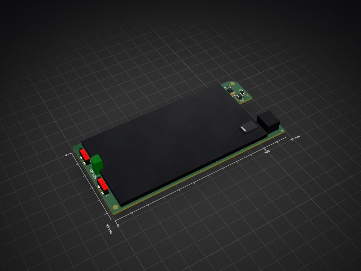
6 layers117 × 55 mmKiwiSDR PCB kiwi, the printed circuit board in 3D

KiwiSDR PCB kiwi

PCBench/PCBench21

resolution = [0.5, 0.5] pcbfolder = '../PCBs/' pcbnames = ["1Bitsy1bitsy"] iters = 30 env = PCBRoutingEnv(resolution=resolution, pcbfolder=pcbfolder, pcbnames=pcbnames) obs, info = env.reset() for in range(iters): act =…

Size
117 × 55 mm
Copper layers
6
Thickness
1.6 mm
Parts
173
Nets
119
Pads
852
Tracks, vias
1,951, 74
Routed
Yes
KiCad
KiCad 5 (file 20171130)
Created
28 Mar 2023
Updated
18 Jan 2024

Overview

KiwiSDR PCB kiwi is an open-source printed circuit board by PCBench, from the PCBench/PCBench repository on GitHub, published under the MIT licence. It is a 6-layer board of 117 × 55 mm with 173 parts on 119 nets, routed with 1,951 tracks and 74 vias.

It is built around the NC7SZ125M5, LTC2248IUH and SE4150L-R. Its parts include 94 capacitors, 19 resistors, 13 inductors, 12 ICs and 6 connectors. It belongs with the FPGA and CPLD boards of this library.

Main components

3

README

README.md

PCBench: A Dataset for Printed Circuit Board Routing

PCBench is a dataset for PCB routing task, it includes a dataset consisting of 164 printed circuit boards (PCB), a data augmentation script to expand the dataset for supervised learning (SL) tasks, and a reinforcement learning (RL) environment.

Dataset

Folder Structure

All the PCB designs in our dataset are stored in the folder PCBs, where each PCB design is stored in a subfolder named {author/org}_{PCB_name}_{design_version(optional)}. Below is the folder structure of the dataset.

text
├── PCBs
│   ├── master_metadata.json
│   ├── subfolder1
│   │   ├── raw.kicad_pcb
│   │   ├── processed.kicad_pcb
│   │   ├── final.json
│   │   ├── metadata.json
│   │   ├── visual.png
│   ├── subfolder2
│   │   ├── raw.kicad_pcb
│   │   ├── processed.kicad_pcb
│   │   ├── final.json
│   │   ├── metadata.json
│   │   ├── visual.png
│   ├── ...

The raw.kicad_pcb is the raw PCB design file, process.kicad_pcb is the file after cleaning up, final.json stores only routing-related information used for ML tasks. metadata.json stores the meta information for each single PCB design. visual.png is a visualization of each single PCB design. master_meta.json contains metadata of all PCBs and global-level information.

PCB Routing Description Language (PCB-RDL)

We propose a JSON specification (final.json for each PCB design) called the PCB Routing Description Language (PCB-RDL) that expresses a PCB routing problem and its solutions intuitively using basic concepts in order to facilitate research into automated PCB routing using ML. Following figure shows is an example of PCB with marked components in PCB-RDL (Left) and it corrsponding PCB-RDL (Right).

PCB example

Data Augmentation

Run

The augmentation data can be generated with the script Scripts/Data_augmentation/augmentation.py. To generate 3 samples by randomly extracting 50% nets from the PCB 1Bitsy_1bitsy, please run the following command

text
cd Scripts/Data_augmentation/
python augmentation.py --num_samples 3 --net_ratio 0.5 --pcb_name 1Bitsy_1bitsy

Output

All the generated PCBs will be stored in the folder named augmented_data under Scripts/Data_augmentation/. In augmented_data, all the generated samples will be stored in a subfolder with the name of selected PCB. Each generated sample has the name sample_index.json. For example, the above command will generate the following file under Scripts/Data_augmentation/

text
├── augmented_data
│   ├── 1Bitsy_1bitsy
│   │   ├── 1.json
│   │   ├── 2.json
│   │   ├── 3.json

RL environment

Installation

The RL environment requires Python >= 3.7. You can simply install the environment with the following commands:

text
git clone https://github.com/PCBench/PCBench.git
cd PCBench
python setup.py install

After installation, open a Python console and type

text
from RLEnv.EnvLayer.PCBRoutingEnv import PCBRoutingEnv

If no error occurs, you have successfully installed the PCB routing environment.

API Usage

The following content shows an example of API usage of PCBRoutingEnv.

text
from RLEnv.EnvLayer.PCBRoutingEnv import PCBRoutingEnv
import random

resolution = [0.5, 0.5]
pcb_folder = '../PCBs/'
pcb_names = ["1Bitsy_1bitsy"]
iters = 30
env = PCBRoutingEnv(resolution=resolution, pcb_folder=pcb_folder, pcb_names=pcb_names)
obs, info = env.reset()
for _ in range(iters):
    act = random.randint(0,5)
    obs, rew, terminal, _, info = env.step(act)
    if terminal:
        env.reset()

You can find more examples of customizing functions of reward and state observation from RLEnv/examples.ipynb.

Parts

173
QtyValueFootprintReferences
28470nkiwi-SM0402C1, C2, C3, C11, C12, C13, C15, C16, C23, C24, C25, C26, C30, C31, C302, C304 +12
14100nkiwi-SM0402C190, C191, C192, C195, C301, C421, C422, C423, C424, C429, C431, C433, C702, C704
114.7ukiwi-SM0402C9, C14, C17, C18, C27, C28, C34, C35, C40, C41, C706
810nkiwi-SM0402C105, C106, C193, C303, C305, C413, C417, C425
71ukiwi-SM0402C196, C197, C418, C419, C426, C427, C705
51nkiwi-SM0402C407, C409, C428, C430, C432
5FB 600Zkiwi-SM0402L102, L103, L104, L407, L408
5TEST_POINTkiwi-TP_600TP101, TP105, TP401, TP701, TP702
4100Rkiwi-SM0402R101, R102, R103, R401
4100pkiwi-SM0402C194, C408, C411, C416
4100ukiwi-SM1206C5, C20, C29, C703
410Kkiwi-SM0402R406, R409, R410, R703
4GLOBAL FIDUCIALkiwi-FIDUCIALFID3, FID4, FID5, FID6
3150nHkiwi-SM0402L403, L405, L406
32.2ukiwi-SM0402C412, C415, C420
35K6kiwi-SM0402R303, R304, R305
3TEST_POINTkiwi-TP_VIA_1250TP102, TP103, TP104
2100Rkiwi-RNET_CAY16_J8R404, R405
2160p/50kiwi-SM0402C402, C403
222pkiwi-SM0402C101, C104
2330nHkiwi-SM0402L401, L404
256p/100kiwi-SM0402C401, C404
2DNL U.FLkiwi-U.FLJ4, J5
2FPGA FIDUCIALkiwi-FIDUCIALFID1, FID2
2LP5907 3.3V 250mAkiwi-SOT23_5U104, U404
2NC7SZ125kiwi-SC70_5U403, U406
2RF_SHIELD_COVER 29x19kiwi-RF_SHIELD_COVERZR102, ZR402
2SMAkiwi-SMA_OPL_EMJ2, J3
2TEST_POINTkiwi-TP_VIA_600TP301, TP402
2TVS 3.3Vkiwi-SOD323Z401, Z402
10Rkiwi-SM0402R408
110Rkiwi-SM0402R701
116.368 MHzkiwi-TCXOX101
11n/100kiwi-SM0805C405
11uH 3.7Akiwi-INDUCTOR_4x4L701
122ukiwi-SM0805C701
1270nHkiwi-SM0402L402
128R7kiwi-SM0402R403
139nHkiwi-SM0402L101
1470n/100kiwi-SM1206C406
166.6666 MHzkiwi-XOU402
166R5kiwi-SM0402R402
16K65kiwi-SM0402R702
1Artix-7 A35kiwi-FTG256U1
1CMC 500uH 1Akiwi-CMCT301
1DNLkiwi-SM0402R407
1DNL 10nkiwi-SM0402C107
1EEPROM 32Kx8kiwi-TSSOP8U301
1HEADER 13x2kiwi-BEAGLEBONE_BLACKZB1
1LMR10530Y 1.0V 3Akiwi-WSON10U701
1LOGOkiwi-KIWI_10MMGFX1
1LP5907 1.8V 250mAkiwi-SOT23_5U702
1LTC2248kiwi-QFN32U401
1LTC6401-20kiwi-QFN16U405
1OSHWkiwi-OSHW_6MMGFX2
1POWER JACK 2.1MMkiwi-JACK_2_1MM_THJ6
1RF_SHIELD 29x19kiwi-RF_SHIELD_29x19_16PZR101
1RF_SHIELD 29x19kiwi-RF_SHIELD_29x19ZR401
1SAW L1kiwi-SAWFL101
1SE4150Lkiwi-QFN24U101
1SR 5A 40Vkiwi-DO214_AAD701
1TB_2kiwi-TB_2P_2_54MMJ1

Questions

How big is the KiwiSDR PCB kiwi PCB?

It measures 117 × 55 mm and has 6 copper layers, 1.6 mm thick.

What parts does the KiwiSDR PCB kiwi use?

173 parts, built around the NC7SZ125M5, LTC2248IUH and SE4150L-R. The full list of its parts is on this page, with links to each part's symbol and footprint where PCBKit's library has them.

Where can I download the KiwiSDR PCB kiwi KiCad files?

From the PCBench/PCBench repository on GitHub, at the commit this page was made from: the board is PCBs/KiwiSDR_PCB_kiwi/processed.kicad_pcb. PCBKit opens the board in the browser, with nothing to install.

Can I use the KiwiSDR PCB kiwi design in my own project?

Its repository publishes it under the MIT licence: you may reuse it on that licence's terms (keep the author's notice, and for a copyleft licence share your changes alike).

More from PCBench/PCBench

12
  • 2 layers398.2 × 398.2 mmLargeWordClock LargeKickstarter, the printed circuit board in 3D

    LargeWordClock LargeKickstarter

    PCBench/PCBench

    resolution = [0.5, 0.5] pcbfolder = '../PCBs/' pcbnames = ["1Bitsy1bitsy"] iters = 30 env = PCBRoutingEnv(resolution=resolution, pcbfolder=pcbfolder, pcbnames=pcbnames) obs, info = env.reset() for in range(iters): act =…

    1,591 parts21MIT
  • 4 layers95 × 95 mmRaw, the printed circuit board in 3D

    Raw

    PCBench/PCBench

    resolution = [0.5, 0.5] pcbfolder = '../PCBs/' pcbnames = ["1Bitsy1bitsy"] iters = 30 env = PCBRoutingEnv(resolution=resolution, pcbfolder=pcbfolder, pcbnames=pcbnames) obs, info = env.reset() for in range(iters): act =…

    455 parts21MIT
  • 2 layers90 × 90 mmMod12003 mod12003, the printed circuit board in 3D

    Mod12003 mod12003

    PCBench/PCBench

    resolution = [0.5, 0.5] pcbfolder = '../PCBs/' pcbnames = ["1Bitsy1bitsy"] iters = 30 env = PCBRoutingEnv(resolution=resolution, pcbfolder=pcbfolder, pcbnames=pcbnames) obs, info = env.reset() for in range(iters): act =…

    452 parts21MIT
  • 2 layers88.9 × 114.3 mmRaw, the printed circuit board in 3D

    Raw

    PCBench/PCBench

    resolution = [0.5, 0.5] pcbfolder = '../PCBs/' pcbnames = ["1Bitsy1bitsy"] iters = 30 env = PCBRoutingEnv(resolution=resolution, pcbfolder=pcbfolder, pcbnames=pcbnames) obs, info = env.reset() for in range(iters): act =…

    190 parts21MIT
  • 2 layers100 × 100 mmMod1base mod1base, the printed circuit board in 3D

    Mod1base mod1base

    PCBench/PCBench

    resolution = [0.5, 0.5] pcbfolder = '../PCBs/' pcbnames = ["1Bitsy1bitsy"] iters = 30 env = PCBRoutingEnv(resolution=resolution, pcbfolder=pcbfolder, pcbnames=pcbnames) obs, info = env.reset() for in range(iters): act =…

    187 parts21MIT
  • 4 layers143 × 74 mmKitspace lpa96, the printed circuit board in 3D

    Kitspace lpa96

    PCBench/PCBench

    resolution = [0.5, 0.5] pcbfolder = '../PCBs/' pcbnames = ["1Bitsy1bitsy"] iters = 30 env = PCBRoutingEnv(resolution=resolution, pcbfolder=pcbfolder, pcbnames=pcbnames) obs, info = env.reset() for in range(iters): act =…

    161 parts21MIT
  • 2 layers101.6 × 99.7 mmRaw, the printed circuit board in 3D

    Raw

    PCBench/PCBench

    resolution = [0.5, 0.5] pcbfolder = '../PCBs/' pcbnames = ["1Bitsy1bitsy"] iters = 30 env = PCBRoutingEnv(resolution=resolution, pcbfolder=pcbfolder, pcbnames=pcbnames) obs, info = env.reset() for in range(iters): act =…

    158 parts21MIT
  • 4 layers36.1 × 32.7 mmKitspace tri panel 4up r0.1, the printed circuit board in 3D

    Kitspace tri panel 4up r0.1

    PCBench/PCBench

    resolution = [0.5, 0.5] pcbfolder = '../PCBs/' pcbnames = ["1Bitsy1bitsy"] iters = 30 env = PCBRoutingEnv(resolution=resolution, pcbfolder=pcbfolder, pcbnames=pcbnames) obs, info = env.reset() for in range(iters): act =…

    157 parts21MIT
  • 2 layers101.6 × 99.7 mmKarabas nano karabas nano revB, the printed circuit board in 3D

    Karabas nano karabas nano revB

    PCBench/PCBench

    resolution = [0.5, 0.5] pcbfolder = '../PCBs/' pcbnames = ["1Bitsy1bitsy"] iters = 30 env = PCBRoutingEnv(resolution=resolution, pcbfolder=pcbfolder, pcbnames=pcbnames) obs, info = env.reset() for in range(iters): act =…

    147 parts21MIT
  • 4 layers65 × 60 mmReworkctf reworkctf, the printed circuit board in 3D

    Reworkctf reworkctf

    PCBench/PCBench

    resolution = [0.5, 0.5] pcbfolder = '../PCBs/' pcbnames = ["1Bitsy1bitsy"] iters = 30 env = PCBRoutingEnv(resolution=resolution, pcbfolder=pcbfolder, pcbnames=pcbnames) obs, info = env.reset() for in range(iters): act =…

    143 parts21MIT
  • 2 layers99.1 × 99.1 mmRaw, the printed circuit board in 3D

    Raw

    PCBench/PCBench

    resolution = [0.5, 0.5] pcbfolder = '../PCBs/' pcbnames = ["1Bitsy1bitsy"] iters = 30 env = PCBRoutingEnv(resolution=resolution, pcbfolder=pcbfolder, pcbnames=pcbnames) obs, info = env.reset() for in range(iters): act =…

    77 parts21MIT
  • 2 layers645.9 × 78.2 mmAnalog esr meter esr meter rev a, the printed circuit board in 3D

    Analog esr meter esr meter rev a

    PCBench/PCBench

    resolution = [0.5, 0.5] pcbfolder = '../PCBs/' pcbnames = ["1Bitsy1bitsy"] iters = 30 env = PCBRoutingEnv(resolution=resolution, pcbfolder=pcbfolder, pcbnames=pcbnames) obs, info = env.reset() for in range(iters): act =…

    71 parts21MIT

Similar boards

  • 4 layers42.8 × 36.8 mmDriver board, the printed circuit board in 3D

    Driver board

    blazer82/FT81x_Arduino_Driver

    FT81x on ST7701S Arduino Driver

    49 parts59MIT
  • 4 layers119.5 × 75.3 mmTimingMonitor, the printed circuit board in 3D

    TimingMonitor

    lwa-project/zcu102_timing_monitor

    Board to power/monitor the clock distribution to ZCU102 boards

    102 parts1
  • 4 layers160 × 100 mmETH1CJTAG, the printed circuit board in 3D

    ETH1CJTAG

    BehrensG/ETH1CJTAG

    Low cost JTAG

    478 partsGPL-3.0
  • 6 layers50 × 50 mmEcatExBrd, the printed circuit board in 3D

    EcatExBrd

    open-dynamic-robot-initiative/open-motor-driver-initiative

    Open-source drive for brushless motors, following the open dynamic robot initiative

    173 parts122BSD-3-Clause
  • 6 layers39.5 × 39.5 mmLEVIA H7, the printed circuit board in 3D

    LEVIA H7

    piecol/LEVIA-H7

    Open hardware STM32H743 drone flight controller

    173 parts71CERN-OHL-S-2.0
  • 6 layers65.6 × 55 mmCameraPCB, the printed circuit board in 3D

    CameraPCB

    JackkP/Semi-Truck-Backup-Camera

    Repository for Team 25 Purdue ECE Senior Design Fall 2025 49022 Senior Design Project. This contains all of the code and schematics for the project. Course-related documentation is stored in google.
    173 parts1
  • 6 layers122 × 61.5 mmGc20140203 v2, the printed circuit board in 3D

    Gc20140203 v2

    masahirosuzuka/GameChanger

    Open Source Hardware Tablet PC

    173 parts1
  • 6 layers253.6 × 134.2 mmCadzilla, the printed circuit board in 3D

    Cadzilla

    ToddHoug/cadzilla

    CADzilla is an S-100 bus board built around the Hitachi HD63484 Advanced CRT Controller (ACRTC) paired with a Brooktree Bt453 video DAC.

    172 parts