Skip to the content
PCBKitNew board
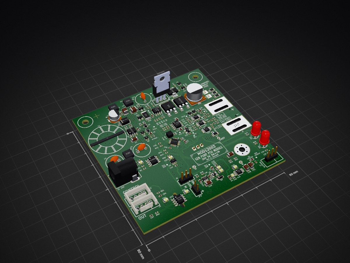
2 layers90 × 90 mmMod12003 mod12003, the printed circuit board in 3D

Mod12003 mod12003

PCBench/PCBench21

resolution = [0.5, 0.5] pcbfolder = '../PCBs/' pcbnames = ["1Bitsy1bitsy"] iters = 30 env = PCBRoutingEnv(resolution=resolution, pcbfolder=pcbfolder, pcbnames=pcbnames) obs, info = env.reset() for in range(iters): act =…

Size
90 × 90 mm
Copper layers
2
Thickness
1.6 mm
Parts
452
Nets
100
Pads
758
Tracks, vias
2,210, 85
Routed
Yes
KiCad
KiCad 5 (file 20171130)
Created
28 Mar 2023
Updated
18 Jan 2024

Overview

Mod12003 mod12003 is an open-source printed circuit board by PCBench, from the PCBench/PCBench repository on GitHub, published under the MIT licence. It is a 2-layer board of 90 × 90 mm with 452 parts on 100 nets, routed with 2,210 tracks and 85 vias.

It is built around the ATXMEGA32E5-M4U, LM358DGK and AOZ1282CI, with the MAX5215GUA+, MCP9701-E/TO and OPA2376AIDGK among its other parts. Its parts include 59 capacitors, 53 resistors, 12 ICs, 12 transistors and 8 connectors. It belongs with the AVR (ATmega, ATtiny) boards of this library.

Main components

12

README

README.md

PCBench: A Dataset for Printed Circuit Board Routing

PCBench is a dataset for PCB routing task, it includes a dataset consisting of 164 printed circuit boards (PCB), a data augmentation script to expand the dataset for supervised learning (SL) tasks, and a reinforcement learning (RL) environment.

Dataset

Folder Structure

All the PCB designs in our dataset are stored in the folder PCBs, where each PCB design is stored in a subfolder named {author/org}_{PCB_name}_{design_version(optional)}. Below is the folder structure of the dataset.

text
├── PCBs
│   ├── master_metadata.json
│   ├── subfolder1
│   │   ├── raw.kicad_pcb
│   │   ├── processed.kicad_pcb
│   │   ├── final.json
│   │   ├── metadata.json
│   │   ├── visual.png
│   ├── subfolder2
│   │   ├── raw.kicad_pcb
│   │   ├── processed.kicad_pcb
│   │   ├── final.json
│   │   ├── metadata.json
│   │   ├── visual.png
│   ├── ...

The raw.kicad_pcb is the raw PCB design file, process.kicad_pcb is the file after cleaning up, final.json stores only routing-related information used for ML tasks. metadata.json stores the meta information for each single PCB design. visual.png is a visualization of each single PCB design. master_meta.json contains metadata of all PCBs and global-level information.

PCB Routing Description Language (PCB-RDL)

We propose a JSON specification (final.json for each PCB design) called the PCB Routing Description Language (PCB-RDL) that expresses a PCB routing problem and its solutions intuitively using basic concepts in order to facilitate research into automated PCB routing using ML. Following figure shows is an example of PCB with marked components in PCB-RDL (Left) and it corrsponding PCB-RDL (Right).

PCB example

Data Augmentation

Run

The augmentation data can be generated with the script Scripts/Data_augmentation/augmentation.py. To generate 3 samples by randomly extracting 50% nets from the PCB 1Bitsy_1bitsy, please run the following command

text
cd Scripts/Data_augmentation/
python augmentation.py --num_samples 3 --net_ratio 0.5 --pcb_name 1Bitsy_1bitsy

Output

All the generated PCBs will be stored in the folder named augmented_data under Scripts/Data_augmentation/. In augmented_data, all the generated samples will be stored in a subfolder with the name of selected PCB. Each generated sample has the name sample_index.json. For example, the above command will generate the following file under Scripts/Data_augmentation/

text
├── augmented_data
│   ├── 1Bitsy_1bitsy
│   │   ├── 1.json
│   │   ├── 2.json
│   │   ├── 3.json

RL environment

Installation

The RL environment requires Python >= 3.7. You can simply install the environment with the following commands:

text
git clone https://github.com/PCBench/PCBench.git
cd PCBench
python setup.py install

After installation, open a Python console and type

text
from RLEnv.EnvLayer.PCBRoutingEnv import PCBRoutingEnv

If no error occurs, you have successfully installed the PCB routing environment.

API Usage

The following content shows an example of API usage of PCBRoutingEnv.

text
from RLEnv.EnvLayer.PCBRoutingEnv import PCBRoutingEnv
import random

resolution = [0.5, 0.5]
pcb_folder = '../PCBs/'
pcb_names = ["1Bitsy_1bitsy"]
iters = 30
env = PCBRoutingEnv(resolution=resolution, pcb_folder=pcb_folder, pcb_names=pcb_names)
obs, info = env.reset()
for _ in range(iters):
    act = random.randint(0,5)
    obs, rew, terminal, _, info = env.step(act)
    if terminal:
        env.reset()

You can find more examples of customizing functions of reward and state observation from RLEnv/examples.ipynb.

Parts

452
QtyValueFootprintReferences
92VIA-0.8mmVIA-0.8mmVIA11, VIA12, VIA21, VIA22, VIA311, VIA3111, VIA3111_2, VIA3111_3, VIA3112, VIA3112_10, VIA3112_11, VIA3112_12, VIA3112_13, VIA3112_14, VIA3112_15, VIA3112_16 +76
19100nIPC7351-Nominal:CAPC1005X55C3, C19, C20, C21, C23, C31, C32, C33, C34, C35, C36, C37, C38, C39, C45, C47 +3
192kIPC7351-Nominal:RESC1005X40R10, R13, R14, R17, R18, R19, R20, R26, R27, R31, R33, R36, R43, R46, R47, R49 +3
1122kIPC7351-Nominal:RESC1005X40R7, R15, R16, R21, R23, R24, R25, R29, R30, R39, R42
9100nIPC7351-Nominal:CAPC1608X55C8, C9, C12, C14, C22, C24, C26, C41, C42
8470kIPC7351-Nominal:RESC1005X40R1, R2, R34, R35, R38, R41, R52, R53
722nIPC7351-Nominal:CAPC1005X55C2, C17, C18, C25, C27, C29, C30
6120IPC7351-Nominal:INDC1608X95E1, E2, E3, E4, E5, E6
6348IPC7351-Nominal:RESC1005X40R4, R22, R32, R37, R44, R45
54u7IPC7351-Nominal:CAPC2012X70C43, C44, C46, C49, C50
4100IPC7351-Nominal:RESC1005X40R11, R12, R40, R51
4220pIPC7351-Nominal:CAPC1005X55C10, C28, C54, C57
31kIPC7351-Nominal:RESC6432X70R5, R6, R28
31uIPC7351-Nominal:CAPC2012X70C1, C55, C56
33u3manuf:BOURNS-SRN5040L1, L3, L4
3470upth-passive:C-ALUM-10mmC5, C6, C16
34AIPC7351-Nominal:RESC3216X60F1, F2, F3
3NET-TIEconn-test:NET-TIE-0.3mmW1, W2, W3
3SCREWmech:SCREW-4-SUPPORTEDMP1, MP2, MP3
21uIPC7351-Nominal:CAPC3225X88C13, C15
222uIPC7351-Nominal:CAPC3216X70C48, C51
23904smd-semi:SC-70Q3, Q4
24403smd-semi:SC-70Q5, Q6
26u8IPC7351-Nominal:CAPC3216X70C7, C40
2AO4805IPC7351-Nominal:SOIC127P600X175-8Q1, Q7
2BAT54AWTsmd-semi:SC-70D3, D4
2JUMPER-SOLDERconn-test:JUMPER-SOLDER-3mmJP1, JP2
2LM393MIPC7351-Nominal:SOIC127P600X175-8U3, U4
1-230mVconn-test:TEST-SMD-SMALLTP5
1100uL1L2
112Asmd-semi:TO-252Q2
11n/1kVIPC7351-Nominal:CAPC3216X70C58
122umanuf:BOURNS-SRN3015L5
124Vconn-cui:CONN-PJ-037AJ3
12N7002PWsmd-semi:SC-70Q9
12V048conn-test:TEST-SMD-SMALLTP2
1330uIPC7351-Nominal:CAPAE1030X1250C4
133uIPC7351-Nominal:CAPAE660X570C11
13V3conn-test:TEST-SMD-SMALLTP4
13V6conn-test:TEST-SMD-SMALLTP3
140V/5Asmd-semi:TO-252D1
14403smd-semi:SOT-23Q8
16k98IPC7351-Nominal:RESC1005X40R48
184B24smd-semi:SOT-23DZ1
1ADR380smd-semi:SOT-23U7
1AOZ1282smd-semi:SOT-23-6U8
1ATXMEGA32E5-M4Usmd-semi:QFN40P400X400X55-33U5
1BUTTONSconn-100mil:CONN-100MIL-M-1x3-SHROUDJ7
1CCpth-semi:LED-5mmDS2
1CVpth-semi:LED-5mmDS1
1D45H11pth-semi:TO-220Q10
1DEVELconn-100mil:CONN-100MIL-M-1x3J8
1DRIVEconn-test:TEST-SMD-SMALLTP13
1IDRIVEconn-test:TEST-SMD-SMALLTP12
1INconn-100mil:CONN-100MIL-M-1x4-SHROUDJ1
1ISENSEconn-test:TEST-SMD-SMALLTP9
1ISETconn-test:TEST-SMD-SMALLTP10
1JUMPERconn-100mil:CONN-100MIL-M-1x2JP3
1LM358DGKIPC7351-Nominal:SOP65P490X110-8U2
1LM7705IPC7351-Nominal:SOP65P490X110-8U10
1MAX5215IPC7351-Nominal:SOP65P490X110-8U11
1MBR0530smd-semi:SOD-123D5
1MBRS360BIPC7351-Nominal:DIOM5436X244D2
1MCP9701-E/TOconn-100mil:CONN-100MIL-M-1x3U6
1OPA2376AIDGKIPC7351-Nominal:SOP65P490X110-8U1
1OUTconn-100mil:CONN-100MIL-M-1x4-SHROUDJ2
1OUT+J1J4
1OUT-J1J5
1OVP_THconn-test:TEST-SMD-SMALLTP6
1PDIconn-100mil:CONN-100MIL-M-2x3J6
1PMSS3904smd-semi:SC-70Q11
1PREREGconn-test:TEST-SMD-SMALLTP1
1PZT3904smd-semi:SOT-223Q12
1R010IPC7351-Nominal:RESC3216X60R3
1SWconn-test:TEST-SMD-SMALLTP14
1Si8421IPC7351-Nominal:SOIC127P600X175-8U12
1TLV70233DBVsmd-semi:SOT-23-5U9
1VDRIVEconn-test:TEST-SMD-SMALLTP11
1VSENSEconn-test:TEST-SMD-SMALLTP7
1VSETconn-test:TEST-SMD-SMALLTP8

The 281 most common of 452 parts.

Questions

How big is the Mod12003 mod12003 PCB?

It measures 90 × 90 mm and has 2 copper layers, 1.6 mm thick.

What parts does the Mod12003 mod12003 use?

452 parts, built around the ATXMEGA32E5-M4U, LM358DGK, AOZ1282CI and MAX5215GUA+. The full list of its parts is on this page, with links to each part's symbol and footprint where PCBKit's library has them.

Where can I download the Mod12003 mod12003 KiCad files?

From the PCBench/PCBench repository on GitHub, at the commit this page was made from: the board is PCBs/mod12003_mod12003/processed.kicad_pcb. PCBKit opens the board in the browser, with nothing to install.

Can I use the Mod12003 mod12003 design in my own project?

Its repository publishes it under the MIT licence: you may reuse it on that licence's terms (keep the author's notice, and for a copyleft licence share your changes alike).
More from PCBench/PCBench

12
  • 2 layers398.2 × 398.2 mmLargeWordClock LargeKickstarter, the printed circuit board in 3D

    LargeWordClock LargeKickstarter

    PCBench/PCBench

    resolution = [0.5, 0.5] pcbfolder = '../PCBs/' pcbnames = ["1Bitsy1bitsy"] iters = 30 env = PCBRoutingEnv(resolution=resolution, pcbfolder=pcbfolder, pcbnames=pcbnames) obs, info = env.reset() for in range(iters): act =…

    1,591 parts21MIT
  • 4 layers95 × 95 mmRaw, the printed circuit board in 3D

    Raw

    PCBench/PCBench

    resolution = [0.5, 0.5] pcbfolder = '../PCBs/' pcbnames = ["1Bitsy1bitsy"] iters = 30 env = PCBRoutingEnv(resolution=resolution, pcbfolder=pcbfolder, pcbnames=pcbnames) obs, info = env.reset() for in range(iters): act =…

    455 parts21MIT
  • 2 layers88.9 × 114.3 mmRaw, the printed circuit board in 3D

    Raw

    PCBench/PCBench

    resolution = [0.5, 0.5] pcbfolder = '../PCBs/' pcbnames = ["1Bitsy1bitsy"] iters = 30 env = PCBRoutingEnv(resolution=resolution, pcbfolder=pcbfolder, pcbnames=pcbnames) obs, info = env.reset() for in range(iters): act =…

    190 parts21MIT
  • 2 layers100 × 100 mmMod1base mod1base, the printed circuit board in 3D

    Mod1base mod1base

    PCBench/PCBench

    resolution = [0.5, 0.5] pcbfolder = '../PCBs/' pcbnames = ["1Bitsy1bitsy"] iters = 30 env = PCBRoutingEnv(resolution=resolution, pcbfolder=pcbfolder, pcbnames=pcbnames) obs, info = env.reset() for in range(iters): act =…

    187 parts21MIT
  • 6 layers117 × 55 mmKiwiSDR PCB kiwi, the printed circuit board in 3D

    KiwiSDR PCB kiwi

    PCBench/PCBench

    resolution = [0.5, 0.5] pcbfolder = '../PCBs/' pcbnames = ["1Bitsy1bitsy"] iters = 30 env = PCBRoutingEnv(resolution=resolution, pcbfolder=pcbfolder, pcbnames=pcbnames) obs, info = env.reset() for in range(iters): act =…

    173 parts21MIT
  • 4 layers143 × 74 mmKitspace lpa96, the printed circuit board in 3D

    Kitspace lpa96

    PCBench/PCBench

    resolution = [0.5, 0.5] pcbfolder = '../PCBs/' pcbnames = ["1Bitsy1bitsy"] iters = 30 env = PCBRoutingEnv(resolution=resolution, pcbfolder=pcbfolder, pcbnames=pcbnames) obs, info = env.reset() for in range(iters): act =…

    161 parts21MIT
  • 2 layers101.6 × 99.7 mmRaw, the printed circuit board in 3D

    Raw

    PCBench/PCBench

    resolution = [0.5, 0.5] pcbfolder = '../PCBs/' pcbnames = ["1Bitsy1bitsy"] iters = 30 env = PCBRoutingEnv(resolution=resolution, pcbfolder=pcbfolder, pcbnames=pcbnames) obs, info = env.reset() for in range(iters): act =…

    158 parts21MIT
  • 4 layers36.1 × 32.7 mmKitspace tri panel 4up r0.1, the printed circuit board in 3D

    Kitspace tri panel 4up r0.1

    PCBench/PCBench

    resolution = [0.5, 0.5] pcbfolder = '../PCBs/' pcbnames = ["1Bitsy1bitsy"] iters = 30 env = PCBRoutingEnv(resolution=resolution, pcbfolder=pcbfolder, pcbnames=pcbnames) obs, info = env.reset() for in range(iters): act =…

    157 parts21MIT
  • 2 layers101.6 × 99.7 mmKarabas nano karabas nano revB, the printed circuit board in 3D

    Karabas nano karabas nano revB

    PCBench/PCBench

    resolution = [0.5, 0.5] pcbfolder = '../PCBs/' pcbnames = ["1Bitsy1bitsy"] iters = 30 env = PCBRoutingEnv(resolution=resolution, pcbfolder=pcbfolder, pcbnames=pcbnames) obs, info = env.reset() for in range(iters): act =…

    147 parts21MIT
  • 4 layers65 × 60 mmReworkctf reworkctf, the printed circuit board in 3D

    Reworkctf reworkctf

    PCBench/PCBench

    resolution = [0.5, 0.5] pcbfolder = '../PCBs/' pcbnames = ["1Bitsy1bitsy"] iters = 30 env = PCBRoutingEnv(resolution=resolution, pcbfolder=pcbfolder, pcbnames=pcbnames) obs, info = env.reset() for in range(iters): act =…

    143 parts21MIT
  • 2 layers99.1 × 99.1 mmRaw, the printed circuit board in 3D

    Raw

    PCBench/PCBench

    resolution = [0.5, 0.5] pcbfolder = '../PCBs/' pcbnames = ["1Bitsy1bitsy"] iters = 30 env = PCBRoutingEnv(resolution=resolution, pcbfolder=pcbfolder, pcbnames=pcbnames) obs, info = env.reset() for in range(iters): act =…

    77 parts21MIT
  • 2 layers645.9 × 78.2 mmAnalog esr meter esr meter rev a, the printed circuit board in 3D

    Analog esr meter esr meter rev a

    PCBench/PCBench

    resolution = [0.5, 0.5] pcbfolder = '../PCBs/' pcbnames = ["1Bitsy1bitsy"] iters = 30 env = PCBRoutingEnv(resolution=resolution, pcbfolder=pcbfolder, pcbnames=pcbnames) obs, info = env.reset() for in range(iters): act =…

    71 parts21MIT

Similar boards

  • 4 layers160 × 90 mmVESC controller, the printed circuit board in 3D

    VESC controller

    paltatech/VESC-controller

    Made open source with KiCAD, an open source EDA tool.

    342 parts356
  • 2 layers68.6 × 53.4 mmWize shield, the printed circuit board in 3D

    Wize shield

    AllWize/AllWizeK1-hardware

    hardware files

    53 parts3LGPL-2.1
  • 2 layers53.5 × 101.8 mmSony scopeman, the printed circuit board in 3D

    Sony scopeman

    lucysrausch/sony-scopeman

    Hardware Design files of a replacement mainboard for the Sony Watchman FD-10. This turns it into a bluetooth and WiFi-enabled vector display.

    135 parts69
  • 4 layers65 × 35 mmFlexiBMS, the printed circuit board in 3D

    FlexiBMS

    SimosMCmuffin/FlexiBMS_hardware

    Open Source BMS developed by Simo Sihvonen (Simos MCmuffin) with the Esk8 community, for the Esk8 community

    209 parts14
  • 2 layers75.7 × 37.4 mmSpectrometer, the printed circuit board in 3D

    Spectrometer

    atx/spectrometer

    Alpha spectrometer developed during my internship at the Institute at the Experimental and Applied Physics

    270 parts2MIT
  • 4 layers91.9 × 53.2 mmPhoenix main board, the printed circuit board in 3D

    Phoenix main board

    Phalkon-Industries/phoenix-instrument

    Git repo for the content of the new Phoenix ph handheld instrument.

    117 parts2CERN-OHL-S-2.0
  • 2 layers100 × 100 mmVH3, the printed circuit board in 3D

    VH3

    laurapellizari/PBLE01---Hardware

    Embedded hardware design for learning

    90 parts