Skip to the content
PCBKitNew board
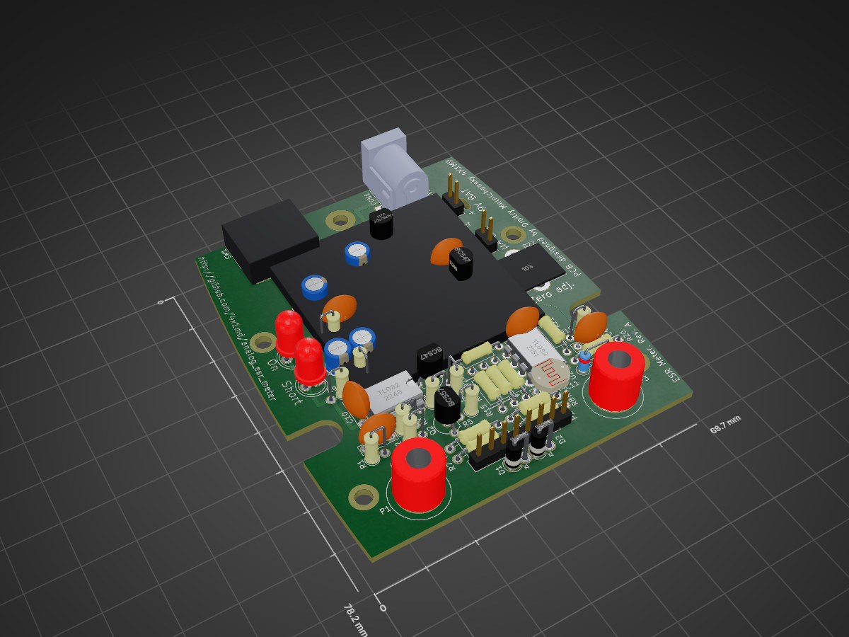
2 layers645.9 × 78.2 mmAnalog esr meter esr meter rev a, the printed circuit board in 3D

Analog esr meter esr meter rev a

PCBench/PCBench21

resolution = [0.5, 0.5] pcbfolder = '../PCBs/' pcbnames = ["1Bitsy1bitsy"] iters = 30 env = PCBRoutingEnv(resolution=resolution, pcbfolder=pcbfolder, pcbnames=pcbnames) obs, info = env.reset() for in range(iters): act =…

Size
645.9 × 78.2 mm
Copper layers
2
Thickness
1.6 mm
Parts
71
Nets
30
Pads
151
Tracks, vias
222, 0
Routed
Yes
KiCad
KiCad 5 (file 20171130)
Created
28 Mar 2023
Updated
18 Jan 2024

Overview

Analog esr meter esr meter rev a is an open-source printed circuit board by PCBench, from the PCBench/PCBench repository on GitHub, published under the MIT licence. It is a 2-layer board of 645.9 × 78.2 mm with 71 parts on 30 nets, routed with 222 tracks and 0 vias.

It is built around the TL082, LM7809CT and BC547, with the BC557 among its other parts. Its parts include 23 resistors, 11 capacitors, 6 diodes, 6 connectors and 3 ICs.

Main components

4

README

README.md

PCBench: A Dataset for Printed Circuit Board Routing

PCBench is a dataset for PCB routing task, it includes a dataset consisting of 164 printed circuit boards (PCB), a data augmentation script to expand the dataset for supervised learning (SL) tasks, and a reinforcement learning (RL) environment.

Dataset

Folder Structure

All the PCB designs in our dataset are stored in the folder PCBs, where each PCB design is stored in a subfolder named {author/org}_{PCB_name}_{design_version(optional)}. Below is the folder structure of the dataset.

text
├── PCBs
│   ├── master_metadata.json
│   ├── subfolder1
│   │   ├── raw.kicad_pcb
│   │   ├── processed.kicad_pcb
│   │   ├── final.json
│   │   ├── metadata.json
│   │   ├── visual.png
│   ├── subfolder2
│   │   ├── raw.kicad_pcb
│   │   ├── processed.kicad_pcb
│   │   ├── final.json
│   │   ├── metadata.json
│   │   ├── visual.png
│   ├── ...

The raw.kicad_pcb is the raw PCB design file, process.kicad_pcb is the file after cleaning up, final.json stores only routing-related information used for ML tasks. metadata.json stores the meta information for each single PCB design. visual.png is a visualization of each single PCB design. master_meta.json contains metadata of all PCBs and global-level information.

PCB Routing Description Language (PCB-RDL)

We propose a JSON specification (final.json for each PCB design) called the PCB Routing Description Language (PCB-RDL) that expresses a PCB routing problem and its solutions intuitively using basic concepts in order to facilitate research into automated PCB routing using ML. Following figure shows is an example of PCB with marked components in PCB-RDL (Left) and it corrsponding PCB-RDL (Right).

PCB example

Data Augmentation

Run

The augmentation data can be generated with the script Scripts/Data_augmentation/augmentation.py. To generate 3 samples by randomly extracting 50% nets from the PCB 1Bitsy_1bitsy, please run the following command

text
cd Scripts/Data_augmentation/
python augmentation.py --num_samples 3 --net_ratio 0.5 --pcb_name 1Bitsy_1bitsy

Output

All the generated PCBs will be stored in the folder named augmented_data under Scripts/Data_augmentation/. In augmented_data, all the generated samples will be stored in a subfolder with the name of selected PCB. Each generated sample has the name sample_index.json. For example, the above command will generate the following file under Scripts/Data_augmentation/

text
├── augmented_data
│   ├── 1Bitsy_1bitsy
│   │   ├── 1.json
│   │   ├── 2.json
│   │   ├── 3.json

RL environment

Installation

The RL environment requires Python >= 3.7. You can simply install the environment with the following commands:

text
git clone https://github.com/PCBench/PCBench.git
cd PCBench
python setup.py install

After installation, open a Python console and type

text
from RLEnv.EnvLayer.PCBRoutingEnv import PCBRoutingEnv

If no error occurs, you have successfully installed the PCB routing environment.

API Usage

The following content shows an example of API usage of PCBRoutingEnv.

text
from RLEnv.EnvLayer.PCBRoutingEnv import PCBRoutingEnv
import random

resolution = [0.5, 0.5]
pcb_folder = '../PCBs/'
pcb_names = ["1Bitsy_1bitsy"]
iters = 30
env = PCBRoutingEnv(resolution=resolution, pcb_folder=pcb_folder, pcb_names=pcb_names)
obs, info = env.reset()
for _ in range(iters):
    act = random.randint(0,5)
    obs, rew, terminal, _, info = env.step(act)
    if terminal:
        env.reset()

You can find more examples of customizing functions of reward and state observation from RLEnv/examples.ipynb.

Parts

71
QtyValueFootprintReferences
51KResistors_THT:R_Axial_DIN0207_L6.3mm_D2.5mm_P10.16mm_HorizontalR7, R11, R13, R14, R21
53.2mm_M3_DIN965Mounting_Holes:MountingHole_3.2mm_M3_DIN965MH1, MH2, MH3, MH4, MH5
40.1uFCapacitors_THT:C_Rect_L7.0mm_W2.0mm_P5.00mmC3, C7, C10, C11
410KResistors_THT:R_Axial_DIN0207_L6.3mm_D2.5mm_P2.54mm_VerticalR2, R3, R9, R10
21N4001Diodes_THT:D_DO-41_SOD81_P2.54mm_Vertical_AnodeUpD1, D2
21uFCapacitors_THT:CP_Radial_D5.0mm_P2.50mmC5, C6
21uFCapacitors_THT:C_Rect_L7.0mm_W2.0mm_P5.00mmC2, C4
222Resistors_THT:R_Axial_DIN0207_L6.3mm_D2.5mm_P10.16mm_HorizontalR8, R12
247KResistors_THT:R_Axial_DIN0207_L6.3mm_D2.5mm_P10.16mm_HorizontalR15, R16
2BC547TO_SOT_Packages_THT:TO-92_Inline_WideQ1, Q3
2TL082Housings_DIP:DIP-8_W7.62mmU1, U2
1+4.5VMeasurement_Points:Measurement_Point_Round-SMD-Pad_SmallTP7
1+9V regMeasurement_Points:Measurement_Point_Round-SMD-Pad_SmallTP9
1-4.5VMeasurement_Points:Measurement_Point_Round-SMD-Pad_SmallTP8
11.5KResistors_THT:R_Axial_DIN0207_L6.3mm_D2.5mm_P2.54mm_VerticalR1
11.5mmx3.2mm_hole_for_wiresESR_Meter_Footprints:1.5mmx3.2mm_hole_for_wiresMH**
110KPotentiometers:Potentiometer_Alps_RK09K_HorizontalR22
110uFCapacitors_THT:CP_Radial_D5.0mm_P2.50mmC9
112KResistors_THT:R_Axial_DIN0207_L6.3mm_D2.5mm_P2.54mm_VerticalR6
115KResistors_THT:R_Axial_DIN0207_L6.3mm_D2.5mm_P10.16mm_HorizontalR17
11N4148Diodes_THT:D_DO-35_SOD27_P5.08mm_Vertical_KathodeUpD5
11nFCapacitors_THT:C_Rect_L7.0mm_W2.0mm_P5.00mmC1
122uFCapacitors_THT:CP_Radial_D5.0mm_P2.50mmC8
14.7KResistors_THT:R_Axial_DIN0207_L6.3mm_D2.5mm_P2.54mm_VerticalR5
147Resistors_THT:R_Axial_DIN0207_L6.3mm_D2.5mm_P10.16mm_HorizontalR20
1470Resistors_THT:R_Axial_DIN0207_L6.3mm_D2.5mm_P10.16mm_HorizontalR18
1470Resistors_THT:R_Axial_DIN0207_L6.3mm_D2.5mm_P2.54mm_VerticalR23
147KResistors_THT:R_Axial_DIN0207_L6.3mm_D2.5mm_P2.54mm_VerticalR19
150-250uAESR_Meter_Footprints:MicroampermeterPA1
168KResistors_THT:R_Axial_DIN0207_L6.3mm_D2.5mm_P2.54mm_VerticalR4
19V batteryPin_Headers:Pin_Header_Straight_1x02_Pitch2.54mmP4
1Amp (-)Measurement_Points:Measurement_Point_Round-SMD-Pad_SmallTP4
1Amp. (+)Measurement_Points:Measurement_Point_Round-SMD-Pad_SmallTP3
1Amp. outMeasurement_Points:Measurement_Point_Round-SMD-Pad_SmallTP5
1BAT60Diodes_THT:D_DO-35_SOD27_P7.62mm_HorizontalD4
1BC557TO_SOT_Packages_THT:TO-92_Inline_WideQ2
1BridgeMeasurement_Points:Measurement_Point_Round-SMD-Pad_SmallTP2
1CxSocket_Strips:Socket_Strip_Straight_1x08_Pitch2.54mmP2
1Cx+ESR_Meter_Footprints:Banana_Jack_1PinP1
1Cx-ESR_Meter_Footprints:Banana_Jack_1PinP3
1External powerESR_Meter_Footprints:BARREL_JACK_PCB_EDGECON1
1GNDMeasurement_Points:Measurement_Point_Round-SMD-Pad_SmallTP6
1GreenLEDs:LED_D5.0mmD6
1LM7809CTTO_SOT_Packages_THT:TO-92_Molded_Wide_OvalU3
1On/OffESR_Meter_Footprints:Switch_Slide_SPDT_THT_5MS1S102AM6QESSW1
1Osc. outMeasurement_Points:Measurement_Point_Round-SMD-Pad_SmallTP1
1RedLEDs:LED_D5.0mmD3
1VoutMeasurement_Points:Measurement_Point_Round-SMD-Pad_SmallTP10
1uA connectorPin_Headers:Pin_Header_Straight_1x02_Pitch2.54mmP5

The 70 most common of 71 parts.

Questions

How big is the Analog esr meter esr meter rev a PCB?

It measures 645.9 × 78.2 mm and has 2 copper layers, 1.6 mm thick.

What parts does the Analog esr meter esr meter rev a use?

71 parts, built around the TL082, LM7809CT, BC547 and BC557. The full list of its parts is on this page, with links to each part's symbol and footprint where PCBKit's library has them.

Where can I download the Analog esr meter esr meter rev a KiCad files?

From the PCBench/PCBench repository on GitHub, at the commit this page was made from: the board is PCBs/analog_esr_meter_esr_meter_rev_a/processed.kicad_pcb. PCBKit opens the board in the browser, with nothing to install.

Can I use the Analog esr meter esr meter rev a design in my own project?

Its repository publishes it under the MIT licence: you may reuse it on that licence's terms (keep the author's notice, and for a copyleft licence share your changes alike).

More from PCBench/PCBench

12
  • 2 layers398.2 × 398.2 mmLargeWordClock LargeKickstarter, the printed circuit board in 3D

    LargeWordClock LargeKickstarter

    PCBench/PCBench

    resolution = [0.5, 0.5] pcbfolder = '../PCBs/' pcbnames = ["1Bitsy1bitsy"] iters = 30 env = PCBRoutingEnv(resolution=resolution, pcbfolder=pcbfolder, pcbnames=pcbnames) obs, info = env.reset() for in range(iters): act =…

    1,591 parts21MIT
  • 4 layers95 × 95 mmRaw, the printed circuit board in 3D

    Raw

    PCBench/PCBench

    resolution = [0.5, 0.5] pcbfolder = '../PCBs/' pcbnames = ["1Bitsy1bitsy"] iters = 30 env = PCBRoutingEnv(resolution=resolution, pcbfolder=pcbfolder, pcbnames=pcbnames) obs, info = env.reset() for in range(iters): act =…

    455 parts21MIT
  • 2 layers90 × 90 mmMod12003 mod12003, the printed circuit board in 3D

    Mod12003 mod12003

    PCBench/PCBench

    resolution = [0.5, 0.5] pcbfolder = '../PCBs/' pcbnames = ["1Bitsy1bitsy"] iters = 30 env = PCBRoutingEnv(resolution=resolution, pcbfolder=pcbfolder, pcbnames=pcbnames) obs, info = env.reset() for in range(iters): act =…

    452 parts21MIT
  • 2 layers88.9 × 114.3 mmRaw, the printed circuit board in 3D

    Raw

    PCBench/PCBench

    resolution = [0.5, 0.5] pcbfolder = '../PCBs/' pcbnames = ["1Bitsy1bitsy"] iters = 30 env = PCBRoutingEnv(resolution=resolution, pcbfolder=pcbfolder, pcbnames=pcbnames) obs, info = env.reset() for in range(iters): act =…

    190 parts21MIT
  • 2 layers100 × 100 mmMod1base mod1base, the printed circuit board in 3D

    Mod1base mod1base

    PCBench/PCBench

    resolution = [0.5, 0.5] pcbfolder = '../PCBs/' pcbnames = ["1Bitsy1bitsy"] iters = 30 env = PCBRoutingEnv(resolution=resolution, pcbfolder=pcbfolder, pcbnames=pcbnames) obs, info = env.reset() for in range(iters): act =…

    187 parts21MIT
  • 6 layers117 × 55 mmKiwiSDR PCB kiwi, the printed circuit board in 3D

    KiwiSDR PCB kiwi

    PCBench/PCBench

    resolution = [0.5, 0.5] pcbfolder = '../PCBs/' pcbnames = ["1Bitsy1bitsy"] iters = 30 env = PCBRoutingEnv(resolution=resolution, pcbfolder=pcbfolder, pcbnames=pcbnames) obs, info = env.reset() for in range(iters): act =…

    173 parts21MIT
  • 4 layers143 × 74 mmKitspace lpa96, the printed circuit board in 3D

    Kitspace lpa96

    PCBench/PCBench

    resolution = [0.5, 0.5] pcbfolder = '../PCBs/' pcbnames = ["1Bitsy1bitsy"] iters = 30 env = PCBRoutingEnv(resolution=resolution, pcbfolder=pcbfolder, pcbnames=pcbnames) obs, info = env.reset() for in range(iters): act =…

    161 parts21MIT
  • 2 layers101.6 × 99.7 mmRaw, the printed circuit board in 3D

    Raw

    PCBench/PCBench

    resolution = [0.5, 0.5] pcbfolder = '../PCBs/' pcbnames = ["1Bitsy1bitsy"] iters = 30 env = PCBRoutingEnv(resolution=resolution, pcbfolder=pcbfolder, pcbnames=pcbnames) obs, info = env.reset() for in range(iters): act =…

    158 parts21MIT
  • 4 layers36.1 × 32.7 mmKitspace tri panel 4up r0.1, the printed circuit board in 3D

    Kitspace tri panel 4up r0.1

    PCBench/PCBench

    resolution = [0.5, 0.5] pcbfolder = '../PCBs/' pcbnames = ["1Bitsy1bitsy"] iters = 30 env = PCBRoutingEnv(resolution=resolution, pcbfolder=pcbfolder, pcbnames=pcbnames) obs, info = env.reset() for in range(iters): act =…

    157 parts21MIT
  • 2 layers101.6 × 99.7 mmKarabas nano karabas nano revB, the printed circuit board in 3D

    Karabas nano karabas nano revB

    PCBench/PCBench

    resolution = [0.5, 0.5] pcbfolder = '../PCBs/' pcbnames = ["1Bitsy1bitsy"] iters = 30 env = PCBRoutingEnv(resolution=resolution, pcbfolder=pcbfolder, pcbnames=pcbnames) obs, info = env.reset() for in range(iters): act =…

    147 parts21MIT
  • 4 layers65 × 60 mmReworkctf reworkctf, the printed circuit board in 3D

    Reworkctf reworkctf

    PCBench/PCBench

    resolution = [0.5, 0.5] pcbfolder = '../PCBs/' pcbnames = ["1Bitsy1bitsy"] iters = 30 env = PCBRoutingEnv(resolution=resolution, pcbfolder=pcbfolder, pcbnames=pcbnames) obs, info = env.reset() for in range(iters): act =…

    143 parts21MIT
  • 2 layers99.1 × 99.1 mmRaw, the printed circuit board in 3D

    Raw

    PCBench/PCBench

    resolution = [0.5, 0.5] pcbfolder = '../PCBs/' pcbnames = ["1Bitsy1bitsy"] iters = 30 env = PCBRoutingEnv(resolution=resolution, pcbfolder=pcbfolder, pcbnames=pcbnames) obs, info = env.reset() for in range(iters): act =…

    77 parts21MIT

Similar boards

  • 2 layers167.8 × 200.6 mmRandom Jazz Generator, the printed circuit board in 3D

    Random Jazz Generator

    telec16/modular-synth

    Little side project, don't expect much updates.

    132 parts16
  • 2 layers100 × 80 mmPwm, the printed circuit board in 3D

    Pwm

    Seba-SL/TP-TA138-G7

    Diseño eficiente de una fuente de tensión conmutada de 5V a partir de la tensión de una batería. Alimentación estable a cargas como microprocesadores, sensores y transceptores de comunicación, tanto para aplicaciones…

    71 parts
  • 2 layers85.7 × 137.2 mmOscilloscopio, the printed circuit board in 3D

    Oscilloscopio

    ciaa/Ponchos

    El poncho consta de elemento digitales y analógicos tales como: potenciómetro, buzzer, UART/RS-232, LCD 16x2, teclado matricial 4x3, y pinout para comunicaciones varias y pines de propósito general.
    63 parts15
  • 2 layers110.2 × 116.8 mmWave Multiplier - Serge, the printed circuit board in 3D

    Wave Multiplier - Serge

    masonandrewmann/modular-synth-pcbs

    these are some pcbs :~)

    152 parts1
  • 2 layers99.7 × 99.7 mmXpressoSmoothie, the printed circuit board in 3D

    XpressoSmoothie

    TopherMan/XpressoSmoothie

    A Smoothie-compatible board with a modular design.

    129 parts7GPL-3.0
  • 2 layers63.5 × 53.3 mmLaserProjector, the printed circuit board in 3D

    LaserProjector

    yaqwsx/LaserProjector

    Fancy driver for cheap Chinese laser galvos based on ESP32

    67 parts6MIT
  • 2 layers203.2 × 135.9 mmPreamp, the printed circuit board in 3D

    Preamp

    oco2000/AVRForth

    Forth for AVR microcontrollers

    75 parts4GPL-3.0
  • 2 layersAmplificador, the printed circuit board in 3D

    Amplificador

    nachocarballeda/gclass_amplifier

    Diseño de un amplificador clase G para la materia Circuitos Electronicos 2. FIUBA

    92 parts3