Skip to the content
PCBKitNew board
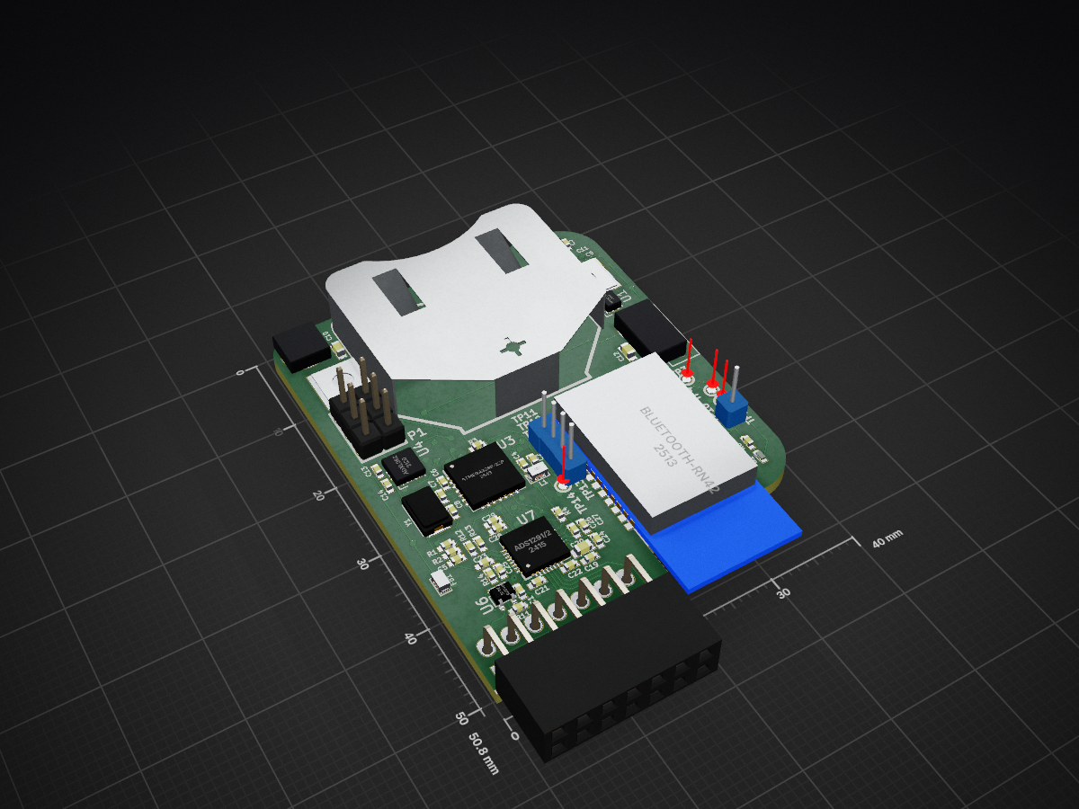
4 layers40 × 50.8 mmEeg brainboard wearable, the printed circuit board in 3D

Eeg brainboard wearable

PCBench/PCBench21

resolution = [0.5, 0.5] pcbfolder = '../PCBs/' pcbnames = ["1Bitsy1bitsy"] iters = 30 env = PCBRoutingEnv(resolution=resolution, pcbfolder=pcbfolder, pcbnames=pcbnames) obs, info = env.reset() for in range(iters): act =…

Size
40 × 50.8 mm
Copper layers
4
Thickness
1.6 mm
Parts
59
Nets
48
Pads
246
Tracks, vias
802, 54
Routed
Yes
KiCad
KiCad 5 (file 20171130)
Created
28 Mar 2023
Updated
18 Jan 2024

Overview

Eeg brainboard wearable is an open-source printed circuit board by PCBench, from the PCBench/PCBench repository on GitHub, published under the MIT licence. It is a 4-layer board of 40 × 50.8 mm with 59 parts on 48 nets, routed with 802 tracks and 54 vias.

It is built around the OPA376AID, FR015L3EZ and ABM3B-8.000MHZ-B2-T, with the BLM18PG121SN1 and JS102011SAQN among its other parts. Its parts include 25 capacitors, 9 resistors, 7 ICs, 2 connectors and 1 diode. It belongs with the wearables boards and the AVR (ATmega, ATtiny) boards of this library.

Main components

5

README

README.md

PCBench: A Dataset for Printed Circuit Board Routing

PCBench is a dataset for PCB routing task, it includes a dataset consisting of 164 printed circuit boards (PCB), a data augmentation script to expand the dataset for supervised learning (SL) tasks, and a reinforcement learning (RL) environment.

Dataset

Folder Structure

All the PCB designs in our dataset are stored in the folder PCBs, where each PCB design is stored in a subfolder named {author/org}_{PCB_name}_{design_version(optional)}. Below is the folder structure of the dataset.

text
├── PCBs
│   ├── master_metadata.json
│   ├── subfolder1
│   │   ├── raw.kicad_pcb
│   │   ├── processed.kicad_pcb
│   │   ├── final.json
│   │   ├── metadata.json
│   │   ├── visual.png
│   ├── subfolder2
│   │   ├── raw.kicad_pcb
│   │   ├── processed.kicad_pcb
│   │   ├── final.json
│   │   ├── metadata.json
│   │   ├── visual.png
│   ├── ...

The raw.kicad_pcb is the raw PCB design file, process.kicad_pcb is the file after cleaning up, final.json stores only routing-related information used for ML tasks. metadata.json stores the meta information for each single PCB design. visual.png is a visualization of each single PCB design. master_meta.json contains metadata of all PCBs and global-level information.

PCB Routing Description Language (PCB-RDL)

We propose a JSON specification (final.json for each PCB design) called the PCB Routing Description Language (PCB-RDL) that expresses a PCB routing problem and its solutions intuitively using basic concepts in order to facilitate research into automated PCB routing using ML. Following figure shows is an example of PCB with marked components in PCB-RDL (Left) and it corrsponding PCB-RDL (Right).

PCB example

Data Augmentation

Run

The augmentation data can be generated with the script Scripts/Data_augmentation/augmentation.py. To generate 3 samples by randomly extracting 50% nets from the PCB 1Bitsy_1bitsy, please run the following command

text
cd Scripts/Data_augmentation/
python augmentation.py --num_samples 3 --net_ratio 0.5 --pcb_name 1Bitsy_1bitsy

Output

All the generated PCBs will be stored in the folder named augmented_data under Scripts/Data_augmentation/. In augmented_data, all the generated samples will be stored in a subfolder with the name of selected PCB. Each generated sample has the name sample_index.json. For example, the above command will generate the following file under Scripts/Data_augmentation/

text
├── augmented_data
│   ├── 1Bitsy_1bitsy
│   │   ├── 1.json
│   │   ├── 2.json
│   │   ├── 3.json

RL environment

Installation

The RL environment requires Python >= 3.7. You can simply install the environment with the following commands:

text
git clone https://github.com/PCBench/PCBench.git
cd PCBench
python setup.py install

After installation, open a Python console and type

text
from RLEnv.EnvLayer.PCBRoutingEnv import PCBRoutingEnv

If no error occurs, you have successfully installed the PCB routing environment.

API Usage

The following content shows an example of API usage of PCBRoutingEnv.

text
from RLEnv.EnvLayer.PCBRoutingEnv import PCBRoutingEnv
import random

resolution = [0.5, 0.5]
pcb_folder = '../PCBs/'
pcb_names = ["1Bitsy_1bitsy"]
iters = 30
env = PCBRoutingEnv(resolution=resolution, pcb_folder=pcb_folder, pcb_names=pcb_names)
obs, info = env.reset()
for _ in range(iters):
    act = random.randint(0,5)
    obs, rew, terminal, _, info = env.step(act)
    if terminal:
        env.reset()

You can find more examples of customizing functions of reward and state observation from RLEnv/examples.ipynb.

Parts

59
QtyValueFootprintReferences
100.1uFc_0402C1, C2, C4, C5, C6, C13, C14, C19, C27, C29
61uFc_0402C3, C11, C23, C24, C26, C28
410kr_0402R3, R4, R12, R13
410uFc_0603C9, C10, C12, C20
21Mr_0402R2, R14
230pFc_0402C7, C8
24.7nFc_0402C21, C22
11.5nFc_0402C25
110uHinductor_smd_0603L1
12.2Mr_0402R1
12.2kr_0402R6
13V3testpoint_1mmTP4
151kr_0402R11
1ABM3B-8.000MHZcrystal_smd_5x3.2mmY1
1ADS1291/2s-pvqfn-n32-nopadU7
1ADXL36216-LGA-3x3.25U4
1ATMEGA328P-28PINqfn-28-nopadU3
1BLM18PG121SN1inductor_smd_0603FB1
1BLUETOOTH-RN42w_rf_modules:roving_rn-42U5
1BTCTSPINTSTTP13
1BTRTSPINTSTTP12
1BTRXPINTSTTP10
1BTTXPINTSTTP11
1CONNtestpoint_1mmTP14
1CONN_7X2pin_socket_7x2-90P2
1FACTtestpoint_1mmTP16
1FR015L3EZMLP6-2x2U1
1GNDtestpoint_1mmTP3
1ICSPpin_strip_3x2P1
1JS102011SAQNJS102011SAQNS1
1LIR2450keystone_3008BT1
1MHOLEmounting_hole_0in125MTG1
1OPA376sc70-5U6
1REDLed_0402D1
1STATUSPINTSTTP17
1TPS727XXDSES-PWSON-N6U2

Questions

How big is the Eeg brainboard wearable PCB?

It measures 40 × 50.8 mm and has 4 copper layers, 1.6 mm thick.

What parts does the Eeg brainboard wearable use?

59 parts, built around the OPA376AID, FR015L3EZ, ABM3B-8.000MHZ-B2-T and BLM18PG121SN1. The full list of its parts is on this page, with links to each part's symbol and footprint where PCBKit's library has them.

Where can I download the Eeg brainboard wearable KiCad files?

From the PCBench/PCBench repository on GitHub, at the commit this page was made from: the board is PCBs/eeg_brainboard_wearable/processed.kicad_pcb. PCBKit opens the board in the browser, with nothing to install.

Can I use the Eeg brainboard wearable design in my own project?

Its repository publishes it under the MIT licence: you may reuse it on that licence's terms (keep the author's notice, and for a copyleft licence share your changes alike).

More from PCBench/PCBench

12
  • 2 layers398.2 × 398.2 mmLargeWordClock LargeKickstarter, the printed circuit board in 3D

    LargeWordClock LargeKickstarter

    PCBench/PCBench

    resolution = [0.5, 0.5] pcbfolder = '../PCBs/' pcbnames = ["1Bitsy1bitsy"] iters = 30 env = PCBRoutingEnv(resolution=resolution, pcbfolder=pcbfolder, pcbnames=pcbnames) obs, info = env.reset() for in range(iters): act =…

    1,591 parts21MIT
  • 4 layers95 × 95 mmRaw, the printed circuit board in 3D

    Raw

    PCBench/PCBench

    resolution = [0.5, 0.5] pcbfolder = '../PCBs/' pcbnames = ["1Bitsy1bitsy"] iters = 30 env = PCBRoutingEnv(resolution=resolution, pcbfolder=pcbfolder, pcbnames=pcbnames) obs, info = env.reset() for in range(iters): act =…

    455 parts21MIT
  • 2 layers90 × 90 mmMod12003 mod12003, the printed circuit board in 3D

    Mod12003 mod12003

    PCBench/PCBench

    resolution = [0.5, 0.5] pcbfolder = '../PCBs/' pcbnames = ["1Bitsy1bitsy"] iters = 30 env = PCBRoutingEnv(resolution=resolution, pcbfolder=pcbfolder, pcbnames=pcbnames) obs, info = env.reset() for in range(iters): act =…

    452 parts21MIT
  • 2 layers88.9 × 114.3 mmRaw, the printed circuit board in 3D

    Raw

    PCBench/PCBench

    resolution = [0.5, 0.5] pcbfolder = '../PCBs/' pcbnames = ["1Bitsy1bitsy"] iters = 30 env = PCBRoutingEnv(resolution=resolution, pcbfolder=pcbfolder, pcbnames=pcbnames) obs, info = env.reset() for in range(iters): act =…

    190 parts21MIT
  • 2 layers100 × 100 mmMod1base mod1base, the printed circuit board in 3D

    Mod1base mod1base

    PCBench/PCBench

    resolution = [0.5, 0.5] pcbfolder = '../PCBs/' pcbnames = ["1Bitsy1bitsy"] iters = 30 env = PCBRoutingEnv(resolution=resolution, pcbfolder=pcbfolder, pcbnames=pcbnames) obs, info = env.reset() for in range(iters): act =…

    187 parts21MIT
  • 6 layers117 × 55 mmKiwiSDR PCB kiwi, the printed circuit board in 3D

    KiwiSDR PCB kiwi

    PCBench/PCBench

    resolution = [0.5, 0.5] pcbfolder = '../PCBs/' pcbnames = ["1Bitsy1bitsy"] iters = 30 env = PCBRoutingEnv(resolution=resolution, pcbfolder=pcbfolder, pcbnames=pcbnames) obs, info = env.reset() for in range(iters): act =…

    173 parts21MIT
  • 4 layers143 × 74 mmKitspace lpa96, the printed circuit board in 3D

    Kitspace lpa96

    PCBench/PCBench

    resolution = [0.5, 0.5] pcbfolder = '../PCBs/' pcbnames = ["1Bitsy1bitsy"] iters = 30 env = PCBRoutingEnv(resolution=resolution, pcbfolder=pcbfolder, pcbnames=pcbnames) obs, info = env.reset() for in range(iters): act =…

    161 parts21MIT
  • 2 layers101.6 × 99.7 mmRaw, the printed circuit board in 3D

    Raw

    PCBench/PCBench

    resolution = [0.5, 0.5] pcbfolder = '../PCBs/' pcbnames = ["1Bitsy1bitsy"] iters = 30 env = PCBRoutingEnv(resolution=resolution, pcbfolder=pcbfolder, pcbnames=pcbnames) obs, info = env.reset() for in range(iters): act =…

    158 parts21MIT
  • 4 layers36.1 × 32.7 mmKitspace tri panel 4up r0.1, the printed circuit board in 3D

    Kitspace tri panel 4up r0.1

    PCBench/PCBench

    resolution = [0.5, 0.5] pcbfolder = '../PCBs/' pcbnames = ["1Bitsy1bitsy"] iters = 30 env = PCBRoutingEnv(resolution=resolution, pcbfolder=pcbfolder, pcbnames=pcbnames) obs, info = env.reset() for in range(iters): act =…

    157 parts21MIT
  • 2 layers101.6 × 99.7 mmKarabas nano karabas nano revB, the printed circuit board in 3D

    Karabas nano karabas nano revB

    PCBench/PCBench

    resolution = [0.5, 0.5] pcbfolder = '../PCBs/' pcbnames = ["1Bitsy1bitsy"] iters = 30 env = PCBRoutingEnv(resolution=resolution, pcbfolder=pcbfolder, pcbnames=pcbnames) obs, info = env.reset() for in range(iters): act =…

    147 parts21MIT
  • 4 layers65 × 60 mmReworkctf reworkctf, the printed circuit board in 3D

    Reworkctf reworkctf

    PCBench/PCBench

    resolution = [0.5, 0.5] pcbfolder = '../PCBs/' pcbnames = ["1Bitsy1bitsy"] iters = 30 env = PCBRoutingEnv(resolution=resolution, pcbfolder=pcbfolder, pcbnames=pcbnames) obs, info = env.reset() for in range(iters): act =…

    143 parts21MIT
  • 2 layers99.1 × 99.1 mmRaw, the printed circuit board in 3D

    Raw

    PCBench/PCBench

    resolution = [0.5, 0.5] pcbfolder = '../PCBs/' pcbnames = ["1Bitsy1bitsy"] iters = 30 env = PCBRoutingEnv(resolution=resolution, pcbfolder=pcbfolder, pcbnames=pcbnames) obs, info = env.reset() for in range(iters): act =…

    77 parts21MIT

Similar boards

  • 2 layersBrainboard wearable, the printed circuit board in 3D

    Brainboard wearable

    gskelly/eeg

    Software, firmware, and CAD files for mobile EEG project.

    30 parts21
  • 2 layers58.5 × 25 mmCurrent sensor, the printed circuit board in 3D

    Current sensor

    paltatech/current_sensor

    Isolated delta sigma current sensor for high speed high current application

    47 parts8
  • 2 layers50 × 20 mmOpamp path, the printed circuit board in 3D

    Opamp path

    afkiwers/GroundTruth

    KiCad 10 plugin and CLI that simulates return currents, EMI, power stages, PDN impedance and thermal rise with a field solver, and suggests vias and design fixes.
    4 partsGPL-3.0
  • 4 layers100 × 123 mmDuet2, the printed circuit board in 3D

    Duet2

    Duet3D/Duet-2-Hardware

    The KiCAD source for the Duet 3d printer controller see www.duet3d.com

    356 parts258
  • 4 layers241.7 × 56.7 mmDaisy studio, the printed circuit board in 3D

    Daisy studio

    squeedee/daisy-studio

    Daisy Seed Carrier for Balanced Pro Audio

    141 parts14MIT
  • 2 layers50 × 110 mmOgham merged v1.0, the printed circuit board in 3D

    Ogham merged v1.0

    keeos-io/ogham

    Ogham — a dual-voice bytebeat synthesizer for Eurorack. Firmware (MIT) and hardware (CC BY-SA 4.0).

    109 parts3
  • 6 layers49.6 × 103 mmAnalogue board pico revb routed, the printed circuit board in 3D

    Analogue board pico revb routed

    Eight4aWish/eurorack_electronics

    Analogue designs and breadboard layouts: the Dual Pingable LPG, and the board behind Boy.

    361 parts1