2 layers

 squeedee/daisy-studio14
Daisy Seed Carrier for Balanced Pro Audio
Daisy studio is an open-source printed circuit board by squeedee, from the squeedee/daisy-studio repository on GitHub, published under the MIT licence. It is a 4-layer board of 241.7 × 56.7 mm with 141 parts on 108 nets, routed with 1,333 tracks and 2,685 vias.
It is built around the RS3-1212D, OPA1656ID and H11L1, with the LM2903, TPS54302 and SM4004 among its other parts. Its parts include 44 capacitors, 38 resistors, 13 diodes, 13 connectors and 10 ICs.


| Front | Back |
|---|---|
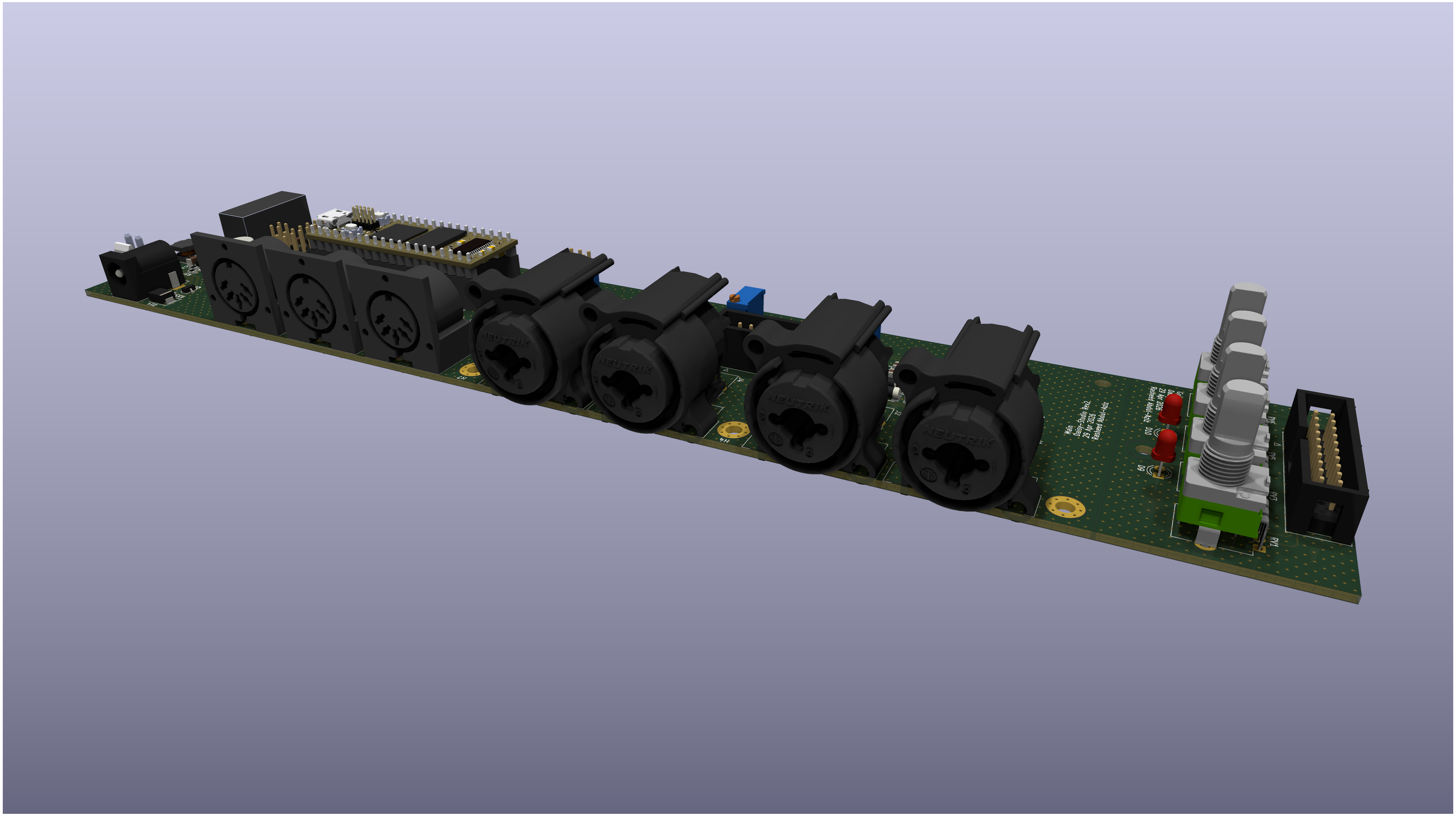 | 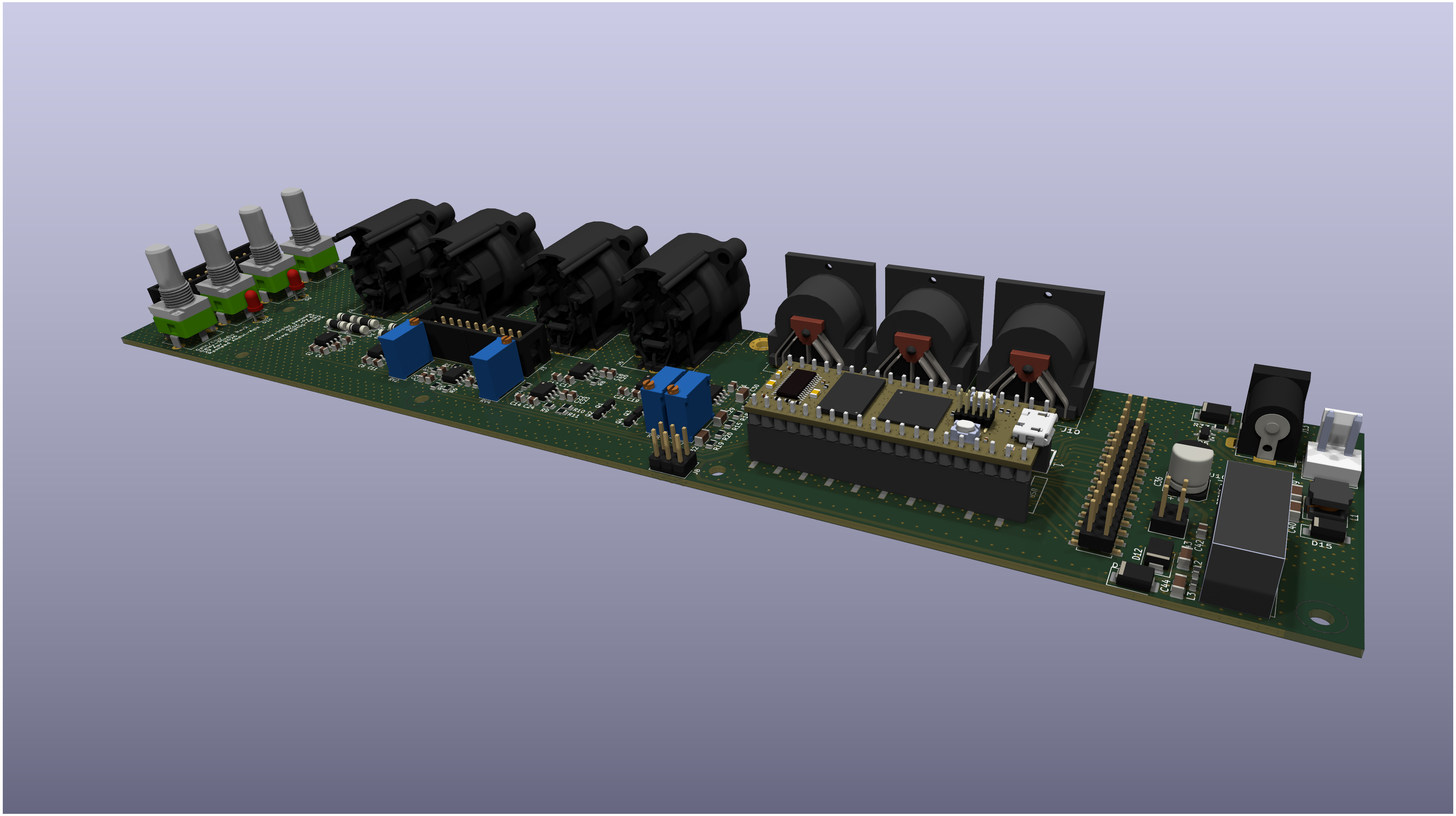 |
A development board for the Electrosmith Daisy Seed DSP module, providing professional studio-grade balanced line input and output.
Schematic PDF: docs/Daisy Studio Rev2.pdf
THD measurement report (Board 1, loopback, post-F9 retrim — ≤ −88 dB / ≤ 0.004 % @ 1 kHz): docs/Daisy THD Meter.pdf
The board is designed as a flexible development board to prototype designs for:
The main PCB carries all active circuitry and connects to a passive daughterboard that holds the user-facing controls (level pots, clip LEDs).
The designer can replace the daughterboard with controls connected however they desire.
Balanced in → THAT1246 → OPA1656 (fixed gain) → daughterboard pot
                                                       ↓
   Daisy Seed ← C_aa anti-alias ← BJT clamp ← R_out (3.3 kΩ) ←
The THAT1246 balanced receiver converts the differential XLR input
to single-ended at −6 dB, keeping +24 dBu peaks within the ±10 V output
swing of the ±12 V rails. Its Sense pin (5) is brought back as a
separate trace to the OPA1656 inverting node — Kelvin-connected past
the input resistor — so the THAT1246's internal feedback amp absorbs
any voltage drop across R_in, eliminating it as a gain-error term.
The OPA1656 runs as an inverting amplifier at a fixed gain of 1.2× (R_fb = 12 kΩ, R_in = 10 kΩ). At +24 dBu peak input the op-amp output reaches ±10.45 V, ~550 mV from the ±11 V clip rails. Fixed gain (rather than a pot in the feedback path) keeps loop phase margin constant across user level adjustments, and the high-impedance summing junction stays entirely on the main PCB.
User level is set by a 10 kΩ log pot on the daughterboard, wired
as a passive three-terminal voltage divider downstream of the op-amp.
Both header legs are low-impedance: the op-amp drives the CW terminal,
and the pot wiper returns to the main PCB into R_out (3.3 kΩ) which
caps fault current into the clamp under pathological overdrive.
The BJT clamp is the design's centrepiece. A complementary pair (2N3906 PNP + 2N3904 NPN) per channel clamps the Seed input pin against ±1.565 V references derived from the ±12 V rails by 10 kΩ / 1.5 kΩ dividers and held stiff at audio frequencies by 47 µF MLCCs. The transistors' β ≈ 200 means only Ic / β flows through the reference divider base connection, so the references stay nearly stationary even under sustained overdrive — the "reference pumping" failure mode that limits passive diode clamps. The sharp emitter-base knee (NF ≈ 1.24, versus ~1.82 for diodes) lets the clean signal use the full ADC range with no distortion. Simulations across five tolerance corners shows worst-case codec voltage of 4.64 V under +24 dBu pathological overdrive — 164 mV margin to the PCM3060's 4.8 V damage ceiling.
A 1 nF C0G capacitor at the Seed input pin, after the clamp, forms
a single-pole LPF with R_out plus the pot wiper source impedance.
The corner stays between 27 kHz (pot mid) and 48 kHz (pot ends), well
above the audio band, attenuating wideband op-amp noise and out-of-band
content before it reaches the PCM3060's sigma-delta ADC.
A clip indicator uses an LM2903 comparator monitoring the Seed input against an adjustable threshold. A trim pot on the daughterboard (0 V to +1.565 V) sets the threshold; the open-collector output sinks an LED current path against +12 V through a 1 kΩ limit on the main PCB. At audio frequencies the LED flickers faster than the eye sees — a dim glow at light clipping, bright at heavy. A single LM2903 covers both channels.
Standard MIDI 1.0 — a 5 mA current loop at 31.25 kbaud on three SDS-50J DIN-5 jacks (IN, OUT, THRU).
DIN-5 IN ── 220R × 2 ── 1N4148W ── H11L1SM (opto, Schmitt)
                                       ├── 270R pull-up to +3V3D
                                       ├── → MIDI_RX → Seed UART RX
                                       └── 33R × 2 → DIN-5 THRU

Seed UART TX ── MIDI_TX ── 33R + 10R ── DIN-5 OUT
The H11L1SM Schmitt-trigger optocoupler galvanically isolates the input per the MIDI 1.0 electrical spec and presents clean UART edges to the Seed. THRU buffers the same opto output through a second pair of 33 Ω series resistors. OUT is driven directly from the Seed UART TX through a 33 Ω + 10 Ω series pair.
Seed audio → OPA1656 (gain ~9.1×, C_fb LPF) → daughterboard pot
                                                       ↓
        XLR ← SM4004 phantom clamps ← THAT1646 balanced driver ←
The Seed's PCM3060 outputs 2 V p-p at digital full scale (−1 dBu
single-ended, ~+5 dBu differential through the THAT1646 alone). An
OPA1656 inverting gain stage closes the ~20 dB gap to the +24 dBu
studio peak target. R_in is a fixed 2.2 kΩ; R_fb is 15 kΩ fixed in
series with a 10 kΩ multi-turn cermet trimmer (e.g. Bourns
3296W-1-103). Mid-trim lands at gain ~9.1× (+23.7 dBu peak); the
25-turn trim resolves to ~0.5% of R_fb. The fixed floor prevents
accidental hard clipping if the wiper loses contact, and the ceiling
(R_fb ≤ 25 kΩ) stays below the OPA1656's onset of clipping.
A 100 pF C0G across R_fb turns the gain stage into a single-pole LPF with f_c ≈ 80 kHz at nominal trim. The Seed Rev 7's PCM3060 has out-of-band delta-sigma noise that the codec's internal RC alone does not adequately attenuate; the in-feedback-loop LPF handles this without adding any series parts. C0G dielectric is required — X5R/X7R have voltage-coefficient distortion that would intrude into the audio band when the cap is in the feedback path. Sim shows −0.27 dB at 20 kHz, −22 dB at 1 MHz.
User output level is a 10 kΩ log pot per channel on the daughterboard, voltage-divider-wired downstream of the op-amp. Two separate pots (not ganged) let users pick their own taper or matching strategy. The THAT1646's high-Z input means the op-amp sees a constant 10 kΩ load regardless of wiper position.
The THAT1646 balanced driver converts the single-ended pot wiper back to a differential XLR pair. Sense pins close the feedback loop at the XLR connector for cross-coupled output impedance and immunity to load imbalance.
Phantom-power protection: four SM4004 diodes per channel (two per XLR pin) clamp the THAT1646 output to the ±12 V rails. If an XLR is plugged into a phantom-enabled mic preamp, +48 V through the preamp's 6.8 kΩ feed produces ~5 mA per pin into the clamp — well within the SM4004's 1 A rating.
Rail protection (phantom back-feed when the gear is powered off): one SMBJ15CA bidirectional TVS on each ±12 V rail to AGND, placed near the RS3-1212D output. Same part as the input over-voltage TVS for BOM consolidation. Clamps when the rail magnitude exceeds ~16 V.
The main PCB commits to a 2×10 (20-pin) 2.54 mm pitch through-hole footprint for the daughterboard header. Daughterboard PCBs are fully passive, populating only:
No ICs, no power rails, and no high-impedance feedback nodes cross the header — shorting any two daughterboard signals together cannot damage the main PCB. The 18 needed signal pins fit in the 20-pin footprint with two AGND pins at the bottom; AGND is interleaved on every audio pair.
The same footprint supports two build modes:
Pinout (canonical):
| Pin | Signal | Pin | Signal |
|---|---|---|---|
| 1 | AGND | 2 | AGND |
| 3 | IN_OPA_L | 4 | IN_OPA_R |
| 5 | IN_WIPER_L | 6 | IN_WIPER_R |
| 7 | AGND | 8 | AGND |
| 9 | OUT_OPA_L | 10 | OUT_OPA_R |
| 11 | OUT_WIPER_L | 12 | OUT_WIPER_R |
| 13 | AGND | 14 | AGND |
| 15 | CLIP_LED_A_L | 16 | CLIP_LED_A_R |
| 17 | CLIP_LED_K_L | 18 | CLIP_LED_K_R |
| 19 | AGND | 20 | AGND |
The moderate-Z IN_WIPER_* pair and the fast-edge CLIP_LED_K_* pair
(LM2903 open-collector) sit at opposite ends of the header to limit
capacitive crosstalk on a ribbon. User extensions that need active
circuitry use the GPIO breakout header instead.
A 2×14 (28-pin) 2.54 mm vertical pin header brings out every Seed GPIO not committed to the on-board audio (ADC/DAC), MIDI (UART_RX/TX), or USB (D+/D−, VBUS) — plus +5 V, +3V3D, and DGND for downstream circuits. Pin-to-net assignment is slightly illogical, as they were selected to minimise via count and trace crossings between the Seed and the breakout.
Analog ±12 V rails are not on the breakout (or on the daughterboard header); they distribute through the dedicated power header.
12 V barrel jack → SW1 (panel switch / shunt) → DMP3056L (rev-polarity)
                                                       ↓
                                              SMBJ15CA TVS (overvoltage)
                                                       ↓
                                                100 µF bulk → +12V_RAW
                                                       ├─→ TPS54302 → +5V
                                                       └─→ RS3-1212D → ±12V
A 12 V wall-wart feeds a 2.1 mm barrel jack. SW1 — a JST B2P-VH 2-pin THT header in series after the jack — takes either a pre-crimped shunt harness (default, bypasses the switch) or an external panel switch harness (VHR-2N housing, SVH-21T-P1.1 contacts). Placing the switch before reverse-polarity protection means rev-pol and TVS clamping still function during a miswired wall-wart event regardless of switch state.
Reverse polarity is blocked by a DMP3056L-13 P-FET (VGS_max ±20 V, RDS_on ~51 mΩ) — sized for the −12 V on the gate that this configuration imposes when input is correct. An SMBJ15CA bidirectional TVS clamps any over-voltage spike from a misbehaved supply. A 100 µF / 25 V electrolytic provides bulk on +12V_RAW.
The TPS54302 buck (SOT-23-6) generates +5 V from +12V_RAW for the Daisy Seed and the MIDI front-end. Feedback divider 100 kΩ / 13.3 kΩ sets Vout ≈ 5.07 V; inductor L3 = 10 µH (Bourns SRN6045TA). Output caps are 2× 22 µF / 25 V X7R 1206 (5× voltage derating). A dedicated 10 µF / 25 V X7R 1206 input MLCC sits at the VIN pin to handle the buck's pulsed input current at 500 kHz with low loop inductance — the part the TPS54302 datasheet calls for. A defensive SMAJ5.0A TVS clamps +5 V to GND near the Seed.
The Recom RS3-1212D isolated DC/DC (SIP-8, 3 W, regulated ±2%, ±125 mA per rail) generates the ±12 V analog rails. The output passes through 2× BLM18PG121SN1 ferrite beads into the rest of the board.
Power budget (±12 V rails):
| Consumer | +12V mA | −12V mA |
|---|---|---|
| 2× THAT1246 (input receivers) | 16.0 | 16.0 |
| 2× THAT1646 (output drivers) | 18.0 | 18.0 |
| 1× OPA1656 (input gain, dual) | 7.8 | 7.8 |
| 1× OPA1656 (output gain, dual) | 7.8 | 7.8 |
| BJT clamp reference dividers | 2.1 | 2.1 |
| LM2903 quiescent | 0.5 | 0.5 |
| Total | ~52 | ~52 |
≈ 1.25 W output power against the RS3-1212D's 3 W rating — ~2.4× headroom, defensive margin against component tolerance and operating temperature; margin for user consumption on the power header will be validated and provided as a spec (once the boards are tested)
Grounding: AGND and DGND meet near the Seed's pin 20 (AGND) in a two layer connection between AGND and DGND isolated planes.
AGND and CHASSIS meet only at JP1 (a solder jumper on the underside of the board) Users can isolate the chassis ground of the Neutrik connectors by cutting this jumper. Chassis Ground connects to all three mounting holes left, center and right of the Neutrik connectors.
Designed in KiCad 8 with a hierarchical schematic:
daisy-studio.kicad_sch — root sheetaudio_input.kicad_sch — input section (THAT1246, OPA1656, BJT clamp, LM2903)audio_output.kicad_sch — output section (OPA1656, THAT1646, phantom protection)daisy_seed.kicad_sch — Seed module + MIDI front-end + GPIO breakoutpower.kicad_sch — power section (buck + isolated DC/DC + protection)daughter.kicad_sch — passive daughterboard (separate fab)misc.kicad_sch — daughterboard header and mounting parts for the main board.LTspice simulations validating the input-stage clamp / signal path and
the output reconstruction LPF live under sim/input/ and sim/output/.
Rev 2 — fab sent.
| Qty | Value | Footprint | References |
|---|---|---|---|
| 17 | 100n | Capacitor_SMD:C_0805_2012Metric | C1, C2, C5, C10, C13, C14, C17, C19, C20, C23, C25, C26, C31, C35, C37, C42 +1 |
| 8 | 10u | Capacitor_SMD:C_0805_2012Metric | C3, C4, C7, C11, C12, C18, C21, C28 |
| 8 | SM4004 | Diode_SMD:D_MELF | D1, D2, D3, D4, D5, D6, D7, D8 |
| 5 | 47k | Resistor_SMD:R_0805_2012Metric | R25, R26, R27, R28, R32 |
| 5 | MountingHole | MountingHole:MountingHole_3.2mm_M3 | H2, H5, H8, H10, H11 |
| 4 | 1.5k 1% | Resistor_SMD:R_0805_2012Metric | R12, R14, R15, R19 |
| 4 | 10k 1% | Resistor_SMD:R_0805_2012Metric | R13, R17, R18, R20 |
| 4 | 1n | Capacitor_SMD:C_0805_2012Metric | C9, C16, C22, C24 |
| 4 | 22u 25V | Capacitor_SMD:C_1206_3216Metric | C40, C41, C43, C44 |
| 4 | 47u | Capacitor_SMD:C_1206_3216Metric | C27, C29, C30, C32 |
| 4 | NCJ6FA-H-0 | Connector_Audio:Jack_XLR-6.35mm_Neutrik_NCJ6FA-H-0_Horizontal | J1, J2, J4, J6 |
| 3 | 10k | Resistor_SMD:R_0805_2012Metric | R8, R16, R33 |
| 3 | 33R | Resistor_SMD:R_0805_2012Metric | R21, R22, R23 |
| 3 | MountingHole_Pad | MountingHole:MountingHole_3.2mm_M3_Pad_Via | H1, H4, H7 |
| 3 | SDS-50J | daisy-studio:SDS50J | J7, J9, J10 |
| 3 | SMBJ15CA | Diode_SMD:D_SMB | D12, D13, D14 |
| 2 | 100k | Potentiometer_THT:Potentiometer_Bourns_3296W_Vertical | RV7, RV8 |
| 2 | 100p C0G | Capacitor_SMD:C_0805_2012Metric | C8, C15 |
| 2 | 10k | Potentiometer_THT:Potentiometer_Bourns_3296W_Vertical | RV2, RV4 |
| 2 | 12k 1% | Resistor_SMD:R_0805_2012Metric | R4, R9 |
| 2 | 1k | Resistor_SMD:R_0805_2012Metric | R1, R3 |
| 2 | 1n C0G | Capacitor_SMD:C_0603_1608Metric | C33, C34 |
| 2 | 220R | Resistor_SMD:R_0805_2012Metric | R24, R31 |
| 2 | 2k2 1% | Resistor_SMD:R_0805_2012Metric | R5, R6 |
| 2 | 3.3k 1% | Resistor_SMD:R_0805_2012Metric | R10, R11 |
| 2 | 6.8k | Resistor_SMD:R_0805_2012Metric | R2, R7 |
| 2 | BLM18PG121SN1 | Inductor_SMD:L_0603_1608Metric | L2, L3 |
| 2 | MMBT3904 | Package_TO_SOT_SMD:SOT-23 | Q1, Q4 |
| 2 | MMBT3906 | Package_TO_SOT_SMD:SOT-23 | Q2, Q3 |
| 2 | OPA1656ID | Package_SO:SOIC-8_3.9x4.9mm_P1.27mm | U3, U6 |
| 2 | THAT1246 | Package_SO:SOIC-8_3.9x4.9mm_P1.27mm | U4, U5 |
| 2 | THAT1646 | Package_SO:SOIC-8_3.9x4.9mm_P1.27mm | U1, U2 |
| 1 | 100k | Resistor_SMD:R_0805_2012Metric | R34 |
| 1 | 100k 1% | Resistor_SMD:R_0805_2012Metric | R35 |
| 1 | 100u 25V | Capacitor_SMD:CP_Elec_6.3x7.7 | C36 |
| 1 | 10R | Resistor_SMD:R_0805_2012Metric | R29 |
| 1 | 10u 25V | Capacitor_SMD:C_1206_3216Metric | C39 |
| 1 | 10uH | Inductor_SMD:L_Bourns_SRN6045TA | L1 |
| 1 | 13.3K 1% | Resistor_SMD:R_0805_2012Metric | R38 |
| 1 | 13.7k 1% | Resistor_SMD:R_0805_2012Metric | R37 |
| 1 | 1N4148WS | Diode_SMD:D_SOD-323 | D11 |
| 1 | 270R | Resistor_SMD:R_0805_2012Metric | R30 |
| 1 | 49.9R 1% | Resistor_SMD:R_0805_2012Metric | R36 |
| 1 | 75pF | Capacitor_SMD:C_0805_2012Metric | C38 |
| 1 | Barrel_Jack_MountingPin | Connector_BarrelJack:BarrelJack_Horizontal | J13 |
| 1 | Conn_02x02_Odd_Even | Connector_PinHeader_2.54mm:PinHeader_2x02_P2.54mm_Vertical | J12 |
| 1 | Conn_02x03 | Connector_PinHeader_2.54mm:PinHeader_2x03_P2.54mm_Vertical | J8 |
| 1 | Conn_02x10_Odd_Even | Connector_IDC:IDC-Header_2x10_P2.54mm_Vertical | J3 |
| 1 | Conn_02x14_Odd_Even | Connector_PinHeader_2.54mm:PinHeader_2x14_P2.54mm_Vertical_SMD | J11 |
| 1 | DMP3056L-13 | Package_TO_SOT_SMD:SOT-23-3 | Q5 |
| 1 | Daisy_Seed | daisy-studio:DAISY_SEED_SMT | U9 |
| 1 | H11L1 | Package_DIP:SMDIP-6_W7.62mm | U8 |
| 1 | LM2903 | Package_SO:SOIC-8_3.9x4.9mm_P1.27mm | U7 |
| 1 | Micro_SD_Card_Det2 | Connector_Card:microSD_HC_Hirose_DM3BT-DSF-PEJS | J14 |
| 1 | Power | Connector_JST:JST_VH_B2P-VH_1x02_P3.96mm_Vertical | SW1 |
| 1 | RS3-1212D | daisy-studio:TMR1210 | PS1 |
| 1 | SMAJ5.0A | Diode_SMD:D_SMA | D15 |
| 1 | SolderJumper_2_Bridged | Jumper:SolderJumper-2_P1.3mm_Bridged_Pad1.0x1.5mm | JP1 |
| 1 | TPS54302 | Package_TO_SOT_SMD:SOT-23-6 | U10 |
It measures 241.7 × 56.7 mm and has 4 copper layers, 1.6 mm thick.
141 parts, built around the RS3-1212D, OPA1656ID, H11L1 and LM2903. The full list of its parts is on this page, with links to each part's symbol and footprint where PCBKit's library has them.
From the squeedee/daisy-studio repository on GitHub, at the commit this page was made from: the board is main-board/main-board.kicad_pcb and its schematic daughter-board/daughter-board.kicad_sch. PCBKit opens the board in the browser, with nothing to install.
Its repository publishes it under the MIT licence: you may reuse it on that licence's terms (keep the author's notice, and for a copyleft licence share your changes alike).


MarkWestbroek/MusicBrain
A central brain running on teensy or a lighter MCU to process any control signals (MIDI, CV, our own) into the same but adding logic, ADSRs, DCOs, CV matrices etc. to it


willis936/nixie-clock-ice
Hardware and software source for a GPS nixie tube clock with delay correction.

RyanHailey21/neuromorphic-retina-encoder-pcb
Hardware-accelerated neuromorphic vision encoder and closed-loop motor reflex PCB system built around the Raspberry Pi RP2040 and a 16-neuron hardware Leaky Integrate-and-Fire (LIF) analog spiking neural network.


max-verem/stm32_ltc_encoder
STM32 based SMPTE Linear Timecode Generator/Reader, isolated input/output
