Skip to the content
PCBKitNew board
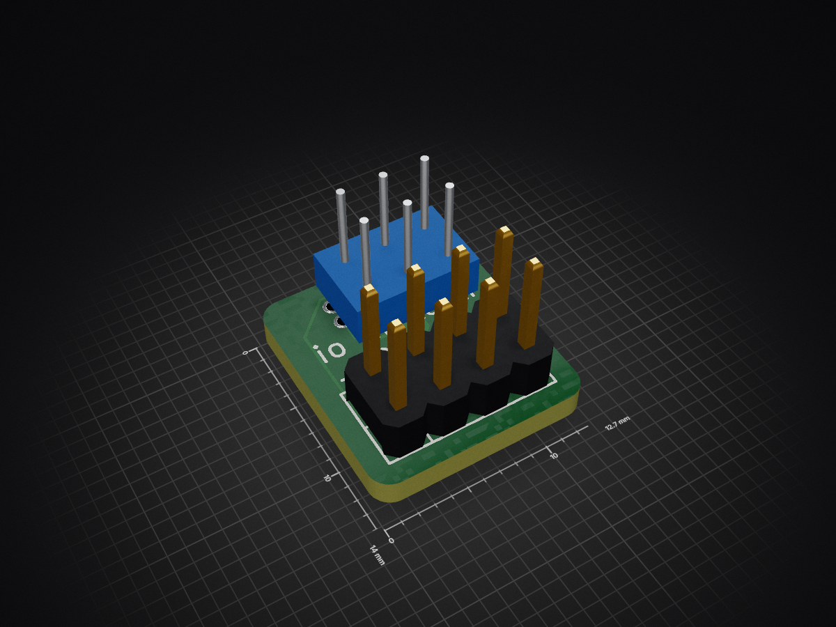
2 layers12.7 × 14 mmBreakout boards swd to wires, the printed circuit board in 3D

Breakout boards swd to wires

PCBench/PCBench21

resolution = [0.5, 0.5] pcbfolder = '../PCBs/' pcbnames = ["1Bitsy1bitsy"] iters = 30 env = PCBRoutingEnv(resolution=resolution, pcbfolder=pcbfolder, pcbnames=pcbnames) obs, info = env.reset() for in range(iters): act =…

Size
12.7 × 14 mm
Copper layers
2
Thickness
1.6 mm
Parts
2
Nets
9
Pads
18
Tracks, vias
56, 1
Routed
Yes
KiCad
KiCad 5 (file 20171130)
Created
28 Mar 2023
Updated
18 Jan 2024

Overview

Breakout boards swd to wires is an open-source printed circuit board by PCBench, from the PCBench/PCBench repository on GitHub, published under the MIT licence. It is a 2-layer board of 12.7 × 14 mm with 2 parts on 9 nets, routed with 56 tracks and 1 via.

It belongs with the interfaces and adapters and microcontroller boards boards of this library.

README

README.md

PCBench: A Dataset for Printed Circuit Board Routing

PCBench is a dataset for PCB routing task, it includes a dataset consisting of 164 printed circuit boards (PCB), a data augmentation script to expand the dataset for supervised learning (SL) tasks, and a reinforcement learning (RL) environment.

Dataset

Folder Structure

All the PCB designs in our dataset are stored in the folder PCBs, where each PCB design is stored in a subfolder named {author/org}_{PCB_name}_{design_version(optional)}. Below is the folder structure of the dataset.

text
├── PCBs
│   ├── master_metadata.json
│   ├── subfolder1
│   │   ├── raw.kicad_pcb
│   │   ├── processed.kicad_pcb
│   │   ├── final.json
│   │   ├── metadata.json
│   │   ├── visual.png
│   ├── subfolder2
│   │   ├── raw.kicad_pcb
│   │   ├── processed.kicad_pcb
│   │   ├── final.json
│   │   ├── metadata.json
│   │   ├── visual.png
│   ├── ...

The raw.kicad_pcb is the raw PCB design file, process.kicad_pcb is the file after cleaning up, final.json stores only routing-related information used for ML tasks. metadata.json stores the meta information for each single PCB design. visual.png is a visualization of each single PCB design. master_meta.json contains metadata of all PCBs and global-level information.

PCB Routing Description Language (PCB-RDL)

We propose a JSON specification (final.json for each PCB design) called the PCB Routing Description Language (PCB-RDL) that expresses a PCB routing problem and its solutions intuitively using basic concepts in order to facilitate research into automated PCB routing using ML. Following figure shows is an example of PCB with marked components in PCB-RDL (Left) and it corrsponding PCB-RDL (Right).

PCB example

Data Augmentation

Run

The augmentation data can be generated with the script Scripts/Data_augmentation/augmentation.py. To generate 3 samples by randomly extracting 50% nets from the PCB 1Bitsy_1bitsy, please run the following command

text
cd Scripts/Data_augmentation/
python augmentation.py --num_samples 3 --net_ratio 0.5 --pcb_name 1Bitsy_1bitsy

Output

All the generated PCBs will be stored in the folder named augmented_data under Scripts/Data_augmentation/. In augmented_data, all the generated samples will be stored in a subfolder with the name of selected PCB. Each generated sample has the name sample_index.json. For example, the above command will generate the following file under Scripts/Data_augmentation/

text
├── augmented_data
│   ├── 1Bitsy_1bitsy
│   │   ├── 1.json
│   │   ├── 2.json
│   │   ├── 3.json

RL environment

Installation

The RL environment requires Python >= 3.7. You can simply install the environment with the following commands:

text
git clone https://github.com/PCBench/PCBench.git
cd PCBench
python setup.py install

After installation, open a Python console and type

text
from RLEnv.EnvLayer.PCBRoutingEnv import PCBRoutingEnv

If no error occurs, you have successfully installed the PCB routing environment.

API Usage

The following content shows an example of API usage of PCBRoutingEnv.

text
from RLEnv.EnvLayer.PCBRoutingEnv import PCBRoutingEnv
import random

resolution = [0.5, 0.5]
pcb_folder = '../PCBs/'
pcb_names = ["1Bitsy_1bitsy"]
iters = 30
env = PCBRoutingEnv(resolution=resolution, pcb_folder=pcb_folder, pcb_names=pcb_names)
obs, info = env.reset()
for _ in range(iters):
    act = random.randint(0,5)
    obs, rew, terminal, _, info = env.step(act)
    if terminal:
        env.reset()

You can find more examples of customizing functions of reward and state observation from RLEnv/examples.ipynb.

Parts

2
QtyValueFootprintReferences
1ARM-SWD-HEADERmyelin-kicad:pin_array_5x2_50milCON1
1CONN_02X04Pin_Headers:Pin_Header_Straight_2x04P1

Questions

How big is the Breakout boards swd to wires PCB?

It measures 12.7 × 14 mm and has 2 copper layers, 1.6 mm thick.

What parts does the Breakout boards swd to wires use?

2 parts. The full list of its parts is on this page, with links to each part's symbol and footprint where PCBKit's library has them.

Where can I download the Breakout boards swd to wires KiCad files?

From the PCBench/PCBench repository on GitHub, at the commit this page was made from: the board is PCBs/breakout-boards_swd-to-wires/processed.kicad_pcb. PCBKit opens the board in the browser, with nothing to install.

Can I use the Breakout boards swd to wires design in my own project?

Its repository publishes it under the MIT licence: you may reuse it on that licence's terms (keep the author's notice, and for a copyleft licence share your changes alike).
More from PCBench/PCBench

12
  • 2 layers398.2 × 398.2 mmLargeWordClock LargeKickstarter, the printed circuit board in 3D

    LargeWordClock LargeKickstarter

    PCBench/PCBench

    resolution = [0.5, 0.5] pcbfolder = '../PCBs/' pcbnames = ["1Bitsy1bitsy"] iters = 30 env = PCBRoutingEnv(resolution=resolution, pcbfolder=pcbfolder, pcbnames=pcbnames) obs, info = env.reset() for in range(iters): act =…

    1,591 parts21MIT
  • 4 layers95 × 95 mmRaw, the printed circuit board in 3D

    Raw

    PCBench/PCBench

    resolution = [0.5, 0.5] pcbfolder = '../PCBs/' pcbnames = ["1Bitsy1bitsy"] iters = 30 env = PCBRoutingEnv(resolution=resolution, pcbfolder=pcbfolder, pcbnames=pcbnames) obs, info = env.reset() for in range(iters): act =…

    455 parts21MIT
  • 2 layers90 × 90 mmMod12003 mod12003, the printed circuit board in 3D

    Mod12003 mod12003

    PCBench/PCBench

    resolution = [0.5, 0.5] pcbfolder = '../PCBs/' pcbnames = ["1Bitsy1bitsy"] iters = 30 env = PCBRoutingEnv(resolution=resolution, pcbfolder=pcbfolder, pcbnames=pcbnames) obs, info = env.reset() for in range(iters): act =…

    452 parts21MIT
  • 2 layers88.9 × 114.3 mmRaw, the printed circuit board in 3D

    Raw

    PCBench/PCBench

    resolution = [0.5, 0.5] pcbfolder = '../PCBs/' pcbnames = ["1Bitsy1bitsy"] iters = 30 env = PCBRoutingEnv(resolution=resolution, pcbfolder=pcbfolder, pcbnames=pcbnames) obs, info = env.reset() for in range(iters): act =…

    190 parts21MIT
  • 2 layers100 × 100 mmMod1base mod1base, the printed circuit board in 3D

    Mod1base mod1base

    PCBench/PCBench

    resolution = [0.5, 0.5] pcbfolder = '../PCBs/' pcbnames = ["1Bitsy1bitsy"] iters = 30 env = PCBRoutingEnv(resolution=resolution, pcbfolder=pcbfolder, pcbnames=pcbnames) obs, info = env.reset() for in range(iters): act =…

    187 parts21MIT
  • 6 layers117 × 55 mmKiwiSDR PCB kiwi, the printed circuit board in 3D

    KiwiSDR PCB kiwi

    PCBench/PCBench

    resolution = [0.5, 0.5] pcbfolder = '../PCBs/' pcbnames = ["1Bitsy1bitsy"] iters = 30 env = PCBRoutingEnv(resolution=resolution, pcbfolder=pcbfolder, pcbnames=pcbnames) obs, info = env.reset() for in range(iters): act =…

    173 parts21MIT
  • 4 layers143 × 74 mmKitspace lpa96, the printed circuit board in 3D

    Kitspace lpa96

    PCBench/PCBench

    resolution = [0.5, 0.5] pcbfolder = '../PCBs/' pcbnames = ["1Bitsy1bitsy"] iters = 30 env = PCBRoutingEnv(resolution=resolution, pcbfolder=pcbfolder, pcbnames=pcbnames) obs, info = env.reset() for in range(iters): act =…

    161 parts21MIT
  • 2 layers101.6 × 99.7 mmRaw, the printed circuit board in 3D

    Raw

    PCBench/PCBench

    resolution = [0.5, 0.5] pcbfolder = '../PCBs/' pcbnames = ["1Bitsy1bitsy"] iters = 30 env = PCBRoutingEnv(resolution=resolution, pcbfolder=pcbfolder, pcbnames=pcbnames) obs, info = env.reset() for in range(iters): act =…

    158 parts21MIT
  • 4 layers36.1 × 32.7 mmKitspace tri panel 4up r0.1, the printed circuit board in 3D

    Kitspace tri panel 4up r0.1

    PCBench/PCBench

    resolution = [0.5, 0.5] pcbfolder = '../PCBs/' pcbnames = ["1Bitsy1bitsy"] iters = 30 env = PCBRoutingEnv(resolution=resolution, pcbfolder=pcbfolder, pcbnames=pcbnames) obs, info = env.reset() for in range(iters): act =…

    157 parts21MIT
  • 2 layers101.6 × 99.7 mmKarabas nano karabas nano revB, the printed circuit board in 3D

    Karabas nano karabas nano revB

    PCBench/PCBench

    resolution = [0.5, 0.5] pcbfolder = '../PCBs/' pcbnames = ["1Bitsy1bitsy"] iters = 30 env = PCBRoutingEnv(resolution=resolution, pcbfolder=pcbfolder, pcbnames=pcbnames) obs, info = env.reset() for in range(iters): act =…

    147 parts21MIT
  • 4 layers65 × 60 mmReworkctf reworkctf, the printed circuit board in 3D

    Reworkctf reworkctf

    PCBench/PCBench

    resolution = [0.5, 0.5] pcbfolder = '../PCBs/' pcbnames = ["1Bitsy1bitsy"] iters = 30 env = PCBRoutingEnv(resolution=resolution, pcbfolder=pcbfolder, pcbnames=pcbnames) obs, info = env.reset() for in range(iters): act =…

    143 parts21MIT
  • 2 layers99.1 × 99.1 mmRaw, the printed circuit board in 3D

    Raw

    PCBench/PCBench

    resolution = [0.5, 0.5] pcbfolder = '../PCBs/' pcbnames = ["1Bitsy1bitsy"] iters = 30 env = PCBRoutingEnv(resolution=resolution, pcbfolder=pcbfolder, pcbnames=pcbnames) obs, info = env.reset() for in range(iters): act =…

    77 parts21MIT

Similar boards

  • 2 layers37 × 19 mmPassive rpi hub75-adapter, the printed circuit board in 3D

    Passive rpi hub75-adapter

    hzeller/rpi-rgb-led-matrix

    Controlling up to three chains of 64x64, 32x32, 16x32 or similar RGB LED displays using Raspberry Pi GPIO

    2 parts4.4kGPL-2.0
  • 2 layersDiode template, the printed circuit board in 3D

    Diode template

    adamws/kicad-kbplacer

    KiCad plugin for automatic keyboard's key placement and routing

    2 parts547GPL-3.0
  • 2 layers20.3 × 15.2 mmL0 button, the printed circuit board in 3D

    L0 button

    Luos-io/luos_engine

    Open-source and real-time orchestrator for cyber-physical-systems, to easily design, test and deploy embedded applications and digital twins.

    2 parts546MIT
  • 2 layers35.1 × 46.8 mmSDEX2M2 Breakout Board, the printed circuit board in 3D

    SDEX2M2 Breakout Board

    NVNTLabs/switch2-SDEX2M2

    Micro SD Express to M.2 NVME Adapter for Nintendo Switch 2

    2 parts542GPL-3.0
  • 2 layers59.3 × 36.6 mmExpansionBoardTemplate, the printed circuit board in 3D

    ExpansionBoardTemplate

    BlueSCSI/BlueSCSI-v2

    BlueSCSI v2/Ultra - an open source, open hardware, SCSI emulator using the Pi Pico PR2040 and Pico 2 RP2350

    2 parts459GPL-3.0
  • 2 layersAlpha.9mm.wire, the printed circuit board in 3D

    Alpha.9mm.wire

    ohmtech-rdi/eurorack-blocks

    Software to Hardware Prototyping for Eurorack using C++, Max/Gen~ or Faust

    2 parts410
  • 2 layers26.7 × 64 mmGpu power, the printed circuit board in 3D

    Gpu power

    dennisss/dacha

    Monorepo for awesome tools/projects/libraries

    2 parts397Apache-2.0