Skip to the content
PCBKitNew board
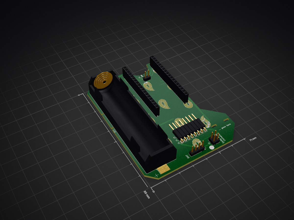
2 layers71 × 89 mmKitspace Heltec Node, the printed circuit board in 3D

Kitspace Heltec Node

PCBench/PCBench21

resolution = [0.5, 0.5] pcbfolder = '../PCBs/' pcbnames = ["1Bitsy1bitsy"] iters = 30 env = PCBRoutingEnv(resolution=resolution, pcbfolder=pcbfolder, pcbnames=pcbnames) obs, info = env.reset() for in range(iters): act =…

Size
71 × 89 mm
Copper layers
2
Thickness
1.6 mm
Parts
35
Nets
35
Pads
75
Tracks, vias
152, 17
Routed
Yes
KiCad
KiCad 5 (file 20171130)
Created
28 Mar 2023
Updated
18 Jan 2024

Overview

Kitspace Heltec Node is an open-source printed circuit board by PCBench, from the PCBench/PCBench repository on GitHub, published under the MIT licence. It is a 2-layer board of 71 × 89 mm with 35 parts on 35 nets, routed with 152 tracks and 17 vias.

README

README.md

PCBench: A Dataset for Printed Circuit Board Routing

PCBench is a dataset for PCB routing task, it includes a dataset consisting of 164 printed circuit boards (PCB), a data augmentation script to expand the dataset for supervised learning (SL) tasks, and a reinforcement learning (RL) environment.

Dataset

Folder Structure

All the PCB designs in our dataset are stored in the folder PCBs, where each PCB design is stored in a subfolder named {author/org}_{PCB_name}_{design_version(optional)}. Below is the folder structure of the dataset.

text
├── PCBs
│   ├── master_metadata.json
│   ├── subfolder1
│   │   ├── raw.kicad_pcb
│   │   ├── processed.kicad_pcb
│   │   ├── final.json
│   │   ├── metadata.json
│   │   ├── visual.png
│   ├── subfolder2
│   │   ├── raw.kicad_pcb
│   │   ├── processed.kicad_pcb
│   │   ├── final.json
│   │   ├── metadata.json
│   │   ├── visual.png
│   ├── ...

The raw.kicad_pcb is the raw PCB design file, process.kicad_pcb is the file after cleaning up, final.json stores only routing-related information used for ML tasks. metadata.json stores the meta information for each single PCB design. visual.png is a visualization of each single PCB design. master_meta.json contains metadata of all PCBs and global-level information.

PCB Routing Description Language (PCB-RDL)

We propose a JSON specification (final.json for each PCB design) called the PCB Routing Description Language (PCB-RDL) that expresses a PCB routing problem and its solutions intuitively using basic concepts in order to facilitate research into automated PCB routing using ML. Following figure shows is an example of PCB with marked components in PCB-RDL (Left) and it corrsponding PCB-RDL (Right).

PCB example

Data Augmentation

Run

The augmentation data can be generated with the script Scripts/Data_augmentation/augmentation.py. To generate 3 samples by randomly extracting 50% nets from the PCB 1Bitsy_1bitsy, please run the following command

text
cd Scripts/Data_augmentation/
python augmentation.py --num_samples 3 --net_ratio 0.5 --pcb_name 1Bitsy_1bitsy

Output

All the generated PCBs will be stored in the folder named augmented_data under Scripts/Data_augmentation/. In augmented_data, all the generated samples will be stored in a subfolder with the name of selected PCB. Each generated sample has the name sample_index.json. For example, the above command will generate the following file under Scripts/Data_augmentation/

text
├── augmented_data
│   ├── 1Bitsy_1bitsy
│   │   ├── 1.json
│   │   ├── 2.json
│   │   ├── 3.json

RL environment

Installation

The RL environment requires Python >= 3.7. You can simply install the environment with the following commands:

text
git clone https://github.com/PCBench/PCBench.git
cd PCBench
python setup.py install

After installation, open a Python console and type

text
from RLEnv.EnvLayer.PCBRoutingEnv import PCBRoutingEnv

If no error occurs, you have successfully installed the PCB routing environment.

API Usage

The following content shows an example of API usage of PCBRoutingEnv.

text
from RLEnv.EnvLayer.PCBRoutingEnv import PCBRoutingEnv
import random

resolution = [0.5, 0.5]
pcb_folder = '../PCBs/'
pcb_names = ["1Bitsy_1bitsy"]
iters = 30
env = PCBRoutingEnv(resolution=resolution, pcb_folder=pcb_folder, pcb_names=pcb_names)
obs, info = env.reset()
for _ in range(iters):
    act = random.randint(0,5)
    obs, rew, terminal, _, info = env.step(act)
    if terminal:
        env.reset()

You can find more examples of customizing functions of reward and state observation from RLEnv/examples.ipynb.

Parts

35
QtyValueFootprintReferences
12LOGOLibs:gl_1G***, G***_4, G***_5, G***_6, G***_7, G***_11, G***_13, G***_15, G***_19, G***_21, G***_23, G***_24
12LOGOLibs:gl_2G***_2, G***_3, G***_8, G***_9, G***_10, G***_12, G***_14, G***_16, G***_17, G***_18, G***_20, G***_22
3Conn_01x08Pin_Headers:Pin_Header_Straight_1x08_Pitch2.54mmJ3, J4, J5
2Conn_01x18_FemaleSocket_Strips:Socket_Strip_Straight_1x18_Pitch2.54mmJ1, J2
1Battery_CellBattery_Holders:Keystone_1042_1x18650BT1
1Conn_01x02Pin_Headers:Pin_Header_Angled_1x02_Pitch2.54mmJ8
1Conn_01x04Pin_Headers:Pin_Header_Straight_1x04_Pitch2.54mmJ7
1Conn_02x02_Top_BottomPin_Headers:Pin_Header_Straight_2x02_Pitch2.54mmJ6

The 33 most common of 35 parts.

Questions

How big is the Kitspace Heltec Node PCB?

It measures 71 × 89 mm and has 2 copper layers, 1.6 mm thick.

What parts does the Kitspace Heltec Node use?

35 parts. The full list of its parts is on this page, with links to each part's symbol and footprint where PCBKit's library has them.

Where can I download the Kitspace Heltec Node KiCad files?

From the PCBench/PCBench repository on GitHub, at the commit this page was made from: the board is PCBs/kitspace_Heltec_Node/processed.kicad_pcb. PCBKit opens the board in the browser, with nothing to install.

Can I use the Kitspace Heltec Node design in my own project?

Its repository publishes it under the MIT licence: you may reuse it on that licence's terms (keep the author's notice, and for a copyleft licence share your changes alike).
More from PCBench/PCBench

12
  • 2 layers398.2 × 398.2 mmLargeWordClock LargeKickstarter, the printed circuit board in 3D

    LargeWordClock LargeKickstarter

    PCBench/PCBench

    resolution = [0.5, 0.5] pcbfolder = '../PCBs/' pcbnames = ["1Bitsy1bitsy"] iters = 30 env = PCBRoutingEnv(resolution=resolution, pcbfolder=pcbfolder, pcbnames=pcbnames) obs, info = env.reset() for in range(iters): act =…

    1,591 parts21MIT
  • 4 layers95 × 95 mmRaw, the printed circuit board in 3D

    Raw

    PCBench/PCBench

    resolution = [0.5, 0.5] pcbfolder = '../PCBs/' pcbnames = ["1Bitsy1bitsy"] iters = 30 env = PCBRoutingEnv(resolution=resolution, pcbfolder=pcbfolder, pcbnames=pcbnames) obs, info = env.reset() for in range(iters): act =…

    455 parts21MIT
  • 2 layers90 × 90 mmMod12003 mod12003, the printed circuit board in 3D

    Mod12003 mod12003

    PCBench/PCBench

    resolution = [0.5, 0.5] pcbfolder = '../PCBs/' pcbnames = ["1Bitsy1bitsy"] iters = 30 env = PCBRoutingEnv(resolution=resolution, pcbfolder=pcbfolder, pcbnames=pcbnames) obs, info = env.reset() for in range(iters): act =…

    452 parts21MIT
  • 2 layers88.9 × 114.3 mmRaw, the printed circuit board in 3D

    Raw

    PCBench/PCBench

    resolution = [0.5, 0.5] pcbfolder = '../PCBs/' pcbnames = ["1Bitsy1bitsy"] iters = 30 env = PCBRoutingEnv(resolution=resolution, pcbfolder=pcbfolder, pcbnames=pcbnames) obs, info = env.reset() for in range(iters): act =…

    190 parts21MIT
  • 2 layers100 × 100 mmMod1base mod1base, the printed circuit board in 3D

    Mod1base mod1base

    PCBench/PCBench

    resolution = [0.5, 0.5] pcbfolder = '../PCBs/' pcbnames = ["1Bitsy1bitsy"] iters = 30 env = PCBRoutingEnv(resolution=resolution, pcbfolder=pcbfolder, pcbnames=pcbnames) obs, info = env.reset() for in range(iters): act =…

    187 parts21MIT
  • 6 layers117 × 55 mmKiwiSDR PCB kiwi, the printed circuit board in 3D

    KiwiSDR PCB kiwi

    PCBench/PCBench

    resolution = [0.5, 0.5] pcbfolder = '../PCBs/' pcbnames = ["1Bitsy1bitsy"] iters = 30 env = PCBRoutingEnv(resolution=resolution, pcbfolder=pcbfolder, pcbnames=pcbnames) obs, info = env.reset() for in range(iters): act =…

    173 parts21MIT
  • 4 layers143 × 74 mmKitspace lpa96, the printed circuit board in 3D

    Kitspace lpa96

    PCBench/PCBench

    resolution = [0.5, 0.5] pcbfolder = '../PCBs/' pcbnames = ["1Bitsy1bitsy"] iters = 30 env = PCBRoutingEnv(resolution=resolution, pcbfolder=pcbfolder, pcbnames=pcbnames) obs, info = env.reset() for in range(iters): act =…

    161 parts21MIT
  • 2 layers101.6 × 99.7 mmRaw, the printed circuit board in 3D

    Raw

    PCBench/PCBench

    resolution = [0.5, 0.5] pcbfolder = '../PCBs/' pcbnames = ["1Bitsy1bitsy"] iters = 30 env = PCBRoutingEnv(resolution=resolution, pcbfolder=pcbfolder, pcbnames=pcbnames) obs, info = env.reset() for in range(iters): act =…

    158 parts21MIT
  • 4 layers36.1 × 32.7 mmKitspace tri panel 4up r0.1, the printed circuit board in 3D

    Kitspace tri panel 4up r0.1

    PCBench/PCBench

    resolution = [0.5, 0.5] pcbfolder = '../PCBs/' pcbnames = ["1Bitsy1bitsy"] iters = 30 env = PCBRoutingEnv(resolution=resolution, pcbfolder=pcbfolder, pcbnames=pcbnames) obs, info = env.reset() for in range(iters): act =…

    157 parts21MIT
  • 2 layers101.6 × 99.7 mmKarabas nano karabas nano revB, the printed circuit board in 3D

    Karabas nano karabas nano revB

    PCBench/PCBench

    resolution = [0.5, 0.5] pcbfolder = '../PCBs/' pcbnames = ["1Bitsy1bitsy"] iters = 30 env = PCBRoutingEnv(resolution=resolution, pcbfolder=pcbfolder, pcbnames=pcbnames) obs, info = env.reset() for in range(iters): act =…

    147 parts21MIT
  • 4 layers65 × 60 mmReworkctf reworkctf, the printed circuit board in 3D

    Reworkctf reworkctf

    PCBench/PCBench

    resolution = [0.5, 0.5] pcbfolder = '../PCBs/' pcbnames = ["1Bitsy1bitsy"] iters = 30 env = PCBRoutingEnv(resolution=resolution, pcbfolder=pcbfolder, pcbnames=pcbnames) obs, info = env.reset() for in range(iters): act =…

    143 parts21MIT
  • 2 layers99.1 × 99.1 mmRaw, the printed circuit board in 3D

    Raw

    PCBench/PCBench

    resolution = [0.5, 0.5] pcbfolder = '../PCBs/' pcbnames = ["1Bitsy1bitsy"] iters = 30 env = PCBRoutingEnv(resolution=resolution, pcbfolder=pcbfolder, pcbnames=pcbnames) obs, info = env.reset() for in range(iters): act =…

    77 parts21MIT

Similar boards

  • 2 layers97.2 × 59.1 mmArmLEDsPrototype, the printed circuit board in 3D

    ArmLEDsPrototype

    hackclub/OnBoard

    💡 Join 1,000 teenagers and make your first PCB with a $100 grant!

    35 parts915
  • 2 layers62 × 42 mmMod cell 0 02, the printed circuit board in 3D

    Mod cell 0 02

    Green-bms/SmartBMS

    Open source Smart Battery Management System

    35 parts756
  • 2 layers75 × 26 mmDIY detector electron variant, the printed circuit board in 3D

    DIY detector electron variant

    ozel/DIY_particle_detector

    A mobile low-cost spectrometer for measuring radioactivity and the energy of ionising radiation like alpha particles and electrons

    35 parts558BSD-2-Clause
  • 2 layers45 × 25 mmReCamera Basically Board, the printed circuit board in 3D

    ReCamera Basically Board

    Seeed-Studio/OSHW-reCamera-Series

    reCamera is a series of open-source AI cameras.

    35 parts495Apache-2.0
  • 2 layers160.8 × 24.4 mmHUD VID RCD PANEL, the printed circuit board in 3D

    HUD VID RCD PANEL

    jrsteensen/OpenHornet

    OpenHornet 1:1 F/A-18C Simulator Repository

    35 parts431
  • 2 layers75 × 50 mmBackplane tester, the printed circuit board in 3D

    Backplane tester

    dennisss/dacha

    Monorepo for awesome tools/projects/libraries

    35 parts397Apache-2.0
  • 2 layers50 × 20.5 mmOtterIron PRO Top, the printed circuit board in 3D

    OtterIron PRO Top

    Jana-Marie/Otter-Iron-PRO

    USB-PD soldering station for JBC C245 handles.

    35 parts321
  • 2 layers50.5 × 67.1 mmHackheld Vega, the printed circuit board in 3D

    Hackheld Vega

    SpacehuhnTech/HackHeld

    Hackable Handheld

    35 parts277