


2 layers70 × 35 mm
 Fescron/Project-LabEmbeddedDesign23
Project-LabEmbeddedDesign2
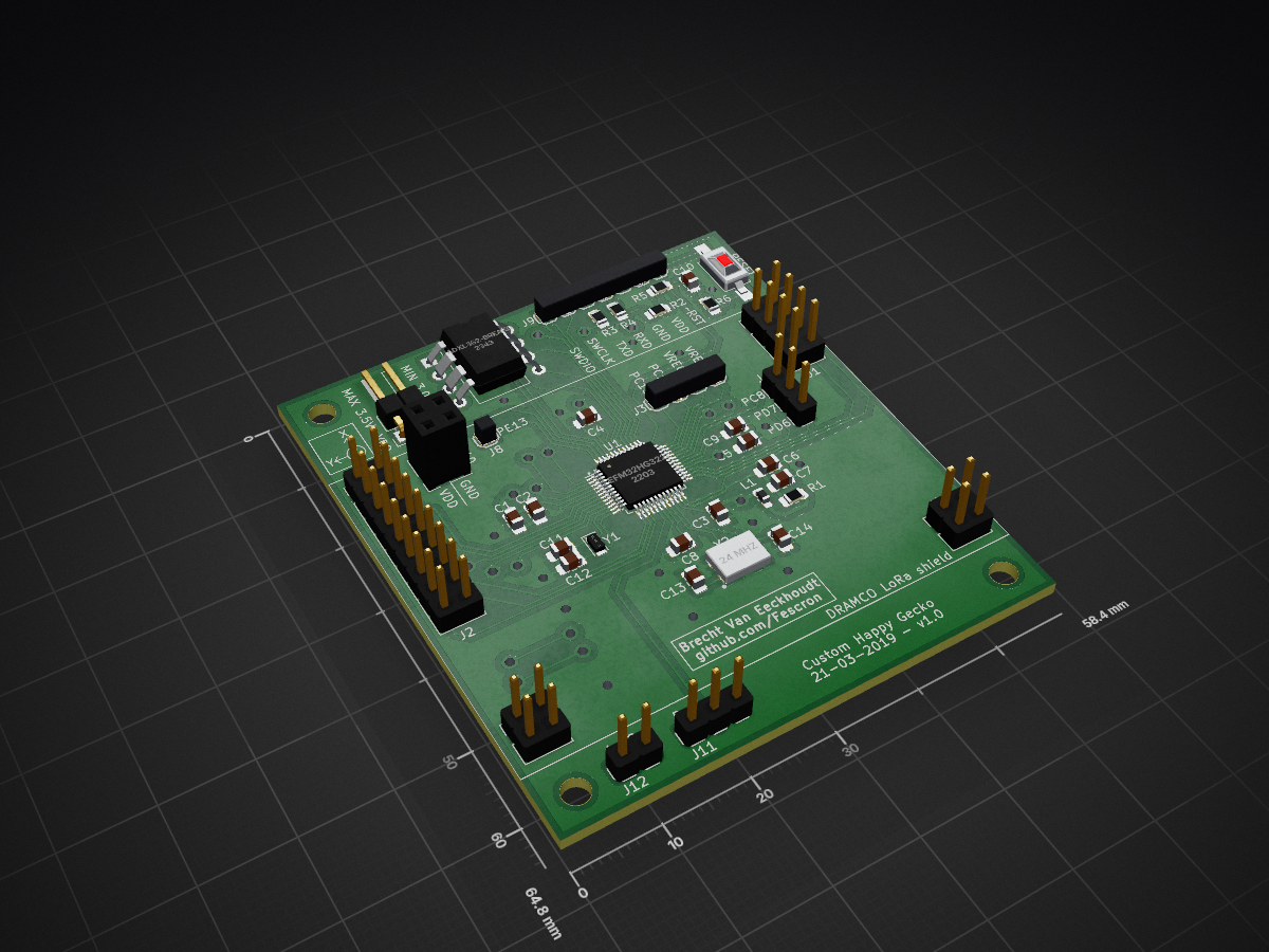
Project embeddedSystemDesign2 is an open-source printed circuit board by Fescron, from the Fescron/Project-LabEmbeddedDesign2 repository on GitHub, published under the GPL-3.0 licence. It is a 2-layer board of 58.4 × 64.8 mm with 41 parts on 46 nets, routed with 397 tracks and 36 vias.
Its parts include 14 capacitors, 12 connectors, 6 resistors, 2 ICs and 2 crystals. It belongs with the radio and wireless and sensors and measurement boards and the Silicon Labs (EFR32, EFM) boards of this library.






This repository contains the presentation, reports and code for the project constructed for Embedded System Design 2 - Lab.
| Location | Content |
|---|---|
| /docs/ | Doxygen code documentation. |
| /documentation/current measurements/ | Documents containing current measurements. |
| /documentation/current measurements/measurements-SF/ | Pictures depicting current profiles for sending 6 measurements at full gain with different LoraWAN Spreading Factors. More information can be found in section "3 - LoRaWAN spreading factor (RN2483)" in this file . |
| /documentation/datasheets/ | General datasheets regarding the used items. |
| /documentation/datasheets/hardware-design/ | Documents regarding hardware design for the EFM32HG microcontroller. |
| /documentation/datasheets/timers-energy-rtc/ | Documents regarding timers, the RTC and energy modes on the EFM32HG microcontroller. |
| /documentation/figures/ | Figures used in reports and the README. |
| /documentation/figures/installation/ | Pictures taken during the project installation. |
| /documentation/reports/ | Reports and presentation. |
| /documentation/schematics/ | Schematics. See this file for the schematic of the self designed PCB and this file for the schematic of the DRAMCO LoRaWAN shield. |
| /hardware/project-embeddedSystemDesign2/ | KiCad PCB design files. See this file for the schematic and this file for the BOM. |
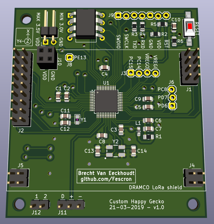
| /hardware/project-embeddedSystemDesign2/3d-renders/ | Pictures of 3D renders of the self designed PCB. On this picture the dimensions are displayed. This is a render of the front and this is a render of the back. |
| /software/EFM32HG-Embedded2-project/ | Code for the project. See this page for general important documentation and this page for information regarding individual files and their methods. This is the decoder for use on The Things Network. |
Note: The code is developed using Simplicity Studio v4 on Ubuntu 18.04 LTS. The code also has dbprint functionality.
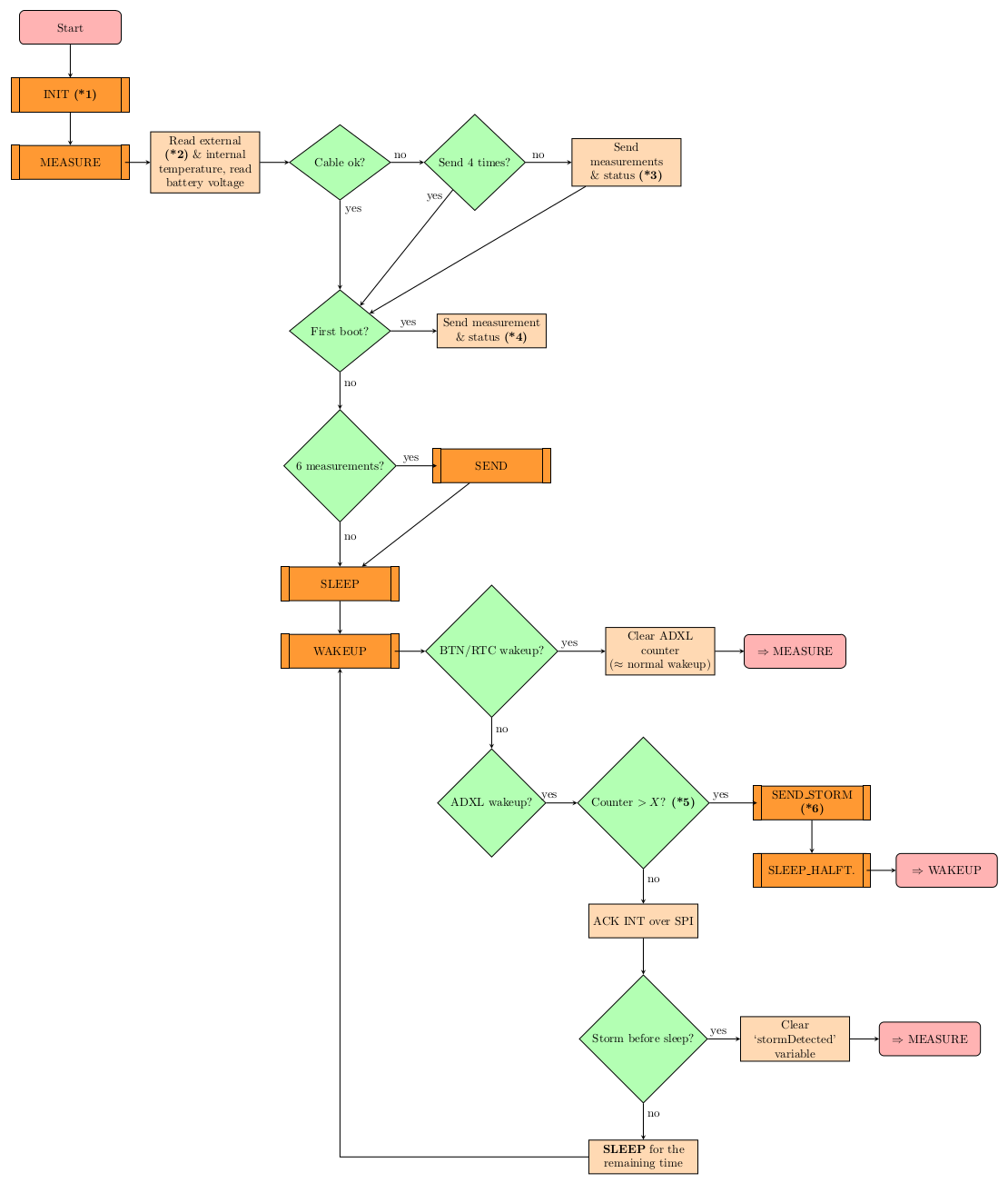
Extra notes on the flowchart:
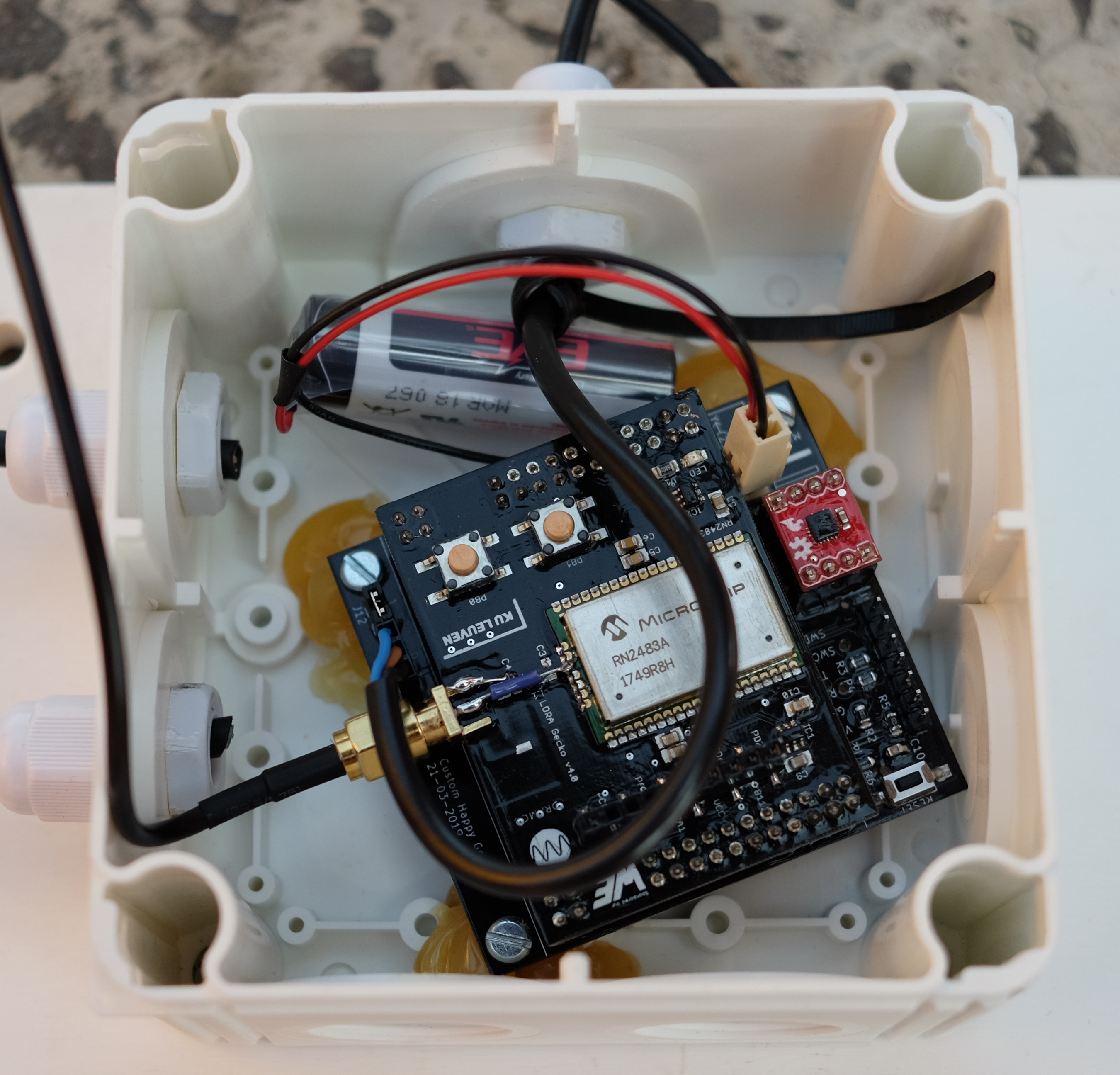
The schematic for the custom PCB misses two resistors. A surface mount 10 kΩ resistor was added between the data and power pin for the DS18B20 temperature sensor. A 3,3 kΩ resistor with wires was added between the BREAK_1pin and VDD. These added resistors can be seen on the bottom right on the left most picture below.
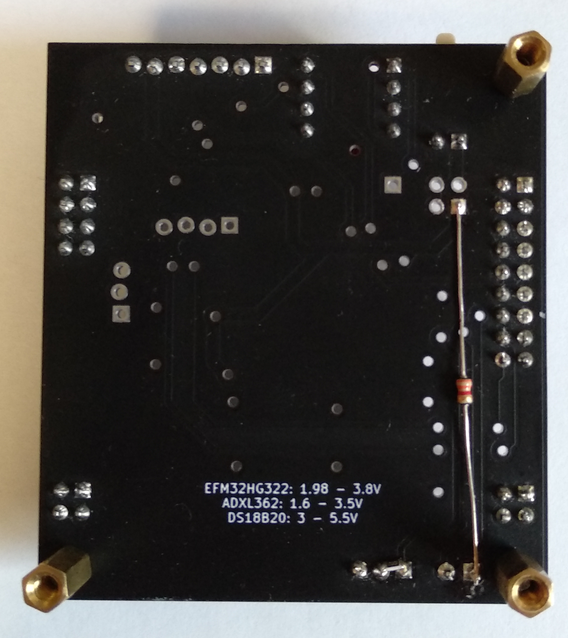
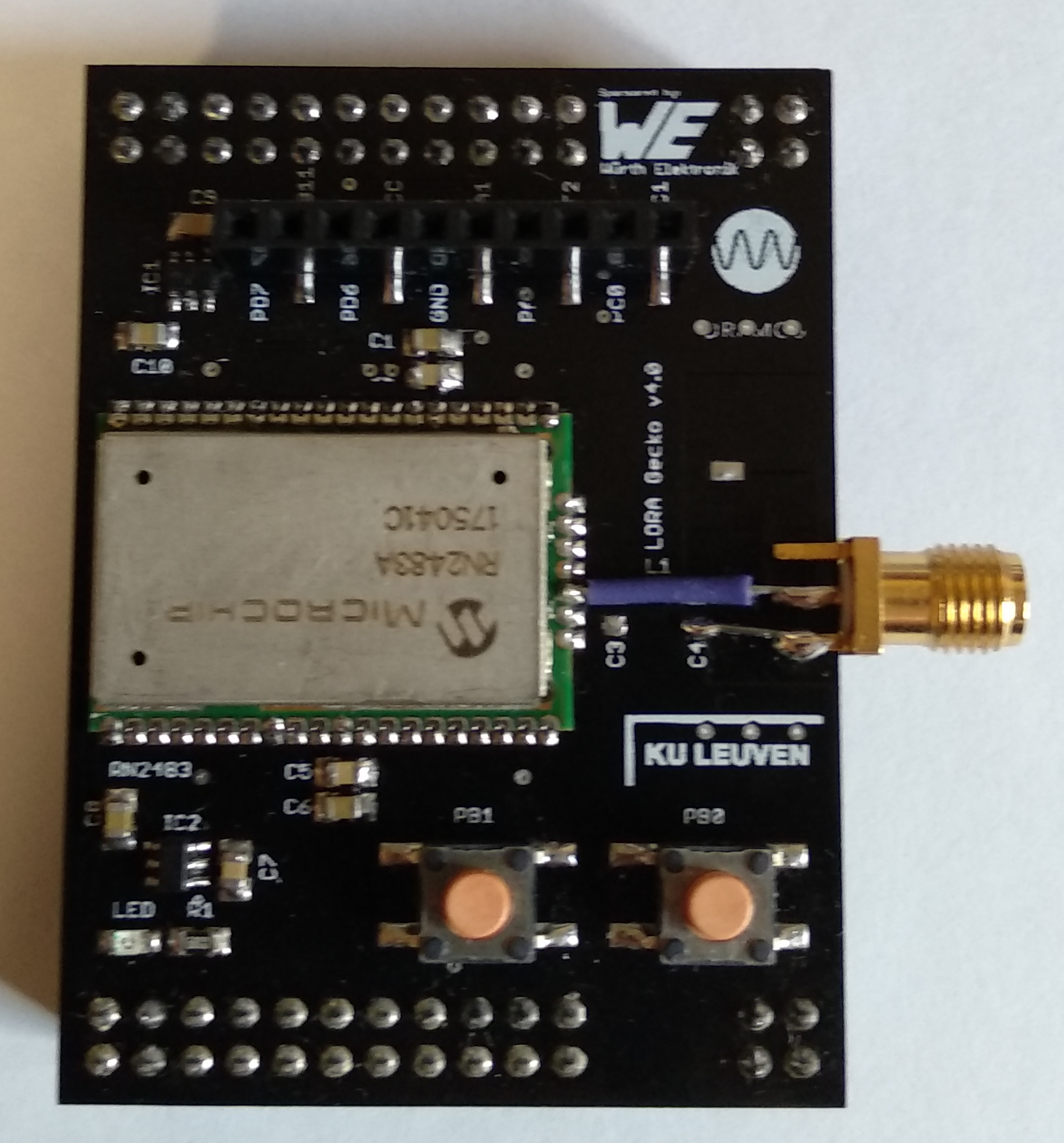
An SMA connector for an external antenna was also added to the DRAMCO LoRaWAN shield. This was done by removing the chip-antenna, capacitors C3 and C4 and inductor L1 and replacing it with an SMA connector directly connected to the signal pin of the RN2483 module. This modification can be seen on the right on the right most picture above.
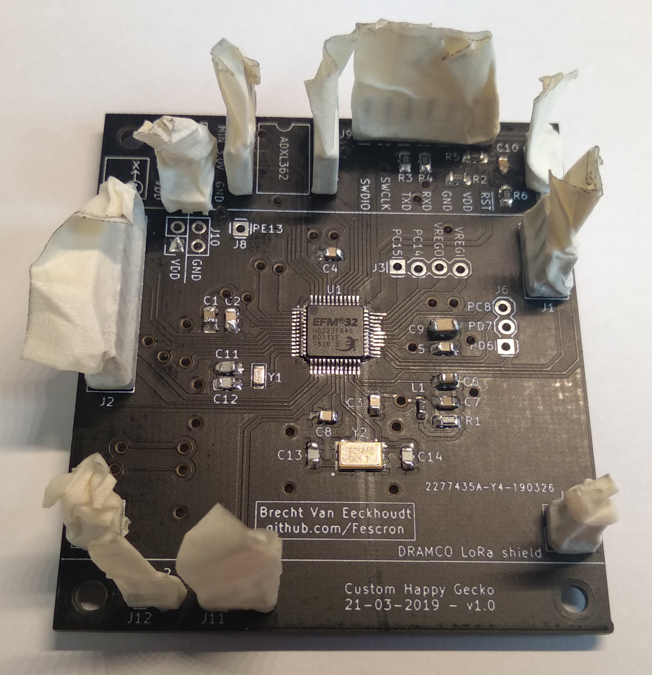
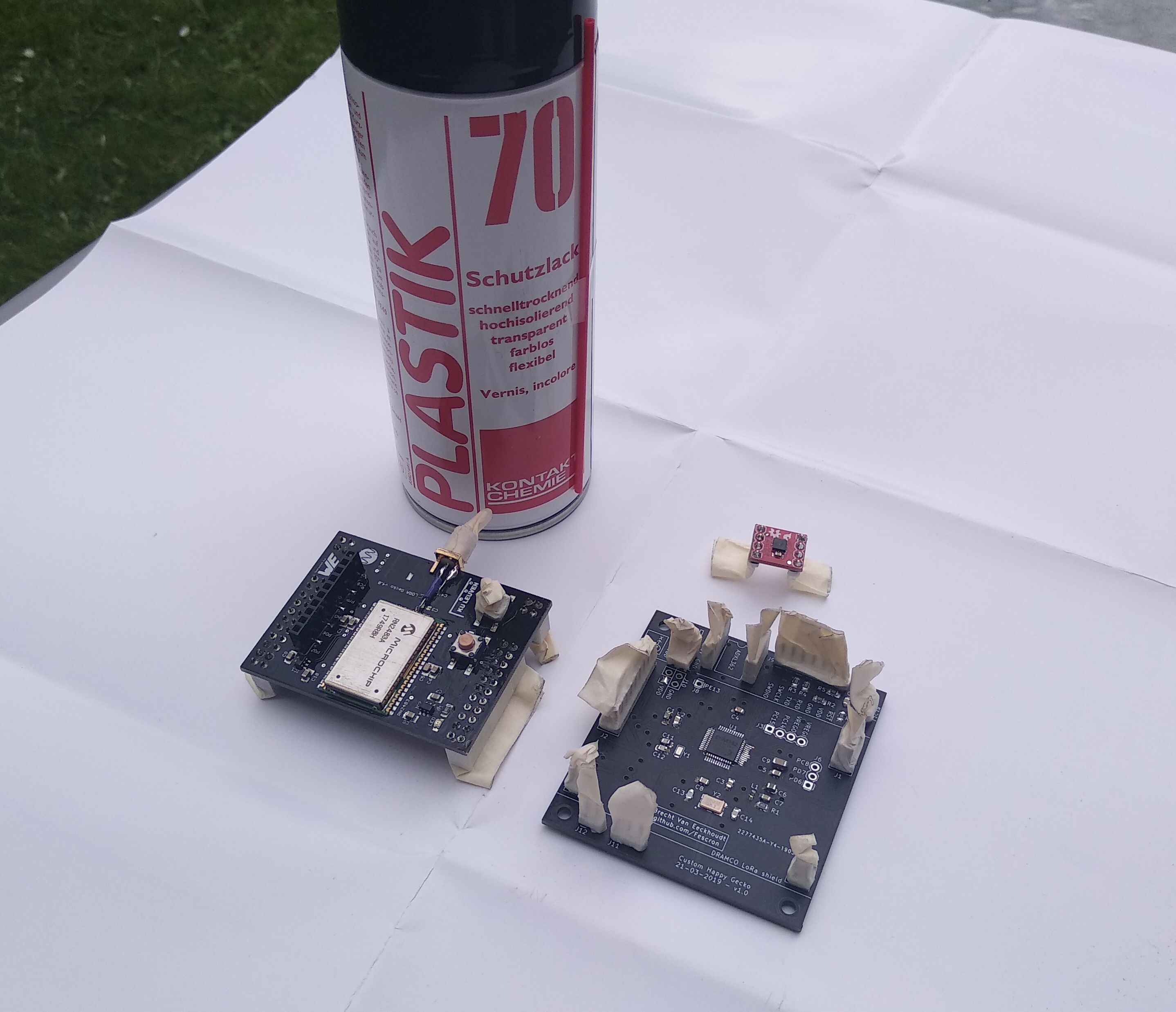
To protect the PCB's from moisture and other contaminants, they were given 2 coats of PLASTIK 70.
| Qty | Value | Footprint | References |
|---|---|---|---|
| 5 | 100 nF | Capacitor_SMD:C_0805_2012Metric_Pad1.15x1.40mm_HandSolder | C2, C3, C4, C5, C10 |
| 3 | 100 Ω | Resistor_SMD:R_0805_2012Metric_Pad1.15x1.40mm_HandSolder | R3, R4, R6 |
| 3 | MountingHole | MountingHole:MountingHole_3mm | H1, H2, H3 |
| 2 | 10 nF | Capacitor_SMD:C_0805_2012Metric_Pad1.15x1.40mm_HandSolder | C7, C8 |
| 2 | 10 µF | Capacitor_SMD:C_0805_2012Metric_Pad1.15x1.40mm_HandSolder | C1, C6 |
| 2 | 12 pF | Capacitor_SMD:C_0805_2012Metric_Pad1.15x1.40mm_HandSolder | C13, C14 |
| 2 | 18 pF | Capacitor_SMD:C_0805_2012Metric_Pad1.15x1.40mm_HandSolder | C11, C12 |
| 2 | Conn_01x03 | Connectors:1X03_LOCK | J6, J11 |
| 2 | Conn_02x02_Odd_Even | Connector_PinHeader_2.54mm:PinHeader_2x02_P2.54mm_Vertical | J4, J5 |
| 1 | 1 kΩ | Resistor_SMD:R_0805_2012Metric_Pad1.15x1.40mm_HandSolder | R5 |
| 1 | 1 µF | Capacitor_SMD:C_0805_2012Metric_Pad1.15x1.40mm_HandSolder | C9 |
| 1 | 1 Ω | Resistor_SMD:R_0805_2012Metric_Pad1.15x1.40mm_HandSolder | R1 |
| 1 | 10 kΩ | Resistor_SMD:R_0805_2012Metric_Pad1.15x1.40mm_HandSolder | R2 |
| 1 | 24 MHz | Clocks:CRYSTAL-SMD-5X3.2-4PAD | Y2 |
| 1 | 32,768 kHz | Crystal:Crystal_SMD_2012-2Pin_2.0x1.2mm_HandSoldering | Y1 |
| 1 | ADXL362-breakout | Package_DIP:DIP-8_W10.16mm | U2 |
| 1 | CBF102WB | Inductor_SMD:L_0603_1608Metric_Pad1.05x0.95mm_HandSolder | L1 |
| 1 | Conn_01x01 | Connectors:1X01 | J8 |
| 1 | Conn_01x02 | Connector_PinHeader_2.54mm:PinHeader_1x02_P2.54mm_Horizontal | J7 |
| 1 | Conn_01x02 | Connectors:1X02_LOCK | J12 |
| 1 | Conn_01x04 | Connectors:1X04_LOCK | J3 |
| 1 | Conn_01x07 | Connectors:1X07_LOCK | J9 |
| 1 | Conn_02x02_Odd_Even | Connector_PinSocket_2.54mm:PinSocket_2x02_P2.54mm_Vertical | J10 |
| 1 | Conn_02x04_Odd_Even | Connector_PinHeader_2.54mm:PinHeader_2x04_P2.54mm_Vertical | J1 |
| 1 | Conn_02x09_Odd_Even | Connector_PinHeader_2.54mm:PinHeader_2x09_P2.54mm_Vertical | J2 |
| 1 | EFM32HG322 | Package_QFP:TQFP-48_7x7mm_P0.5mm | U1 |
| 1 | SW_Push | Button_Switch_SMD:SW_SPST_FSMSM | RESET |
It measures 58.4 × 64.8 mm and has 2 copper layers, 1.6 mm thick.
41 parts. The full list of its parts is on this page, with links to each part's symbol and footprint where PCBKit's library has them.
From the Fescron/Project-LabEmbeddedDesign2 repository on GitHub, at the commit this page was made from: the board is hardware/project-embeddedSystemDesign2/project-embeddedSystemDesign2.kicad_pcb. PCBKit opens the board in the browser, with nothing to install.
Its repository publishes it under the GPL-3.0 licence: you may reuse it on that licence's terms (keep the author's notice, and for a copyleft licence share your changes alike).

VoronDesign/Voron-Hardware
Cool Hardware designed by the Voron Design group

hackclub/OnBoard
💡 Join 1,000 teenagers and make your first PCB with a $100 grant!

openwch/ch32v003
CH32V003 is an ultra-cheap RISC-V MCU with 2KB SRAM, 16KB flash, and up to 18 GPIOs that sells for under $0.10

imchipwood/dumbpad
Simple 4x4 numpad with rotary encoder. Powered by QMK via ATmega32u4 Pro Micro

jrsteensen/OpenHornet
OpenHornet 1:1 F/A-18C Simulator Repository


fabiansteiner/OpenValve
3D-printable pinch valve for irrigation and sensor-driven liquid control.