2 layers99.1 × 99.1 mm
Vent
pandemiaplan/OP-Vent
A Simple, Open-Source Ventilator using a Proportional Solenoid Valve
113 parts5

 UCSIG/attiny85_time_switch1
Low-power time switch using the ATtiny85 microcontroller.
Attiny85 time switch is an open-source printed circuit board by UCSIG, from the UCSIG/attiny85_time_switch repository on GitHub, published under the MIT licence. It is a 2-layer board of 85.7 × 85.7 mm with 32 parts on 19 nets, routed with 157 tracks and 2 vias.
It is built around the ATTINY85V-10PU, FG18X5R1H105KRT06 and BSS84AK,215(ES), with the TL1105AF160Q and PMV20XNER among its other parts. Its parts include 8 connectors, 7 capacitors, 7 resistors, 2 ICs and 2 diodes. It belongs with the AVR (ATmega, ATtiny) boards of this library.


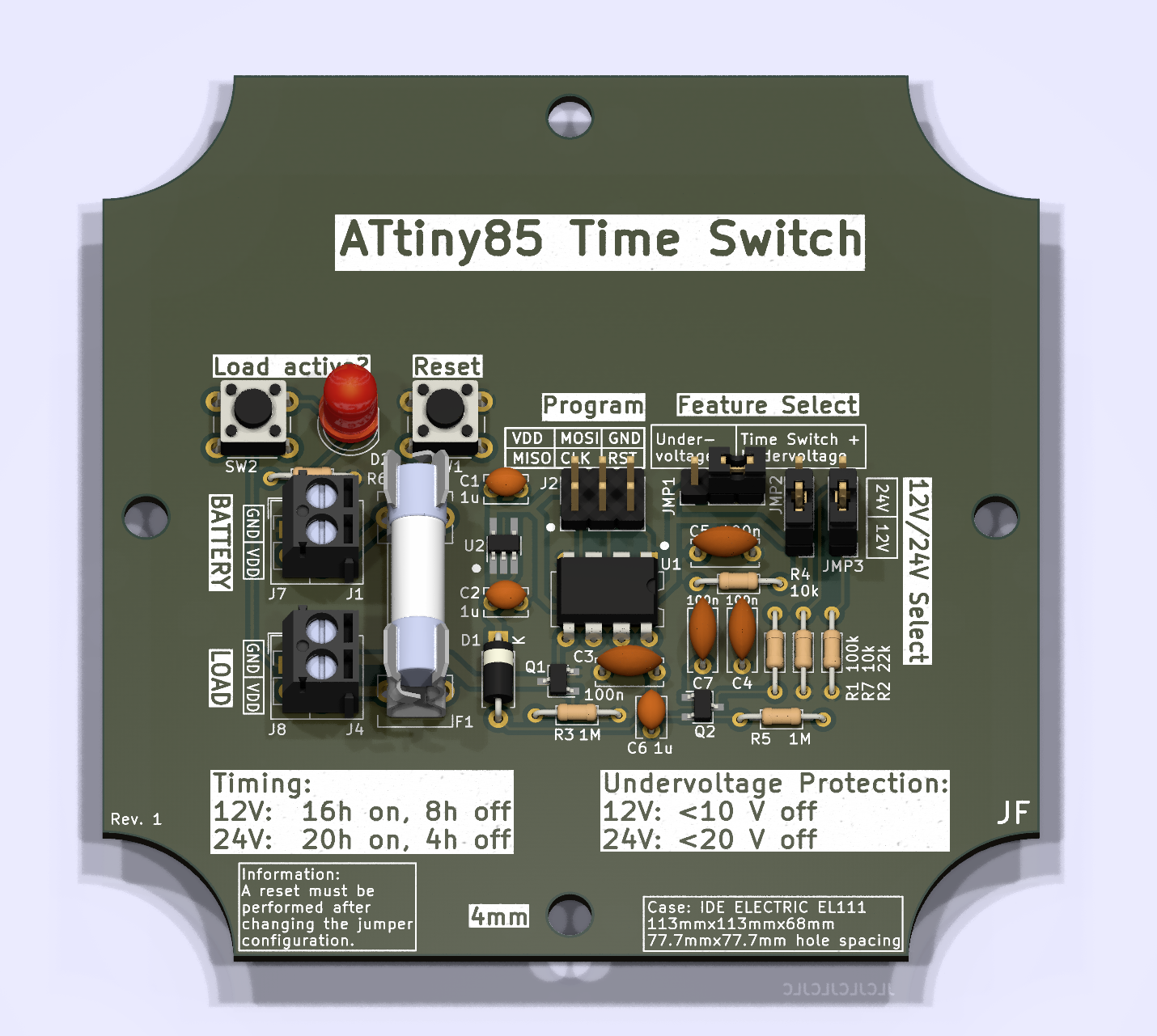
The aim of this project is to switch a load on and off in regular time intervals. The device itself consumes only very little sleep current (~19.6uA on average).
The device also monitors the supply voltage and turns off the load if the supply drops lower than the defined threshold.
| Type | Value |
|---|---|
| Average Current Consumption | 19.6uA |
| Maximum Load Current | 5.7A (cont.) |
| Supply Voltages | 12/24V |
| Switch Type | Low-Side |
There are three jumpers which must be set to either select the 12V or the 24V configuration. This changes the on/off times as well as the undervoltage thresholds.
Every time the jumper configuration is changed, a reset must be performed for the changes to take effect.
Upon coming out of reset, the device reads its clock calibration values stored in the internal eeprom to provide accurate timings for the time switch.
The device wakes up periodically and immediately goes back to sleep. That way, very long deep sleep periods can be reached.
The ATtiny85 runs off of the internal 128kHz low speed oscillator during deep sleep. The watchdog timer wakes up the device every 8.192s (the maximum watchdog timeout) and the ATtiny increments a counter variable.
If it surpasses a pre-defined threshold, the load switch changes state from on->off or the other way round.
Every 15 minutes it also measures the supply voltage and compares it to a pre-defined threshold. If the supply is lower than that threshold, the load is switched off until the device is reset.
The maximum load current is determined by the sizing of the n-fet Q1. With the n-fet PMV20XNER one can switch up to 5/7A. The load is switched with a low side switch.
The internal 8MHz oscillator of the ATtiny85 is used as the primary clock source. However, the clock frequency can vary by up to ±15%. In order to get accurate on/off times from the time switch, this internal oscillator must be calibrated. A detailed description of how to do that can be found here.
The pcb is designed to fit in the EL111 enclosure by IDE electric. It is screwed into the case using four M4 screws. The case itself is rated IP65-67. Its dimensions are 113x113x68 mm (Height x Width x Depth).
The code resides in the folder src and include. PlatformIO is chosen as the build environment. The best way to program the ATtiny85 is to use PlatformIO and VS Code as the IDE.
The pcb project can be found under pcb_project/attiny85_time_switch. The relevant code snippets for changing the timing values and the undervoltage thresholds are at the top of main.cpp.
The gerber files are in pcb_project/attiny85_time_switch/fabrication_outputs/.
| Qty | Value | Footprint | References |
|---|---|---|---|
| 4 | 100n | Capacitor_THT:C_Disc_D6.0mm_W2.5mm_P5.00mm | C3, C4, C5, C7 |
| 3 | 1u | Capacitor_THT:C_Disc_D3.8mm_W2.6mm_P2.50mm | C1, C2, C6 |
| 3 | Conn_01x03_Pin | Connector_PinHeader_2.54mm:PinHeader_1x03_P2.54mm_Vertical | J3, J5, J6 |
| 2 | 10k | Resistor_THT:R_Axial_DIN0204_L3.6mm_D1.6mm_P7.62mm_Horizontal | R4, R7 |
| 2 | 1M | Resistor_THT:R_Axial_DIN0204_L3.6mm_D1.6mm_P7.62mm_Horizontal | R3, R5 |
| 2 | Conn_01x02_Pin | Connector_PinHeader_2.54mm:PinHeader_1x02_P2.54mm_Vertical | J7, J8 |
| 2 | Screw_Terminal_01x02 | attiny85_time_switch:TerminalBlock_4Ucon_1x02_P3.50mm_Vertical | J1, J4 |
| 1 | 0751.0052 | attiny85_time_switch:0751.0052_Fuse | F1 |
| 1 | 100k | Resistor_THT:R_Axial_DIN0204_L3.6mm_D1.6mm_P7.62mm_Horizontal | R1 |
| 1 | 22k | Resistor_THT:R_Axial_DIN0204_L3.6mm_D1.6mm_P7.62mm_Horizontal | R2 |
| 1 | 3k3 | Resistor_THT:R_Axial_DIN0204_L3.6mm_D1.6mm_P7.62mm_Horizontal | R6 |
| 1 | AP7383-50W5-7 | Package_TO_SOT_SMD:TSOT-23-5_HandSoldering | U2 |
| 1 | ATtiny85V-10P | Package_DIP:DIP-8_W7.62mm | U1 |
| 1 | BSS84AK | Package_TO_SOT_SMD:TSOT-23 | Q2 |
| 1 | Check FET | Button_Switch_THT:SW_PUSH_6mm_H5mm | SW2 |
| 1 | Conn_02x03_Odd_Even | Connector_PinHeader_2.54mm:PinHeader_2x03_P2.54mm_Vertical | J2 |
| 1 | D | Diode_THT:D_A-405_P7.62mm_Horizontal | D1 |
| 1 | EL111 | attiny85_time_switch:Case EL111 | Case1 |
| 1 | LED | LED_THT:LED_D5.0mm | D2 |
| 1 | PMV20XNER | Package_TO_SOT_SMD:TSOT-23 | Q1 |
| 1 | Reset | Button_Switch_THT:SW_PUSH_6mm_H5mm | SW1 |
It measures 85.7 × 85.7 mm and has 2 copper layers, 1.6 mm thick.
32 parts, built around the ATTINY85V-10PU, FG18X5R1H105KRT06, BSS84AK,215(ES) and TL1105AF160Q. The full list of its parts is on this page, with links to each part's symbol and footprint where PCBKit's library has them.
From the UCSIG/attiny85_time_switch repository on GitHub, at the commit this page was made from: the board is pcb/attiny85_time_switch_rev1/attiny85_time_switch.kicad_pcb and its schematic pcb/attiny85_time_switch_rev1/attiny85_time_switch.kicad_sch. PCBKit opens the board in the browser, with nothing to install.
Its repository publishes it under the MIT licence: you may reuse it on that licence's terms (keep the author's notice, and for a copyleft licence share your changes alike).
pandemiaplan/OP-Vent
A Simple, Open-Source Ventilator using a Proportional Solenoid Valve

bitraf/toollock
Each lock has a key with a matching key pattern. The key is physically attached to the tool using a wire. An optical sensor detects that the right key is used.


Jjbinstock/RF-Clock-Generator
A dual channel, tunable RF clock generator PCB project

PTR-projects/PTR_arecorder
A compact, high-g flight data recorder designed specifically for model and amateur rocketry. The Arecorder logs 3-axis acceleration and orientation data to an SD card during launch, ascent, apogee, and recovery.

TheEinfachFelix/CampPhone
Warum habe ich mich dagegen entschieden, das Sim Modul selber zu implementieren? Ich habe kein Chip gefunden, der günstiger als das fertige Modul war, und ein Datenblatt in Englischer Sprache hat.

