Skip to the content
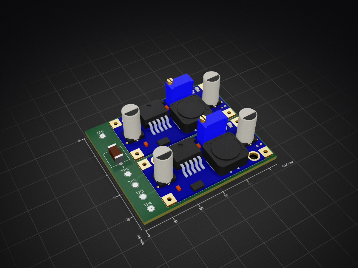
2 layers53.5 × 46 mmNodeNet PWR Module, the printed circuit board in 3D

Hello World project on Colorlight i9 FPGA

Size
53.5 × 46 mm
Copper layers
2
Thickness
1.6 mm
Parts
14
Nets
11
Pads
32
Tracks, vias
29, 5
Pours
1
Routed
Yes
KiCad
KiCad 10.0 (file 20260206)
Created
20 Jul 2026
Updated
10 Sep 2026

Overview

NodeNet PWR Module is an open-source printed circuit board by stephentissot, from the stephentissot/NodeNet-SoC-Risc-v repository on GitHub, published under the MIT licence. It is a 2-layer board of 53.5 × 46 mm with 14 parts on 11 nets, routed with 29 tracks and 5 vias.

It is built around the AO3407A, MF-LSMF185X-2 and SMBJ15A. Its parts include 2 capacitors, 1 resistor, 1 diode, 1 transistor and 1 fuse. It belongs with the fPGA and programmable logic boards of this library.

Main components

3

README

README.md

NodeNet SoC Risc-v — Colorlight i9 Multi-Node Embedded System

A complete RISC-V System-on-Chip (SoC) design for the Colorlight i9 FPGA board, featuring a PicoRV32 processor, Wishbone bus interconnect, persistent SPI flash storage, I2C peripherals, distributed RS485 multi-node communication via the NodeNet485 protocol, and a PLC runtime ready for relocatable object-file deployment.

Overview

This project demonstrates a scalable embedded systems design on a cost-effective FPGA:

  • Processor: PicoRV32 (32-bit RISC-V, bare-metal)
  • Clock: 25 MHz
  • Memory: 64 KiB ROM (stage0 bootloader) + 64 KiB RAM (stack/variables) + 8 MB SDRAM (runtime application/external data)
  • Peripherals: D2 LED GPIO, RJ45 LED pulse controllers (wb_led), UART1 Modbus RTU master (wb_modbus_master), RS485 NodeNet485, I2C master, SDRAM controller
  • Communication: NodeNet485 @ 1 Mb/s over RS-485 (multi-node capable)
  • Firmware: C++17, bare-metal, newlib-nano
  • Validated boot path: stage0 in ROM validates an image header in SPI flash, copies the payload to SDRAM, checks CRC, then jumps to the application entry point
  • Validated SDRAM path: full firmware execution from SDRAM, 32-bit accesses, partial Wishbone writes, linker-placed SDRAM_DATA variables, and scratch-area self-tests

Current project status:

  • PLC Ready with V0 basic ISA
  • runtime point catalog with pointDefsReq / pointStatesReq browsing and pagination
  • relocatable objectFileV1 PLC upload, firmware-side link/load, linked-bytecode readback, and object-file readback
  • 16 PLC slots with reboot persistence in the raw PLC flash package and automatic restore after boot
  • OLED boot progress screen plus post-boot slot status screen
  • ESP32 SPI coprocessor for local web API is in progress on the current branch; the shared SPI link, snapshot bootstrap, incremental state updates, and web UI runtime path are now working together on hardware, while broader validation and the MQTT bridge remain pending

Features

NodeNet PLC

  • NodeNet PLC catalog browsing supports pointDefsReq and pointStatesReq with hierarchical paths of the form deviceId.feature.pointId.
  • Point definitions can be created or updated with pointUpsert, and removed with pointDelete.
  • Modbus-backed points are polled by the PLC runtime and exposed through the same NodeNet command surface.
  • The PLC runtime publishes a shared SDRAM descriptor/value/status map, and PLC VM writes are consumed through the runtime write queue.
  • Generic PLC deployment uses relocatable objectFileV1 artifacts; the built-in plcLoadReq mirror helper remains available for fast validation.

PLC feature summary:

  • Main feature status: PLC Ready with V0 basic ISA
  • Runtime architecture: shared SDRAM PLC ABI, point runtime descriptors, value/status windows, slot loader/linker, persistent flash package restore at boot
  • Deployment model: host builds relocatable objectFileV1, firmware links it against the live point catalog, loads it into one of 16 slots, and can persist the slot set for reboot restore
  • Operating surface: NodeNet browse/update commands for point definitions and point states, PLC slot control/status points, raw PLC upload flow, linked-bytecode readback, and original object-file readback

PLC documentation index:

NodeNet Validation Snapshot (2026-08-20)

  • Automatic heartbeat in HDL validated on hardware at ~10 s period.
  • RX to local address validated (message accepted and decoded).
  • TX path validated end-to-end.
  • Runtime baud operation validated at both 115200 and 1 Mb/s.
  • RX metadata is propagated end-to-end (src, dst, broadcast, len).
  • Distinct PicoRV32 IRQs exist for broadcast vs unicast RX and are consumed through firmware callbacks.
  • ROM stage0 now forwards the fixed IRQ vector at 0x00000004 to the SDRAM app IRQ entry.

FlashDB Validation Snapshot (2026-08-13)

  • Flash low-level test passes at boot ([FLASH] LowLevel PASS).
  • FlashDB initialization passes ([FDB] Ready).
  • Boot counter write path passes ([FDB] boot cnt updated).

Hardware

  • Wishbone B.4 Bus interconnect with 32-bit data, 32-bit address
  • PicoRV32 Core: Open-source RISC-V ISA, ~6K LUT footprint
  • Memory Map:
    • 0x00000000–0x0000FFFF: 64 KiB boot ROM (stage0 bootloader)
    • 0x00010000–0x0001FFFF: 64 KiB RAM (stack, BSS, heap)
    • 0x10000000: D2 LED GPIO (1-bit output)
    • 0x10000004: RJ45 LED0 (wb_led one-shot pulse)
    • 0x10000008: RJ45 LED1 (wb_led one-shot pulse)
    • 0x10004000: UART1 Modbus RTU master (wb_modbus_master)
    • 0x10005000: I2C0 master (8 registers @ 4-byte stride)
    • 0x10006000: NodeNet485 RS-485 mailbox (8 registers, 1 Mb/s)
    • 0x20000000–0x207FFFFF: 8 MB SDRAM (runtime application image / framebuffer / logs)

Peripherals

  • NodeNet485 Module (wb_nodenet.sv):

    • Multi-node RS-485 communication protocol
    • Baud rate: runtime divisor (validated at 115200 and 1 Mb/s)
    • HDLC-style framing with parity bits and CRC
    • Mailbox-based Wishbone interface for TX/RX messages
    • Internal message buffering (no external SDRAM FIFO usage)
    • Anti-collision backoff (address-based delay)
    • Periodic heartbeat for node discovery
    • Priority-based transmission (LOW/NORMAL/HIGH)
    • Full C++ firmware API in src/firmware/lib/nodenet/nodenet.h
    • Supports unicast, broadcast, and heartbeat messages
    • Supports callback-driven broadcast / unicast reception on PicoRV32 IRQs
    • RX decode error reporting and TX scheduling status
    • Wishbone register interface (0x10006000)
  • I2C Module (wb_i2c.sv):

    • Wraps Alex Forencich's i2c_master_wbs_16 core
    • Hardware command + write + read FIFOs (32 entries each)
    • Configurable speed (default 100 kHz, up to 400 kHz @ 25 MHz)
    • Drives SCL/SDA open-drain (external 4.7 kΩ pullup required)
    • Wishbone address: 0x10005000
  • Modbus Master Module (src/modbus/wb_modbus_master.sv):

    • Wishbone Modbus RTU master transaction engine
    • Uses shared uart_simple.sv UART core for wire-level TX/RX
    • Hardware-managed CRC16 (TX generation + RX validation)
    • Hardware-managed RTU frame gap detection (inter-frame silence)
    • Retries, timeout, and status/error flags exposed through MMIO
    • Firmware API in src/firmware/lib/modbus/ModbusMaster.{h,cpp}
    • Wishbone address: 0x10004000
  • SPI Flash Module (wb_flash.sv, spi_master.sv):

    • Wishbone interface to on-board SPI flash (W25Q64, 8 MB)
    • Memory layout: 2 MB boot config (protected) + 12 KB point catalog + 4 KB compatibility gap + 128 KB PLC package + 124 KB FlashDB KV + 4 KB self-test scratch + app data
    • C++ firmware uses low-level page/sector API (Flash) plus FlashDB wrapper (flashdb_port)
    • Exposes the factory-programmed 64-bit Winbond UID as a stable ASCII device ID
    • Boot region protection: firmware rejects writes/erases to 0x000000–0x1FFFFF
    • Point catalog storage at 0x200000–0x202FFF (12 KB, 3 sectors)
    • Compatibility gap at 0x203000–0x203FFF (4 KB)
    • Persistent PLC package at 0x204000–0x223FFF (128 KB)
    • FlashDB KV partition at 0x224000–0x242FFF (124 KB)
    • Flash low-level self-test scratch at 0x243000–0x243FFF (4 KB)
    • Wishbone address: 0x10007000
    • See src/wbDevices/README_FLASH.md for details

Firmware

  • C++17 bare-metal (firmware/main.cpp):

    • Compiled with riscv-none-elf-g++ — no Arduino, no OS
    • newlib-nano provides memcpy/strlen/etc.
    • Dead code elimination (-ffunction-sections -Wl,--gc-sections)
    • Global C++ constructors called in start.S via .init_array
    • Final runtime image is linked for SDRAM via link_app_sdram.ld
    • Loaded by ROM-resident boot_stage0 from SPI flash offset 0x244000
    • Includes ArduinoJson 7 in freestanding mode, with an optional SDRAM-backed allocator for large JSON payloads
    • NodeNet485 callback flow: receives broadcast/unicast events through IRQ callbacks and defers heavy work to the main loop
    • D2 activity heartbeat: non-blocking software toggle every 500 ms
  • External SDRAM bring-up:

    • Cold boot initialization now follows the generated LiteDRAM DFII sequence before the SDRAM user port is released
    • Firmware should still call sdram_wait_ready() before touching SDRAM_DATA objects or the JSON SDRAM pool
  • See src/firmware/README.md for full peripheral usage guide.

  • See src/wbDevices/README_NODENET.md for protocol details.

  • See src/modbus/README.md for Modbus RTU master details.

  • See src/wbDevices/README_FLASH.md for flash UID and device ID details.

Building

Prerequisites

  • Yosys (synthesis)
  • NextPNR (place & route)
  • ecppack (bitstream generation)
  • RISC-V GCC toolchain (riscv-none-elf-gcc ≥ 12, with C++ support)
  • Make

After cloning, fetch the u8g2 submodule:

bash
git submodule update --init

Build Steps

bash
# Full build (firmware + FPGA)
make all

# Stage0 bootloader only (ROM image)
make firmware-bootloader

# Alias: same stage0 ROM build as above
make firmware-build

# Build stage0 application image (SDRAM payload + header in SPI flash format)
make firmware-image

# SDRAM application ELF only
make -C src/firmware firmware-app-build

# Program firmware payload only in SPI flash (no FPGA rebuild)
make flash-fw

# If bootloader ROM startup / IRQ forwarding changed, reload the FPGA image too
make ram

# Optional: enforce openFPGALoader verify as fatal
make FW_STRICT_VERIFY=1 flash-fw

make firmware-build / make firmware-bootloader print stage0 ROM size telemetry on each build:

  • ELF text/data/bss
  • RAM usage (.data + .bss)
  • HEX file size and payload bytes
  • ROM usage (payload / ROM_BYTES, in %)

If payload exceeds ROM capacity, build stops with an explicit error.

CPU profile note:

  • Default build is configured in fast mode for PicoRV32 in src/top.sv with:
    • .BARREL_SHIFTER(1)
    • .ENABLE_FAST_MUL(1)
    • .ENABLE_DIV(1)
  • To switch back to the normal/smaller CPU profile, set those three parameters to 0 in src/top.sv and rebuild (make clean; make).

If OpenOCD flash programming fails on your setup, you can switch the flash targets in Makefile to ecpdap. Reference commands:

make
# ecpdap fallback examples (Colorlight i5/i9 style headers)
# flash:
# 	ecpdap flash unprotect
# 	ecpdap flash write build/top.config
#
# unlock-flash:
# 	ecpdap flash unprotect
#
# lock-flash:
# 	ecpdap flash protect

Output:

  • src/firmware/build/boot_stage0.hex – Stage0 bootloader image (loaded into ROM, includes IRQ forward stub to the SDRAM app)
  • src/firmware/build/nodenet_riscv_app.img – SDRAM app payload with stage0 header (written in SPI flash at 0x244000)
  • build/top.bit – FPGA bitstream (~300 KB)
  • build/top.json – Netlist (debug/inspection)

Memory Layout

text
Address Range               Size      Purpose
────────────────────────────────────────────────────────────
0x00000000–0x0000FFFF     64 KiB   Boot ROM (stage0 bootloader)
0x00010000–0x0001FFFF     64 KiB   RAM (stack, BSS, heap)
────────────────────────────────────────────────────────────
0x10000000                4 B      D2 LED GPIO (bit [0] = LED output)
0x10000004                4 B      RJ45 LED0 (`wb_led` control/status)
0x10000008                4 B      RJ45 LED1 (`wb_led` control/status)
0x10004000                32 B     UART1 Modbus RTU master (`wb_modbus_master`)
0x10005000                32 B     I2C0 master (8 regs @ 4-byte stride)
0x10006000–0x1000601F     32 B     NodeNet485 mailbox + LED config (RS485, 1 Mb/s)
0x10007000                32 B     SPI Flash controller (W25Q64)
────────────────────────────────────────────────────────────
0x20000000–0x207FFFFF     8 MB     SDRAM — Runtime app image + large buffers/logs
────────────────────────────────────────────────────────────
0x00000000–0x1FFFFF       2 MB     SPI Flash — FPGA boot config (PROTECTED)
0x200000-0x202FFF         12 KB    SPI Flash — Point catalog
0x203000-0x203FFF         4 KB     SPI Flash — Compatibility gap / reserved
0x204000-0x223FFF         128 KB   SPI Flash — Persistent PLC package
0x224000-0x242FFF         124 KB   SPI Flash — FlashDB KV partition
0x243000-0x243FFF         4 KB     SPI Flash — Flash low-level self-test scratch
0x244000–0x7FFFFF         5.73 MB  SPI Flash — Stage0 application image slot

Boot Flow

  1. FPGA configuration loads the SoC bitstream and the wb_rom contents containing boot_stage0.
  2. Stage0 starts from 0x00000000, initializes required peripherals, and reads the application header from SPI flash offset 0x244000.
  3. Stage0 validates header fields and CRCs, copies the application payload into SDRAM at 0x20000000, then jumps to the image entry point.
  4. PicoRV32 IRQ entry remains fixed at 0x00000004; the ROM image forwards that vector to the SDRAM application IRQ entry at 0x20000004.
  5. The runtime firmware executes entirely from SDRAM, while SPI flash remains available for parameter storage, FlashDB, and firmware updates.
  6. SDRAM self-tests used by the runtime stay inside a reserved scratch area so they do not overwrite the executing image.

Device Pinout

RS485 (NodeNet485 Protocol)

  • Pins: G5 (RX), D16 (TX)
  • Baud Rate: 1 Mb/s (fixed, configurable via UART parameter)
  • Protocol: Multi-node RS-485 with HDLC framing, anti-collision, heartbeat
  • Transceiver: Any RS-485 module with auto-switching (MAX485, SN65HVD11, etc.)
  • Multi-Node: Up to 20 nodes on shared bus with address-based scheduling
  • Features: Parity-encoded payload (2x expansion), XOR CRC, priority levels (LOW/NORMAL/HIGH), heartbeat
  • Connector topology: 2x RJ45 in daisy-chain (IN/OUT), wired pin-to-pin between connectors

NodeNet RJ45 pinout (both connectors):

RJ45 PinSignal
1+12V
2+12V
3RS485 A
4GND
5GND
6RS485 B
7GND
8GND

I2C (D18/D17 pins)

  • SCL: D18
  • SDA: D17
  • Requires external 4.7 kΩ pullup resistors to 3.3 V on both lines
  • Compatible with any I2C device: OLED, sensors, ADC, GPIO expanders…

GPIO

  • D2 LED: GPIO output at 0x10000000 (bit [0] = LED state)

RJ45 LEDs (wb_led)

  • LED0 (F5): 0x10000004
  • LED1 (E6): 0x10000008
  • Active-low wiring policy: GPIO high = LED OFF, GPIO low = LED ON.
  • LPF enables pull-up on these pins for deterministic OFF level during startup.
  • Write command bit0 triggers a non-blocking pulse (duration can be overridden by firmware).
  • RJ45 LEDs are available through wb_led and can be used by application firmware when needed.

NodeNet Activity LEDs (100% hardware)

  • RX activity LED (E5, green): default ON, pulses OFF when a valid frame is received.
  • TX activity LED (F4, orange): pulses ON when a transmission is queued.
  • Active-low with pull-up: idle/high keeps LED OFF unless logic drives low.
  • Blink duration is configured by firmware through NodeNet register 0x1000601C (milliseconds).

SPI Flash (W25Q64)

  • Pins: R2 (CS), W2 (MOSI), V2 (MISO)
  • Clock: Generated internally (10 MHz typical, no GPIO pin)
  • Capacity: 8 MB (2 MB boot + 16 KB params + 256 KB FlashDB KV + ~5.73 MB app)
  • Boot Protection: Firmware API rejects writes to 0x000000–0x1FFFFF
  • Parameter Region: 0x200000–0x203FFF (raw/scratch area)
  • FlashDB KV Region: 0x204000–0x243FFF (nodenet_kv partition)

Firmware Examples

See src/firmware/README.md for a full guide with code examples for every peripheral.

Quick-start: UART1 Modbus RTU master

cpp
#include "ModbusMaster.h"

constexpr uint32_t MODBUS1_BASE = 0x10004000u;
constexpr uint8_t MODBUS_SLAVE = 0x01u;
ModbusMaster modbus1(MODBUS1_BASE);

int main() {
  modbus1.begin(9600, 500, 2);
  modbus1.setInterframeCharsQ1(14);

  uint16_t version = 0;
  if (modbus1.readHoldingRegisters(MODBUS_SLAVE, 0x8000, 1, &version)) {
    // 0x0064 => V1.00
  }

  for (;;) {
    // Toggle channel 1 (coil address 0)
    (void)modbus1.writeSingleCoil(MODBUS_SLAVE, 0x0000, true);
  }
}

Quick-start: NodeNet echo

cpp
#include <stdint.h>
#include "nodenet.h"

#define LED          (*(volatile uint32_t*)0x10000000)
constexpr uint32_t NODENET0_BASE = 0x10006000u;

int main() {
  NodeNet myNodeNet(NODENET0_BASE, 0x01, NODENET_PRIORITY_NORMAL, 200);
  for (;;) {
    if (myNodeNet.HasMessage()) {
      NodeNetMessage msg = myNodeNet.ReadMessage();
      if (msg.src_addr != 0) {
        myNodeNet.Send(msg.src_addr, msg.data, msg.len);
      }
      NodeNet::FreeMessage(msg);
    }
    LED ^= 1;
  }
}

Quick-start: OLED via u8g2

cpp
#include "u8g2_hal.h"

u8g2_t display;

int main() {
    u8g2_Setup_ssd1306_i2c_128x64_noname_f(
        &display, U8G2_R0,
        u8x8_byte_i2c_hw,
        u8x8_gpio_delay_hw);
    u8g2_InitDisplay(&display);
    u8g2_SetPowerSave(&display, 0);
    u8g2_ClearBuffer(&display);
    u8g2_SetFont(&display, u8g2_font_ncenB08_tr);
    u8g2_DrawStr(&display, 0, 12, "RISC-V SoC");
    u8g2_SendBuffer(&display);
    for (;;);
}

Wishbone Bus Modules

See src/wbDevices/README.md for detailed documentation of each Wishbone peripheral module.

Resource Usage

Lattice LFE5U-45F-6BG381C (Colorlight i9):

  • Total LUTs: 45K
  • Block RAM (DP16KD): 108 (each 16K bits)
  • Current design:
    • PicoRV32: ~6K LUT
    • Interconnect: ~1K LUT
    • ROM (64 KiB): 32 blocks
    • RAM (64 KiB): 32 blocks
    • NodeNet485 transport + UART: ~300 LUT
    • SDRAM controller: ~400 LUT
    • GPIO: ~50 LUT
    • Total: ~35% of available resources

Architecture

text
                   +----------------+
                   |   PicoRV32     |
                   +-------+--------+
                           |
                      Wishbone B4
                           |
      +--------+-----------+---------+--------+----------+-------+
      |        |           |         |        |          |       |
      wb_rom  wb_ram  wb_modbus_master  wb_nodenet wb_gpio wb_led wb_sdram wb_i2c
            |         |
            uart_simple  uart_simple
                 |
               NodeNet framing
        LED D2   RJ45 LEDs   M12L64322A  SSD1306   W25Q64
              |                    (8MB SDRAM) OLED
            RS485 Transceiver
                           |
                 Direct RS485 A/B/GND
                           |
                   Field Connectors

Data Flow:

  1. Power-up / stage0: wb_rom exposes the 64 KiB ROM image containing boot_stage0, which loads and validates the SDRAM application stored in SPI flash.
  2. Runtime CPU (PicoRV32): 32-bit RISC-V, 25 MHz clock, executing the main firmware from SDRAM after stage0 handoff.
  3. Wishbone B.4 Bus: 32-bit address, 32-bit data, address decoder for memories and peripherals.
  4. Memory & I/O:
  • wb_rom: 64 KiB boot ROM for stage0 only (0x00000000)
  • wb_ram: 64 KiB RAM (0x00010000)
  • wb_sdram_litedram: 8 MB SDRAM runtime memory window (0x20000000)
  • wb_flash: SPI flash control + persistence services (0x10007000)
  • wb_modbus_master: Modbus RTU master transport (0x10004000)
  • wb_nodenet: NodeNet485 mailbox transport (0x10006000)
  • wb_gpio: D2 GPIO output (0x10000000)
  • wb_led: RJ45 LED pulse controllers (0x10000004 / 0x10000008)
  • wb_i2c: I2C master with FIFOs (0x10005000)
  1. NodeNet Transport: Mailbox-driven TX/RX framing, decode, and heartbeat scheduling.
  2. I2C Core: Wraps Alex Forencich's i2c_master_wbs_16 with Wishbone interface.
  3. RS485 Physical: Transceiver converts CMOS <-> RS485 differential signaling.
  4. Field Wiring: Each RS485 channel is exposed as direct A/B/GND connections.

Planned Enhancements

  • 8 MB SDRAM controller (wb_sdram_litedram.sv) with LiteDRAM-generated core and runtime execution from SDRAM
  • I2C master (wb_i2c.sv) — Wishbone wrapper around verilog-i2c
  • u8g2 OLED display support (SSD1306 128×64 over I2C)
  • C++17 firmware with newlib-nano and dead-code elimination
  • SDRAM section in linker script (sdram.h, SDRAM_DATA macro)
  • NodeNet485 mailbox transport with TX/RX framing and heartbeat (validation pending)
  • UART1–4 implementation and testing
  • RS485 direct connector mapping and labeling verification (A/B/GND)
  • wb_gpio control bit for RS485 120R termination switch (74LVC1G66GW,125)
  • Modbus V1 front-end: 4x RS485 modules with direct A/B/GND connectors per channel
  • wb_gpiopwm peripheral + firmware API (PKLCS1212E4001-R1 buzzer)
  • TMP117 board temperature sensor + firmware I2C driver/API
  • Display validation: OLED over I2C and LCD over SPI (select final path after tests)
  • Evaluate and select more robust 1 Mb/s transceivers for Modbus and NodeNet
  • Dual Ethernet breakout using i9 onboard Broadcom PHYs (2x RJ45 with magnetics)
  • RJ45 LEDs integrated through wb_led at dedicated addresses
  • Final RJ45 firmware policy (link/activity/status) for production runtime
  • ESP32 module SPI coprocessor for web API and MQTT bridge (in progress: shared SPI link, HTTP app, websocket updates, and plcLink snapshot/resync path validated on hardware; MQTT bridge still pending)
  • Power option study: use ESP32 module 3.3V rail vs dedicated 12V->3.3V buck
  • Modbus RTU master module + firmware driver (wb_modbus_master + ModbusMaster)
  • Modbus RTU slave mode
  • NodeNet JSON protocol wrapper (UART4)
  • SPI slave interface for ESP32 co-processor
  • SPI color LCD support (ST7789, 76x284) on Colorlight i9
  • KNX integration with NCN5120 transceiver module
  • Hardware-based CRC accelerator
  • Real-time interrupt controller (RISC-V PLIC)

Hardware Requirements

  • Colorlight i9 Board with Lattice LFE5U-45F FPGA
  • USB-C Programmer (e.g., openFPGALoader, oss-cad-suite)
  • RS485 Transceiver modules (SN65HVD230, MAX483, etc.)
  • RS485 Field Connectors (A/B/GND per channel)
  • SSD1306 OLED Module (I2C, 128×32 or 128×64) + 4.7 kΩ pullup resistors

Testing

bash
# Program RAM (requires openFPGALoader)
make ram

# Program Flash (permanent)
make flash

# Explicit flash protection control (optional)
make unlock-flash
make lock-flash

# UART loopback test
# - Send "Hello" via USB-to-UART adapter
# - LED should blink
# - Characters echoed back

make flash now performs an explicit unlock step in the OpenOCD write command (flash write_image erase unlock ...) before erase/program. make lock-flash/make unlock-flash call flash protect ... through OpenOCD; effectiveness/persistence depends on driver support for the target flash path.

References

License

See LICENSE file.

Author

Stephen Tissot
Industrial IoT / FPGA Engineering
https://github.com/stephentissot


Status: Prototype / Active Development
Last Updated: 2026-08-18

Parts

14
QtyValueFootprintReferences
1100 uF 25VMyLibrary:PCAP_6.3x7.7-ELECT_NCAC2
1100KResistor_SMD:R_1206_3216MetricR1
1100nF 50VCapacitor_SMD:C_1206_3216MetricC1
112VTestPoint:TestPoint_Pad_D2.0mmTP1
112V 3.3V buck converterMyLibrary:CONV_MC00100PS2
112V 5V buck converterMyLibrary:CONV_MC00100PS1
112VInTestPoint:TestPoint_Pad_D2.0mmTP5
13.3VTestPoint:TestPoint_Pad_D2.0mmTP3
15VTestPoint:TestPoint_Pad_D2.0mmTP2
1AO3407APackage_TO_SOT_SMD:SOT-23Q1
1ByPassJumper:SolderJumper-2_P1.3mm_Open_RoundedPad1.0x1.5mmJP1
1GNDTestPoint:TestPoint_Pad_D2.0mmTP4
1MF-LSMF185X-2Fuse:Fuse_2920_7451MetricF1
1SMBJ15AMyLibrary:SMBJ15AD1

Similar boards

  • 2 layers50 × 50 mmMotor driver, the printed circuit board in 3D

    Motor driver

    Dhruv2212-star/Motor-driver

    it is a very simple motor driver that will recive the data from another micro-controller

    14 parts
  • 6 layers36 × 124 mmOpenDual Reader, the printed circuit board in 3D

    OpenDual Reader

    nuerolynx/embedded-systems-lab

    Arduino UNO R4 WiFi and ESP32 prototypes for access control, automation, displays, monitoring, and Bluetooth audio.

    74 parts4
  • 8 layers217.5 × 187.5 mmBoard c openroute partial, the printed circuit board in 3D

    Board c openroute partial

    ajisrawi/passive-radar-counter-drone

    Passive radar for counter-drone using DVB-T, 4G and 5G: simulation, receiver hardware, FPGA micro-Doppler firmware, antennas, enclosure

    314 parts3
  • 2 layers170.6 × 121.1 mmEIM, the printed circuit board in 3D

    EIM

    bhorst519/bluecar

    232 parts3
  • 4 layers220 × 120 mmCandidate filled profile, the printed circuit board in 3D

    Candidate filled profile

    misko/prompt2device

    The separate vNext PCB skill and orchestrator package is available alongside the reference workflow below; existing projects keep their accepted toolchain until an explicit migration.

    569 parts3MIT
  • 4 layers100 × 100 mmPCB Design, the printed circuit board in 3D

    PCB Design

    ConquerToFreedom/SwasthEdge

    Low-cost self-diagnosing edge controller for industrial sensor reliability

    89 parts2
  • 4 layers150 × 112 mmBoard v3-83pct, the printed circuit board in 3D

    Board v3-83pct

    dmz006/brain-drain

    Standalone four-bay (plus M.2) NIST 800-88 disk sanitizer: Raspberry Pi CM5 carrier board, Python service, 3D-printed enclosure

    302 parts2
  • 6 layers268 × 230 mmRf board, the printed circuit board in 3D

    Rf board

    PE1RGU/hf-antenna-switch

    Remote HF antenna switch: 3 radios x 4 antennas (path to 8), outdoor relay unit with a hardware safety chain, controlled over Cat6 from a shack interface. KiCad 10, open hardware, designed together with an AI.

    357 parts2CERN-OHL-S-2.0

Questions

How big is the NodeNet PWR Module PCB?

It measures 53.5 × 46 mm and has 2 copper layers, 1.6 mm thick.

What parts does the NodeNet PWR Module use?

14 parts, built around the AO3407A, MF-LSMF185X-2 and SMBJ15A. The full list of its parts is on this page, with links to each part's symbol and footprint where PCBKit's library has them.

Where can I download the NodeNet PWR Module KiCad files?

From the stephentissot/NodeNet-SoC-Risc-v repository on GitHub, at the commit this page was made from: the board is src/hardware/NodeNetSoh_motherboard_V0.1/Modules/NodeNet_PWR_Module/NodeNet_PWR_Module.kicad_pcb and its schematic src/hardware/NodeNetSoh_motherboard_V0.1/ColorLight i9.kicad_sch. PCBKit opens the board in the browser, with nothing to install.

Can I use the NodeNet PWR Module design in my own project?

Its repository publishes it under the MIT licence: you may reuse it on that licence's terms (keep the author's notice, and for a copyleft licence share your changes alike).