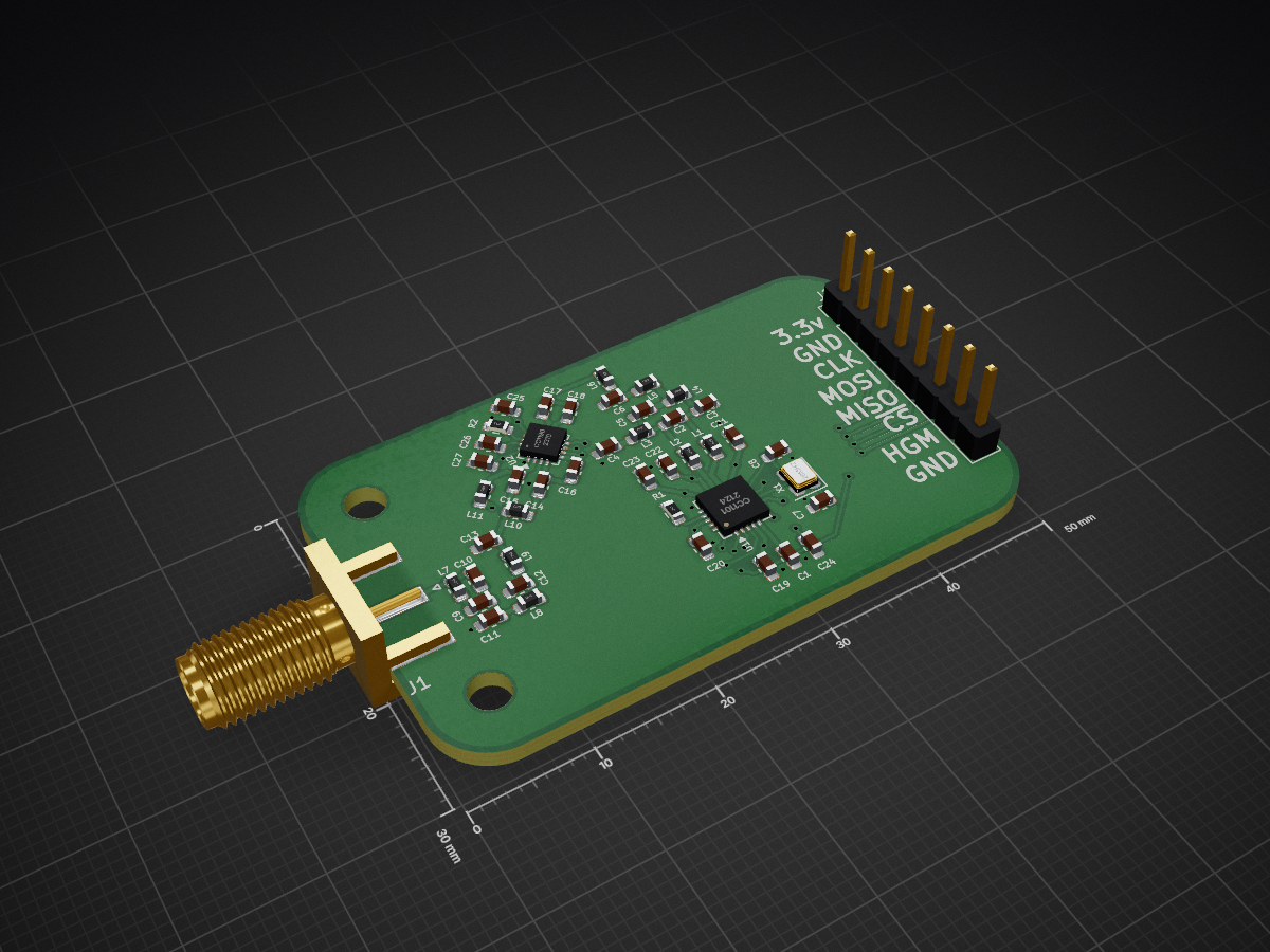
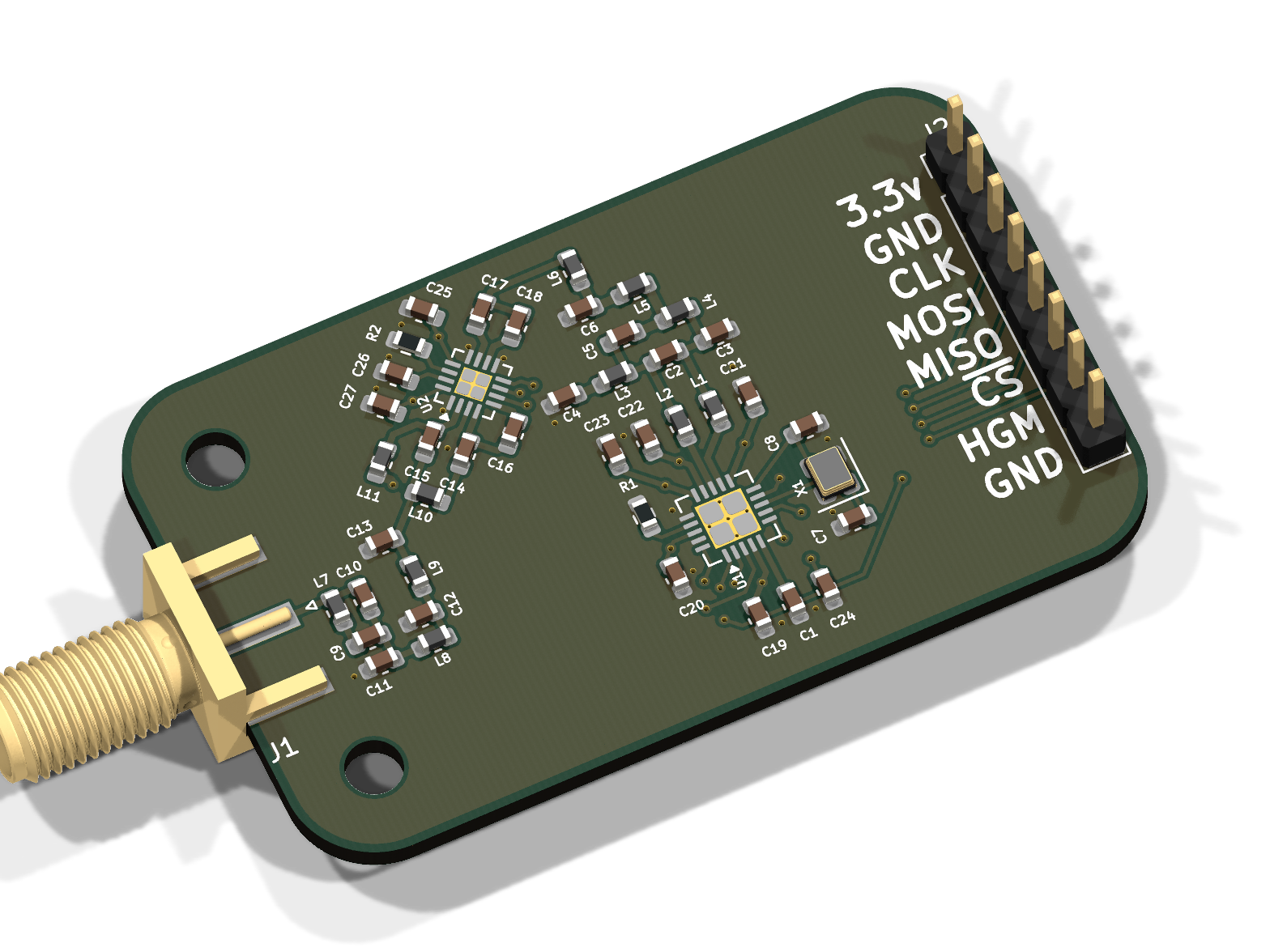
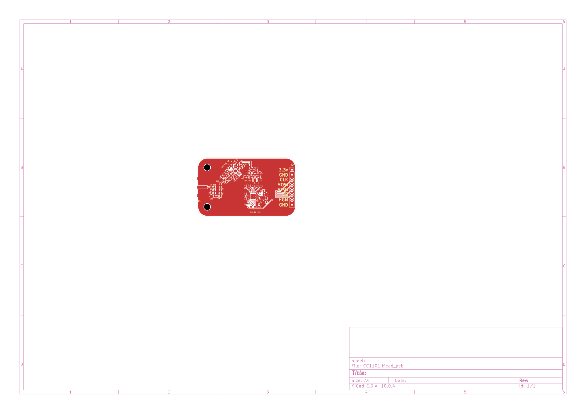
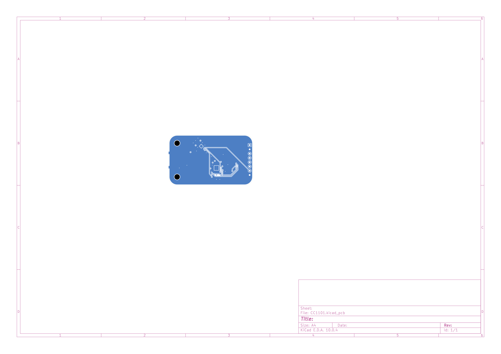
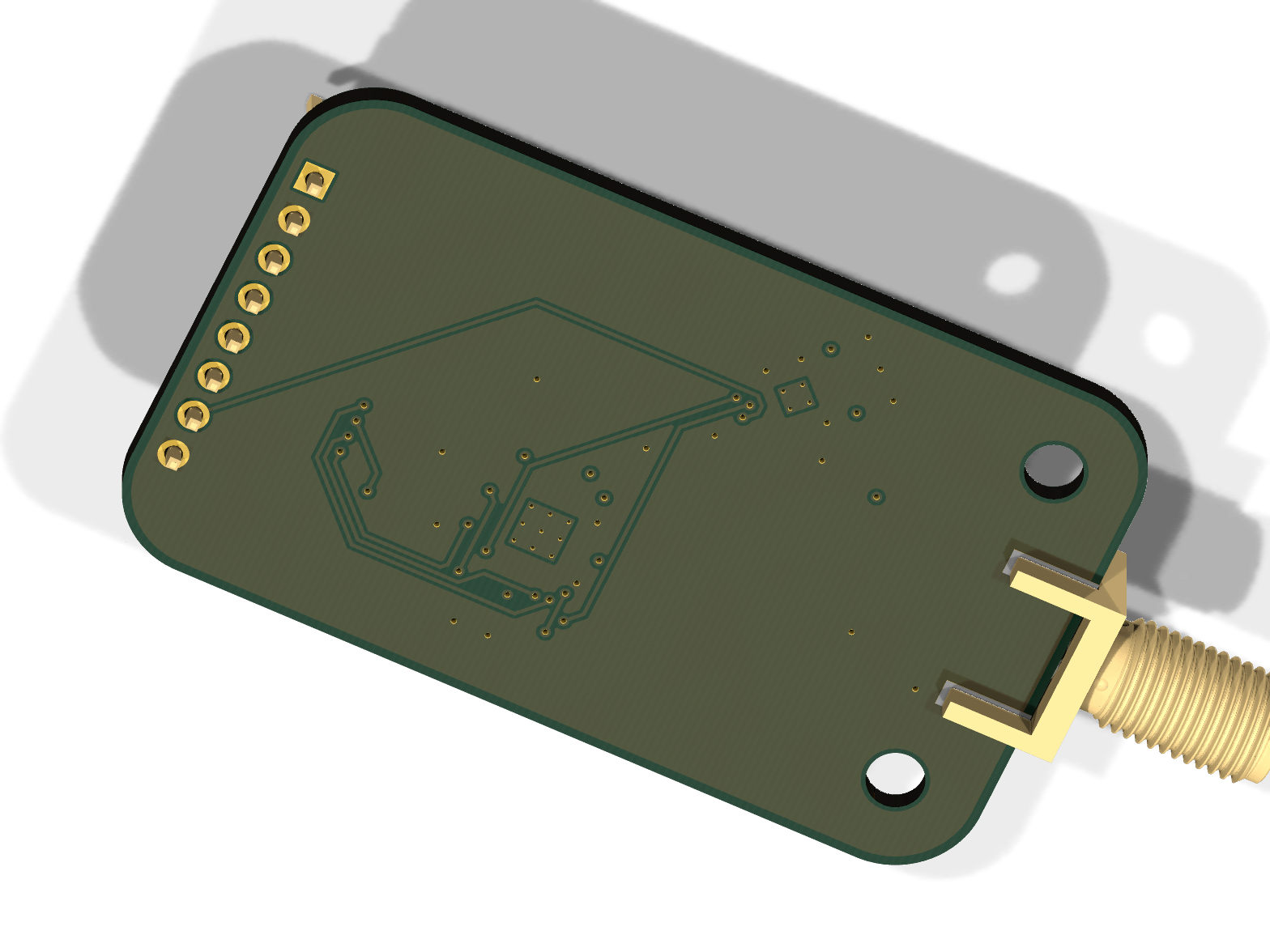
CC1101 is an open-source printed circuit board by sneakylizard123-4, from the sneakylizard123-4/CC1101_Module repository on GitHub, published under the CERN-OHL-P-2.0 licence. It is a 4-layer board of 50 × 30 mm with 47 parts on 33 nets, routed with 208 tracks and 43 vias.
It is built around the CC1101RGP and CC1190. Its parts include 27 capacitors, 11 inductors, 2 resistors, 2 ICs and 2 connectors. It belongs with the radio and wireless boards of this library.
A 868/915 MHz sub-GHz radio module built around the TI CC1101 transceiver and a CC1190 PA/LNA front end, on a hand-routed 4-layer board.
A simple breakout-style radio module for long-range sub-GHz link without designing an RF front end from scratch.
An SPI header brings the CC1101 onto any microcontroller bus, and the CC1190 adds a power amplifier and low-noise amplifier between the transceiver and an edge-mount SMA.
Custom Features
CC1101 + CC1190 combo - the CC1190 front end adds up to +20 dBm TX power and a low-noise receive path, which is a meaningful power and range increase over a bare CC1101 module.
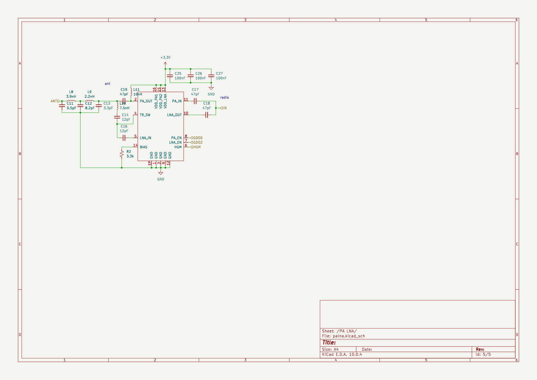
Hardware TX/RX switching - the CC1101 GDO0 and GDO2 pins drive CC1190 PA_EN and LNA_EN directly, so the front end follows the radio state with no firmware intervention.
Single 3.3 V rail - no regulator or level shifter on board; the module expects clean 3.3v.
10 x 100 nF decoupling - one decoupling capacitor plus nine supply decoupling capacitors spread around the two QFN packages.
4-layer - solid ground plane, short RF paths, and 43 stitching vias. No autorouter was used.
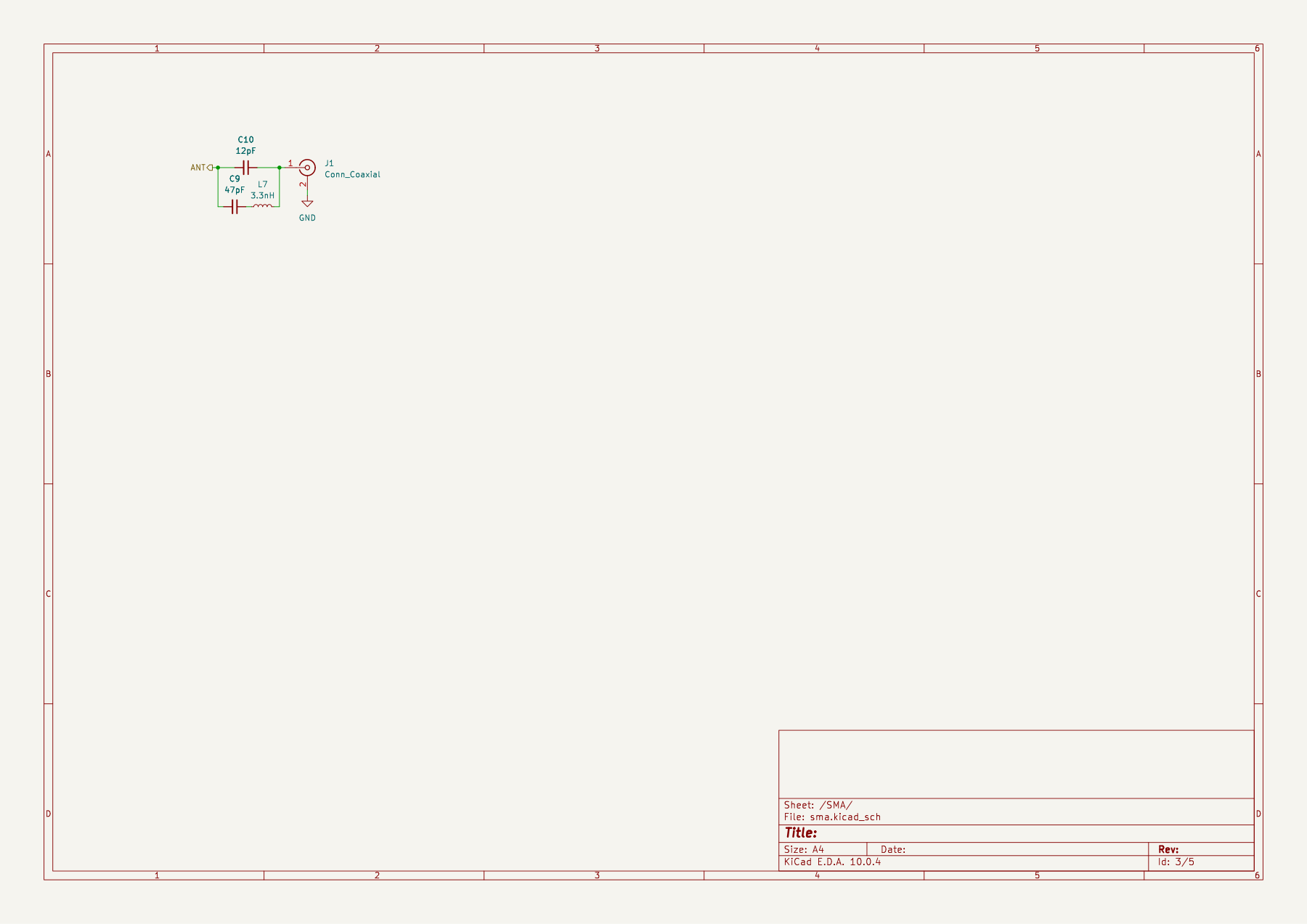
Edge-mount SMA with the RF match kept close to the connector.
Two M3 mounting holes so the module can be screwed into an enclosure or carrier board.
How It Works
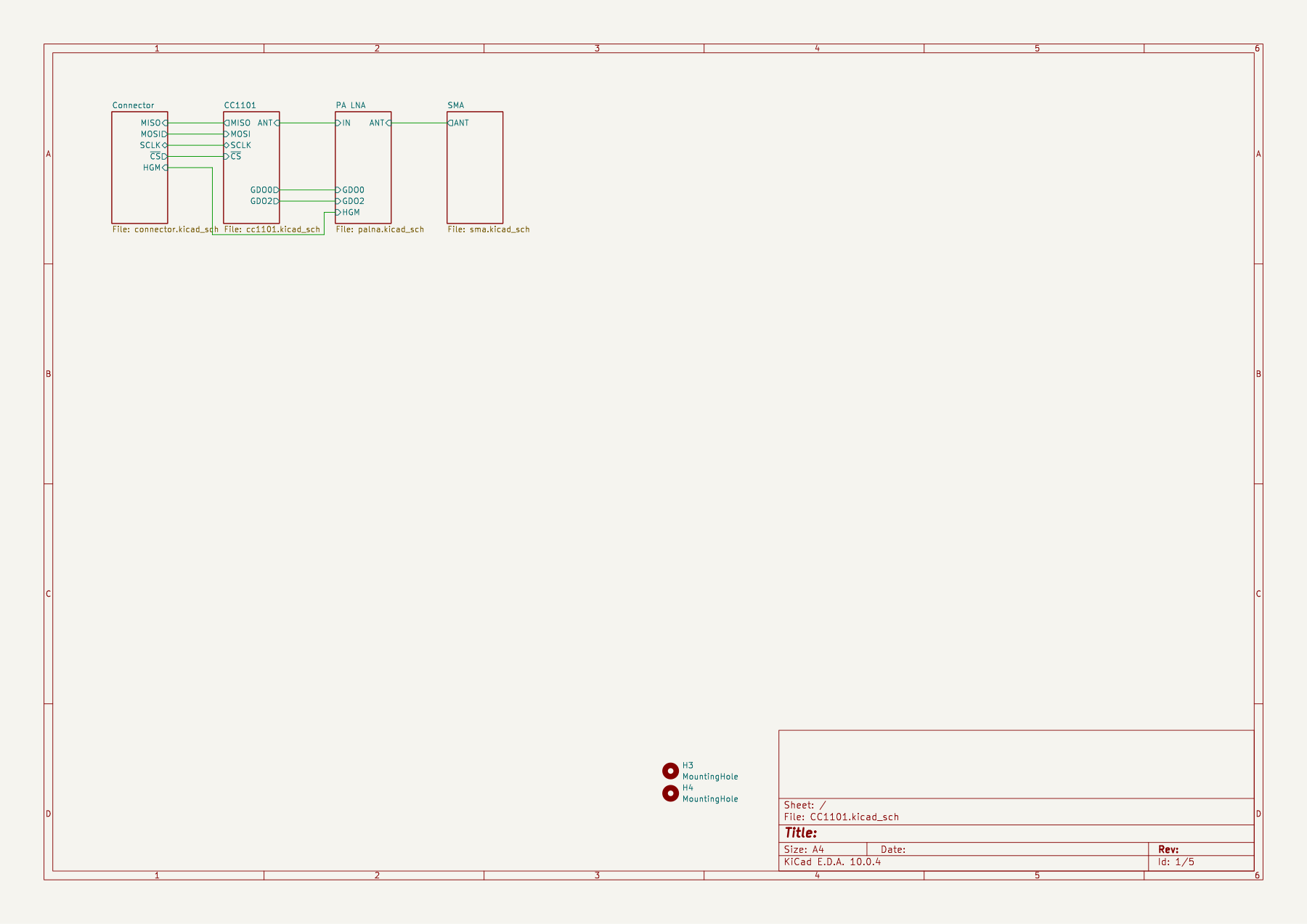
The module is an RF front end in the middle of a radio link: the host brings SPI and power to the header, the CC1101 handles modulation and packet framing, and the CC1190 amplifies the signal on the way to the antenna.
Block
Part
Role
Transceiver
CC1101
sub-GHz FSK/OOK transceiver, 300-928 MHz
Range extender
CC1190
power amplifier + low-noise amplifier front end
Antenna connector
SMA (edge mount)
50 ohm coax or whip antenna
Reference clock
26 MHz crystal
CC1101 reference oscillator
Interface
1x08 header
SPI, power, and HGM control
RF matching
0603 caps and inductors
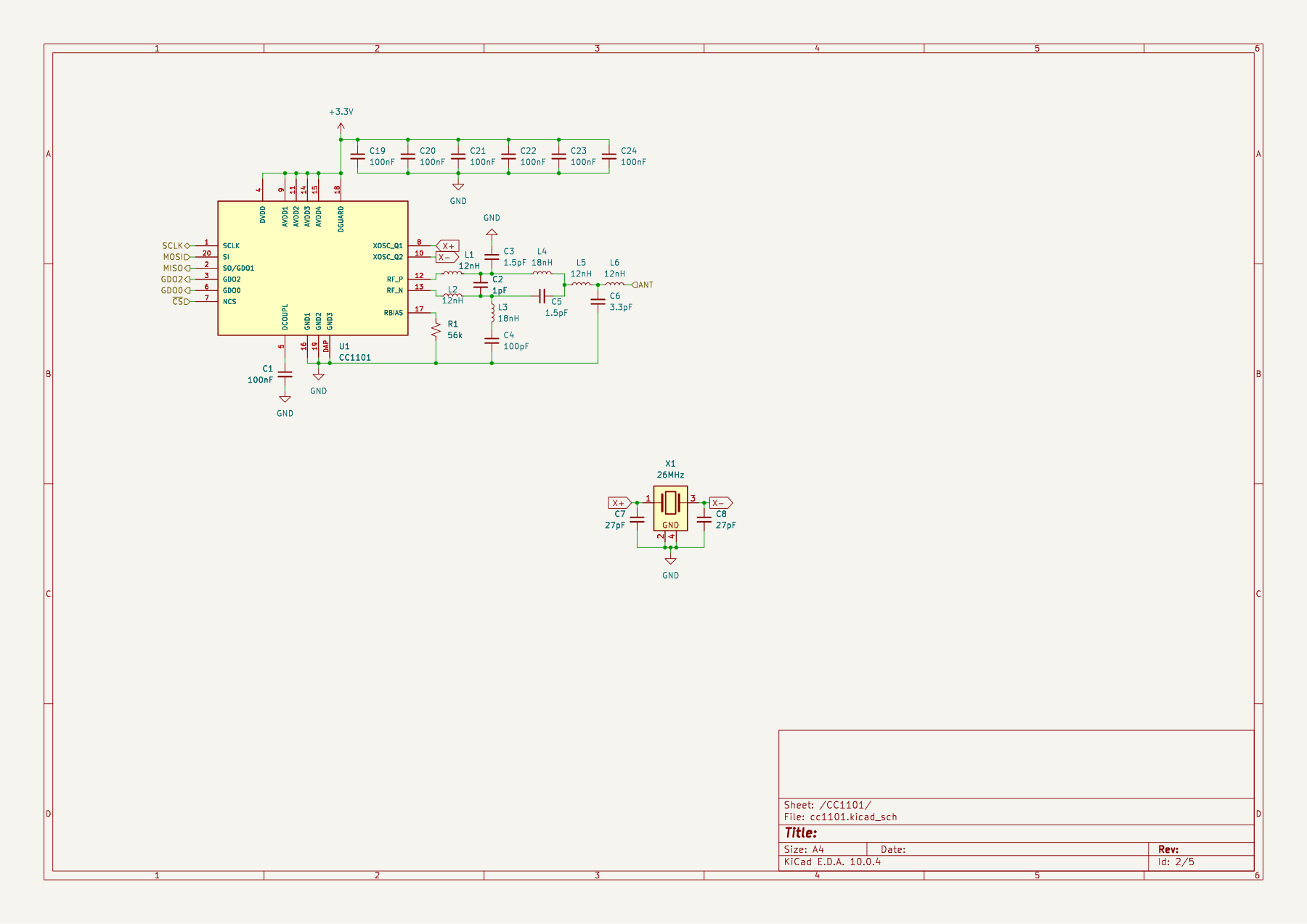
balun and match between CC1101, CC1190, and 50 ohm
Signal flow (TX): MCU -> SPI header -> CC1101 -> RF_P/RF_N -> balun and match -> CC1190 PA_IN -> CC1190 PA_OUT -> output match -> SMA -> antenna.
Signal flow (RX): antenna -> SMA -> RX match -> CC1190 LNA_IN -> LNA_OUT -> CC1101 -> SPI -> MCU.
GDO0 asserts PA_EN and GDO2 asserts LNA_EN. HGM is brought out to the header so the host can switch the CC1190 into high-gain mode with a GPIO or jumper.
PCB Design
Size: 55.54 x 33.86 mm.
Stackup: 4 layers, 1.6 mm, JLCPCB standard stackup (F.Cu / In1.Cu / In2.Cu / B.Cu).
Routing: Routed in KiCad 10, 208 track segments, 43 vias (0.6 mm diameter, 0.3 mm drill). No autorouter.
Track widths: 0.2 mm for signals, 0.35 mm for RF, 0.5 mm for power, 0.3 mm for short fanout.
Ground: continuous ground pour with stitching vias around the RF section and the two QFN exposed pads.
Layout: the CC1101, CC1190, matching network, and SMA are kept on the top side in a straight line so the RF path stays short. Decoupling capacitors sit next to the supply pins on each package.
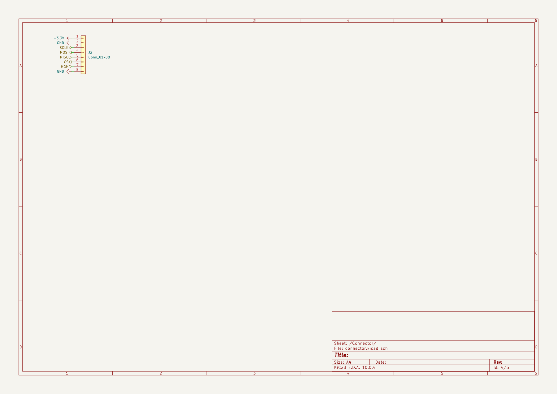
Schematic sheets, in reading order:
Firmware
None shipped - this is a passive module. It works with any SPI master that speaks the CC1101 protocol, for example the cc1101 Arduino library or register settings exported from TI SmartRF Studio. The two GDO lines are consumed by the on-board CC1190, so the host only needs MOSI, MISO, SCLK, CS, and optionally HGM for high gain mode.
Usage
Solder a 1x08 header to J2, or use the board as a soldered-down daughter card:
Pin
Function
1
+3.3 V (2.0-3.6 V)
2
GND
3
SCLK
4
MOSI
5
MISO
6
~CS
7
HGM (CC1190 high-gain mode, active high)
8
GND
Pull HGM high for maximum PA output, or tie it low for the default gain. Keep the supply clean and place a bulk capacitor near the header if the module is fed over a long cable.
BOM (Bill of Materials)
45 electrical parts plus two mechanical mounting holes.
Full BOM: BOM.csv
Item
Cost
Components, per board (45 parts)
$13.27
PCB, 4-layer, 5 pcs (estimate)
$10.00
Components for 5 boards
$66.35
Stencil (optional, for the QFN pads)
$10.00
Estimated total, 5 boards, no stencil, before shipping
$76.35
Shipping
varies
The edge-mount SMA is the single most expensive part at $8.56 each, so most of the component cost is the connector.
Production
Fabricated at JLCPCB: 4-layer, 1.6 mm, 1 oz copper, HASL, 55.54 x 33.86 mm.
Assembly data: kicad/production/bom.csv and kicad/production/positions.csv.
U1 and U2 are QFN packages with exposed pads - a stencil is recommended, and the center pads need to be reflowed properly.
J1 is an edge-mount SMA and may need hand soldering depending on the assembly house.
The board was routed by hand. If you re-spin it, keep the RF section short and do not autoroute it.
Repository Structure
text
CC1101_Module/
|-- kicad/                    # KiCad project, schematic, PCB, production files
|   |-- CC1101.kicad_pro
|   |-- CC1101.kicad_sch       # root schematic
|   |-- CC1101.kicad_pcb       # routed 4-layer board
|   |-- cc1101.kicad_sch       # CC1101 core sheet
|   |-- palna.kicad_sch        # CC1190 PA/LNA sheet
|   |-- sma.kicad_sch          # SMA and output match
|   |-- connector.kicad_sch    # 1x08 header
|   `-- production/            # gerbers, drill, BOM, positions
|-- parts/                     # custom symbols, footprints, 3D models
|-- cad/                       # STEP export of the assembled board
|-- blender/                   # PCB3D export for Blender
|-- images/                    # 3D renders, PCB plots, schematic exports
|-- BOM.csv                    # machine-readable BOM with links and total
|-- JOURNAL.md                 # build log
|-- README.md                  # this file
|-- LICENSE                    # CERN-OHL-P-2.0 (hardware)
`-- LICENSE-MIT                # MIT (docs and example code)
Known Issues
DRC is not clean yet. The current board reports 25 errors and 44 warnings: 7 clearance violations at 0.15-0.175 mm against a 0.2 mm project rule, 5 copper-to-edge violations at a board corner, 13 thermal-via drill-range errors (0.2 mm vias against a 0.3 mm rule), 43 silkscreen text-height warnings, and 1 library footprint mismatch. The clearance values are within JLCPCB's standard 4-layer capability, but the project rules should be reconciled before ordering.
The 27 pF crystal load capacitors come from the TI reference design. If the selected crystal trims to a lower load capacitance, they may need retuning on the bench.
The 0.5 pF and 8.2 pF matching values are from the TI CC1190 reference. Exact values may shift after real antenna tuning and should be checked with a VNA.
The edge-mount SMA is expensive and may require hand soldering.
No firmware examples are shipped, and the design has not been peer-reviewed or built yet.
The 4-layer stackup costs more than the 2-layer boards used in my other modules.
Credits & Inspiration
Texas Instruments CC1101 and CC1190 datasheets and reference designs - the matching network is derived from TI's CC1190 evaluation board.
KiCad, the open-source EDA suite.
LCSC and JLCPCB for parts and fabrication.
License
Hardware (schematic, PCB, footprints): CERN-OHL-P-2.0. See LICENSE.
An open-source, hacker-conference-style electronic badge built around the ESP32-S3-WROOM-1-N8R8 (8 MB flash + 8 MB Octal PSRAM), with swappable RF / audio / storage modules, an e-paper (or TFT) display socket, a secure…
190 parts17
Questions
How big is the CC1101 PCB?
It measures 50 × 30 mm and has 4 copper layers, 1.61 mm thick.
What parts does the CC1101 use?
47 parts, built around the CC1101RGP and CC1190. The full list of its parts is on this page, with links to each part's symbol and footprint where PCBKit's library has them.
Where can I download the CC1101 KiCad files?
From the sneakylizard123-4/CC1101_Module repository on GitHub, at the commit this page was made from: the board is kicad/CC1101.kicad_pcb and its schematic kicad/CC1101.kicad_sch. PCBKit opens the board in the browser, with nothing to install.
Can I use the CC1101 design in my own project?
Its repository publishes it under the CERN-OHL-P-2.0 licence: you may reuse it on that licence's terms (keep the author's notice, and for a copyleft licence share your changes alike).