Low-cost pothole detector: YOLOv8 + ESP32 + accelerometer. Logs a pothole only if the camera sees it AND the car feels it, with GPS & severity. Try it in Colab.
IPDS SensorNode is an open-source printed circuit board by SanTiwari07, from the SanTiwari07/PotHoleDetection repository on GitHub, published under the MIT licence. It is a 2-layer board of 117 × 68 mm with 14 parts on 42 nets, routed with 39 tracks and 11 vias.
It is built around the SS14. Its parts include 4 ICs, 2 capacitors, 2 resistors, 1 diode and 1 connector. It belongs with the home automation and IoT and radio and wireless boards and the ESP32 and RISC-V boards of this library.
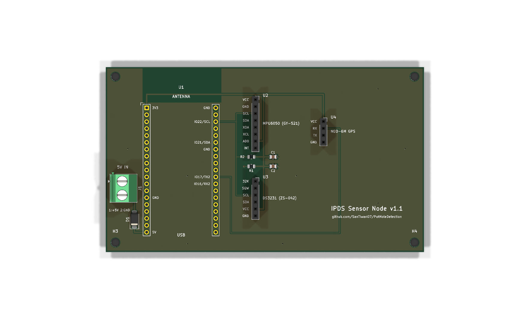
Carrier board for the IPDS sensor node: an ESP32-DevKitC (38-pin) plus plug-in MPU6050, DS3231 RTC and NEO-6M GPS breakout modules. Every module sits in a female header, so nothing is soldered to the modules themselves.
Board: 117 × 68 mm · 2 layers · 1.6 mm FR4 · GND pour on both sides · 4 × M3 mounting holes
Made with: KiCad 10.0 (open with KiCad 10 or newer)
AD0 is tied to 3V3 on this PCB, because 0x68 is already taken by the DS3231
The sensor firmware (ESP_32_Code/esp_32_final) uses exactly these pins and addresses. GPS UART runs at 9600 baud, 8N1.
Module pin order (match the silkscreen)
Socket
Module
Pin order (pin 1 = square pad, top)
U2 (1×8)
GY-521 MPU6050
VCC, GND, SCL, SDA, XDA, XCL, AD0, INT
U3 (1×6)
ZS-042 DS3231
32K, SQW, SCL, SDA, VCC, GND
U4 (1×4)
GY-NEO6MV2
VCC, RX, TX, GND
Breakout boards from different sellers sometimes order their pins differently. Check your module's printed labels against the table before plugging it in.
Before you order
Measure your ESP32 board. The footprint expects the two pin rows 25.4 mm (1.0") apart, as on Espressif's DevKitC V4 and most 38-pin clones. Some "narrow" clones are 22.86 mm; if yours is, move the right-hand row in IPDS.pretty.
Power: feed 5 V into J1 (e.g. a car USB adapter) or use the DevKit's USB port. If your DevKit has no diode on its USB 5 V line, don't connect both at once: D1 stops J1 from being back-fed, but USB could be back-fed from J1.
ZS-042 with a CR2032: the module has a charging circuit meant for rechargeable LIR2032 cells. With a normal CR2032, remove its 200 Ω resistor (or the diode next to it).
Bill of materials
Qty
Ref
Part
Notes
1
U1
ESP32-DevKitC 38-pin
plus 2 × 1×19 female headers, 2.54 mm
1
U2
GY-521 MPU6050 module
1×8 female header
1
U3
ZS-042 DS3231 module + CR2032
1×6 female header
1
U4
GY-NEO6MV2 NEO-6M GPS module + antenna
1×4 female header
1
J1
Phoenix MKDS 1,5/2-5.08 screw terminal
or any 5.08 mm 2-pin terminal
1
D1
SS14 Schottky diode, SMA
1 A, 40 V
2
R1, R2
4.7 kΩ, 0805
I²C pull-ups
1
C1
100 nF, 0805
decoupling
1
C2
10 µF, 0805, ≥10 V
bulk
4
—
M3 standoffs + screws
mounting
Ordering the PCB
Upload fabrication/IPDS_SensorNode_gerbers.zip to JLCPCB, PCBWay or a similar fab with the defaults: 2 layers, 1.6 mm, HASL, 1 oz copper. All tracks are ≥ 0.25 mm and clearances ≥ 0.2 mm, so standard (cheapest) capabilities are enough.
To regenerate the outputs after editing: File → Fabrication Outputs → Gerbers and Drill Files in the PCB editor, after re-running Inspect → Design Rules Checker.
It measures 117 × 68 mm and has 2 copper layers, 1.6 mm thick.
What parts does the IPDS SensorNode use?
14 parts, built around the SS14. The full list of its parts is on this page, with links to each part's symbol and footprint where PCBKit's library has them.
Where can I download the IPDS SensorNode KiCad files?
From the SanTiwari07/PotHoleDetection repository on GitHub, at the commit this page was made from: the board is KiCad/IPDS_SensorNode/IPDS_SensorNode.kicad_pcb and its schematic KiCad/IPDS_SensorNode/IPDS_SensorNode.kicad_sch. PCBKit opens the board in the browser, with nothing to install.
Can I use the IPDS SensorNode design in my own project?
Its repository publishes it under the MIT licence: you may reuse it on that licence's terms (keep the author's notice, and for a copyleft licence share your changes alike).
The Smart Plant is a board that can be plugged directly on the soil, close to the plant, that allows the measurement of the environment (soil moisture, environment temperature & illuminance), and presents the…
Drone Show Software is software designed for drone shows, allowing flight path planning as well as control of dozens of drones simultaneously in a synchronized manner.