6 layers81.5 × 50 mm
Picard
weiiwang01/picard
PiCard is a miniaturized Raspberry Pi Compute Module carrier board optimized for Linux server use cases.
166 parts8

 protolux-electronics/trellis_core13
A barebones KiCad project for Allwinner T113-based designs
Trellis core is an open-source printed circuit board by protolux-electronics, from the protolux-electronics/trellis_core repository on GitHub, published under the CERN-OHL-P-2.0 licence. It is a 4-layer board of 50 × 50 mm with 89 parts on 126 nets, routed with 528 tracks and 80 vias.
It is built around the T113M4020DC0, TLV62569PDDCR and ZDSD04GLGEAG, with the SN74AHC1G08DCKR, USBLC6-2SC6 and CL05B104KB54PNC among its other parts. Its parts include 44 capacitors, 25 resistors, 6 ICs, 2 switches and 2 inductors. It belongs with the computers and single-board computers boards of this library.


This repo serves as a minimum hardware design for the Allwinner T113-S4 (part number sometimes referred to as T113M4020). This is pin-compatible with the T113-S3, but with 256MB of RAM in-package. Although generally software-agnostic, this repo is designed to be used with Nerves and nerves_system_trellis.
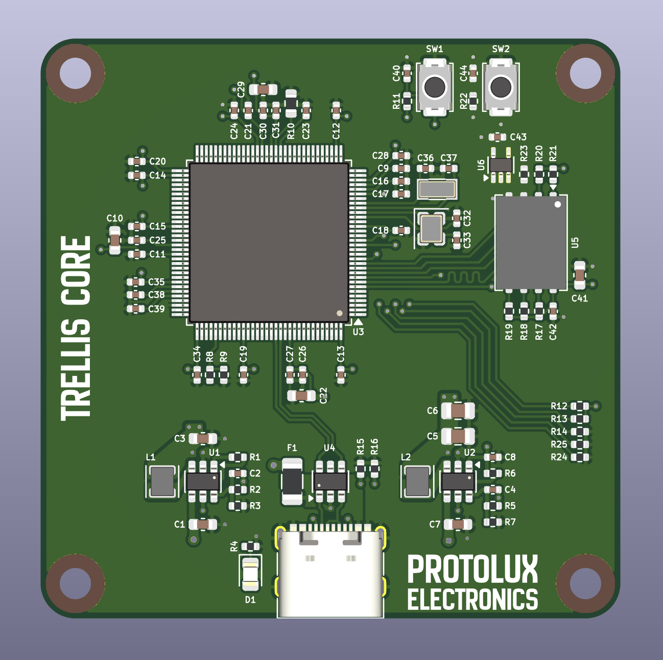
[!NOTE] This hardware design has been extracted out of several proven designs that I have previously ordered and tested. While the schematic should be sufficient to minimally bring up Linux on this board, the routing and layout as is available in this repo has not been tested. You will almost certainly need to change it for your application. See the suggestions below.
Want to view the schematic and layout in your browser? Paste this repo's URL into KiCanvas by @theacodes.
KiCad version 9 or later is required to modify these
designs. To get started, clone this repo and open trellis_core.kicad_pro (you
may rename all trellis_core.kicad_* files first, if desired). The schematic
already includes:
To add your required peripherals, connect the appropriate signals in the
CPU IO sheet. You can see the GPIO pin multiplexing capabilities for the chip
on page 30 of the
T113 datasheet
The routing shown in the example board was done rather quickly to showcase the basics of routing a PCB, while also showing best practices. It uses pretty standard and inexpensive processes - including 0.2mm minimum trace size, 0.3mm via drill diameter, and 0402 components. Part numbers have been included in the metadata for each component, and parts were chosen to maximize the use of basic and preferred components with JLC assembly.
The board uses a standard 4-layer stackup, with the following layers:
| Layer | Type |
|---|---|
| Top | Signal + GND |
| In1 | GND Plane |
| In2 | 3.3V Plane |
| Bottom | Signal + GND |
For the USB trace, 90 Ohm impedance is required. The trace width and spacing was calculated for the JLC04161H-7628 stackup from JLCPCB, using the JLCPCB impedance calculator. Different manufacturers or stackups may require different settings - please double check before ordering.
Finally, this design only populates components on the top side to reduce assembly complexity and cost.
As mentioned above, this exact design has not been ordered and tested (derivatives have been, though). If you use this as the template for your project, I suggest making the following changes to the routing:
Copyright 2025 by Protolux Electronics SARL-S
Trellis Core hardware design files are released under the CERN Open Hardware Licence, Permissive (CERN-OHL-P). See the LICENSE file for the complete legal text. In summary:
This is a permissive open hardware license, and is similar in spirit to MIT or BSD licenses in software. It encourages reuse, even in commercial contexts, while preserving proper attribution.
[!NOTE] Some 3D component models and other assets in this repository are provided under their original authors’ licenses. Refer to the individual files or their directories for details.
Disclaimer: The Trellis Core design is provided "as is", without any warranty or guarantee of performance. Use, manufacture, or modification of this hardware is entirely at your own risk.
The Protolux Electronics name and logo are trademarks of Protolux Electronics SARL-S.
These marks are not licensed under the CERN-OHL-P license. You may not use the Protolux Electronics logo or trademarks on any modified versions of this hardware, on derivative products, or in any way that suggests endorsement or origin from Protolux Electronics, unless you have received prior written permission.
Feel free to open a PR to add your project here! These are some existing projects that are based off of this design:
| Name | Author | Description |
|---|---|---|
| Wisteria | Protolux Electronics/Gus Workman | Wisteria is the hardware for the 2025 Goatmire e-ink name badge. Read more about it here |
| Trellis Dev Kit | Protolux Electronics/Gus Workman | WIP! Check back soon :) |
| Nerves Getting Started Hardware Kit [blocked] | Protolux Electronics/Gus Workman | WIP! Check back soon :) |
| Your board here | You | Share your design - open a PR! |
Need help with your next embedded project? Interested in a customized T113-based Nerves board? We're Protolux Electronics, a Luxembourg-based consultancy that provides hardware and embedded software design services, as well as manufacturing support. We specialize in embedded solutions using Nerves and Elixir. Check us out at https://protolux.io
| Qty | Value | Footprint | References |
|---|---|---|---|
| 25 | 100n | Capacitor_SMD:C_0402_1005Metric | C11, C12, C13, C14, C15, C17, C18, C19, C20, C21, C23, C24, C25, C26, C27, C30 +9 |
| 9 | 5k1 | Resistor_SMD:R_0402_1005Metric | R4, R12, R13, R14, R15, R16, R22, R24, R25 |
| 7 | 10u | Capacitor_SMD:C_0603_1608Metric | C1, C3, C7, C10, C22, C29, C41 |
| 6 | 51k | Resistor_SMD:R_0402_1005Metric | R5, R17, R18, R19, R20, R21 |
| 5 | 100k | Resistor_SMD:R_0402_1005Metric | R1, R3, R6, R7, R11 |
| 4 | 10p | Capacitor_SMD:C_0402_1005Metric | C2, C4, C32, C33 |
| 4 | 2u2 | Capacitor_SMD:C_0402_1005Metric | C9, C16, C28, C40 |
| 4 | MountingHole_2.7mm_M2.5_DIN965 | MountingHole:MountingHole_2.7mm_M2.5_DIN965 | H1, H2, H3, H4 |
| 2 | 18p | Capacitor_SMD:C_0402_1005Metric | C36, C37 |
| 2 | 22u | Capacitor_SMD:C_0805_2012Metric | C5, C6 |
| 2 | 2u2 | Inductor_SMD:L_Wuerth_MAPI-2510 | L1, L2 |
| 2 | SW_Push | Button_Switch_SMD:SW_Push_SPST_NO_Alps_SKRK | SW1, SW2 |
| 2 | TLV62569PDDCR | Package_TO_SOT_SMD:SOT-23-6 | U1, U2 |
| 2 | TODO | Resistor_SMD:R_0402_1005Metric | R8, R9 |
| 1 | 1A | Fuse:Fuse_1206_3216Metric | F1 |
| 1 | 22R | Resistor_SMD:R_0402_1005Metric | R23 |
| 1 | 240R | Resistor_SMD:R_0603_1608Metric | R10 |
| 1 | 24MHz | Crystal:Crystal_SMD_2520-4Pin_2.5x2.0mm | Y1 |
| 1 | 32.768kHz | Crystal:Crystal_SMD_3215-2Pin_3.2x1.5mm | Y2 |
| 1 | 453k | Resistor_SMD:R_0402_1005Metric | R2 |
| 1 | G*** | kibuzzard-68FD2BE5 | kibuzzard-68FD2BE5 |
| 1 | RED | LED_SMD:LED_0805_2012Metric | D1 |
| 1 | SN74AHC1G08 | Package_TO_SOT_SMD:Texas_R-PDSO-G5_DCK-5 | U6 |
| 1 | T113-S3 | gworkman_mpu:T113-S3 | U3 |
| 1 | USBLC6-2SC6 | Package_TO_SOT_SMD:SOT-23-6 | U4 |
| 1 | USB_C_Receptacle_USB2.0_14P | Connector_USB:USB_C_Receptacle_G-Switch_GT-USB-7010ASV | J1 |
| 1 | ZDSD08GLGEAG | Package_LGA:LGA-8_8x6mm_P1.27mm | U5 |
weiiwang01/picard
PiCard is a miniaturized Raspberry Pi Compute Module carrier board optimized for Linux server use cases.

sedlak477/owl-hardware
Hardware design files and build instructions for the OWL platform

TheKingOfChaos/RF-Power-Monitor
A 2-layer carrier board for the WIZnet W5500-EVB-Pico-PoE. It is 80 x 51.5 mm: exactly as long as the module, so both short edges line up with the module.


danieltyukov/owltunes
Owl-shaped Spotify remote for your desk and pocket: ESP32-S3 firmware, LVGL UI, KiCad PCB, 3D-printed enclosure, and owl v0 on the Waveshare AMOLED kit


marcoallegretti/Teresina-Rack
The goal is an open, self-fabricatable Daisy Patch SM-compatible Eurorack submodule: the same carrier interface and libDaisy application compatibility through a small Teresina firmware variant.

usr-ein/TriMixxx
Open source standalone DJ multimedia player, compatible with Rekordbox
It measures 50 × 50 mm and has 4 copper layers, 1.6 mm thick.
89 parts, built around the T113M4020DC0, TLV62569PDDCR, ZDSD04GLGEAG and SN74AHC1G08DCKR. The full list of its parts is on this page, with links to each part's symbol and footprint where PCBKit's library has them.
From the protolux-electronics/trellis_core repository on GitHub, at the commit this page was made from: the board is src/trellis_core.kicad_pcb and its schematic src/architecture.kicad_sch. PCBKit opens the board in the browser, with nothing to install.
Its repository publishes it under the CERN-OHL-P-2.0 licence: you may reuse it on that licence's terms (keep the author's notice, and for a copyleft licence share your changes alike).