
4 layers53.7 × 21 mm
Pico WH
sabogalc/project-piCo
Because it should be a crime to release a product with Micro-USB in the 2020s
93 parts159WTFPL

 mikeysklar/pi-debug-swd-adapter
Passive adapter: Raspberry Pi Debug Probe (JST-SH 3-pin) to standard 2x5 1.27mm ARM Cortex SWD header. Single-sided, home-etched.
Pico debug swd adapter is an open-source printed circuit board by mikeysklar, from the mikeysklar/pi-debug-swd-adapter repository on GitHub, published under the GPL-3.0 licence. It is a 2-layer board of 26.6 × 11 mm with 2 parts on 9 nets, routed with 10 tracks and 0 vias.
It is built around the BM03B-SRSS-TB. It belongs with the interfaces and adapters and sensors and measurement boards and the RP2040 boards of this library.
Connects the $12 Raspberry Pi Debug Probe to a standard 2x5 SWD connector.
Voice dictated to Claude, which sourced the parts and wrote out the KiCad schematic and PCB board file. No MCP server, no skill, no reference design.
See CLAUDE.md for what it was used. This file represents the on-going changes I had Claude
make after the first pass.
Fabrication: a Bantam CNC to cut the single sided PCB blanks, and an xTool F1 Ultra fiber laser to etch, silkscreen, and expose the pads under a green resin layer was applied. The steel business card stencil was cut on the same laser.
The Raspberry Pi Debug Probe ends in a 3-pin JST-SH connector. Many Adafruit Metro and Feather boards expose debug on the standard 2x5 1.27 mm SWD header. This board bridges the two.
No active parts — just three signals and a ground pour on a 26.6 × 11 mm single-sided board.
Design files are in kicad/.
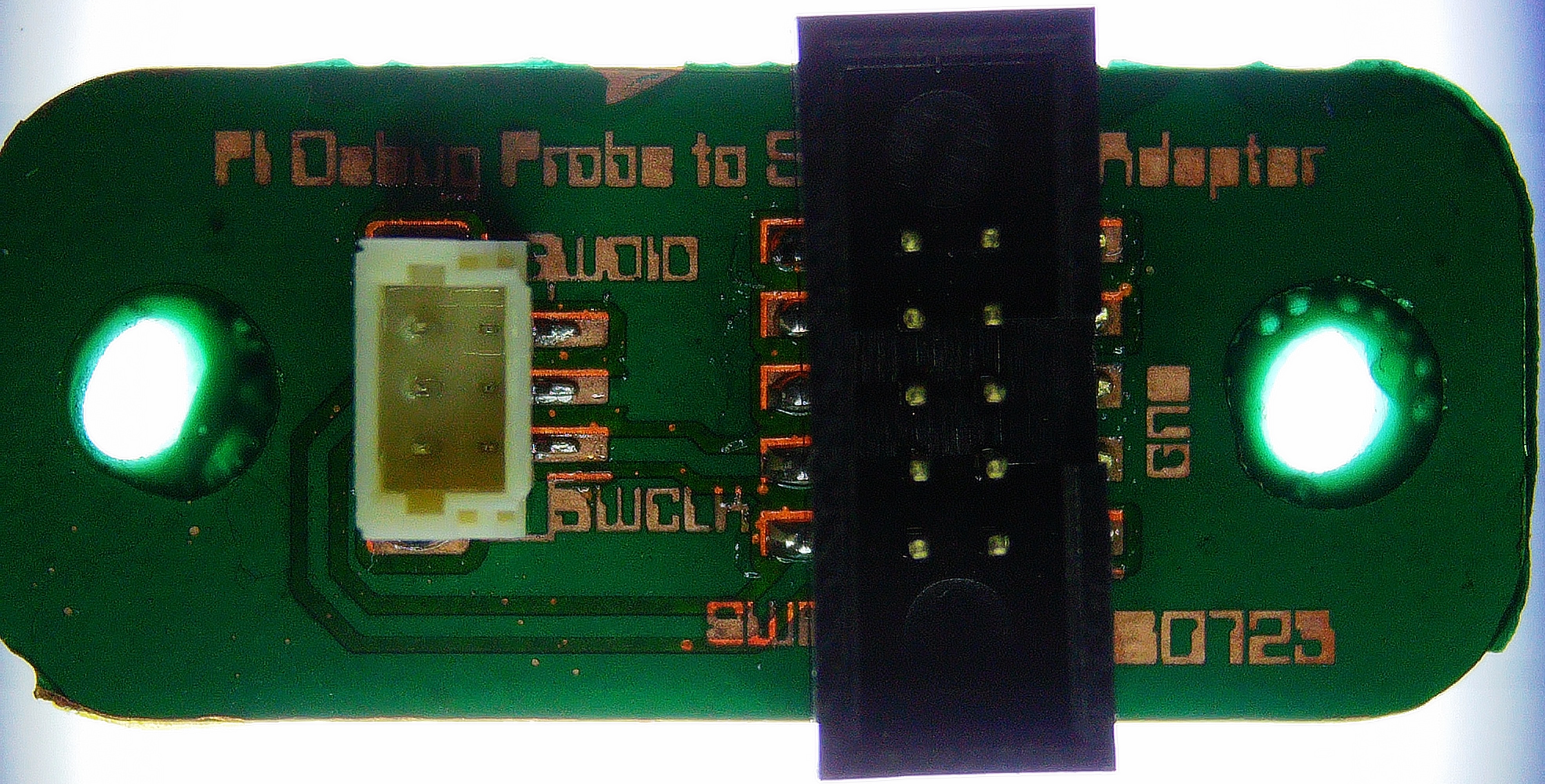
The finished prototype, backlit. Both connectors reflowed onto the laser-exposed pads, with the copper silkscreen and board name still readable through the green resin.
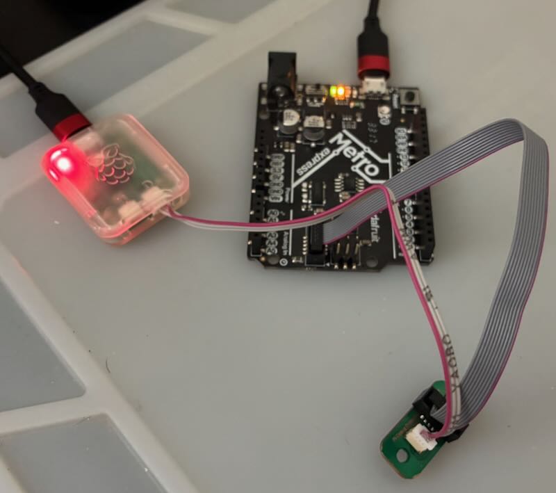
The whole chain in use: Debug Probe on the left, its 3-pin JST-SH lead into the adapter at bottom right, and a 2x5 1.27 mm ribbon up to the SWD header on an Adafruit Metro M0 Express.
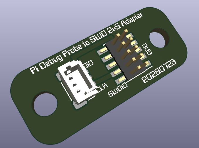
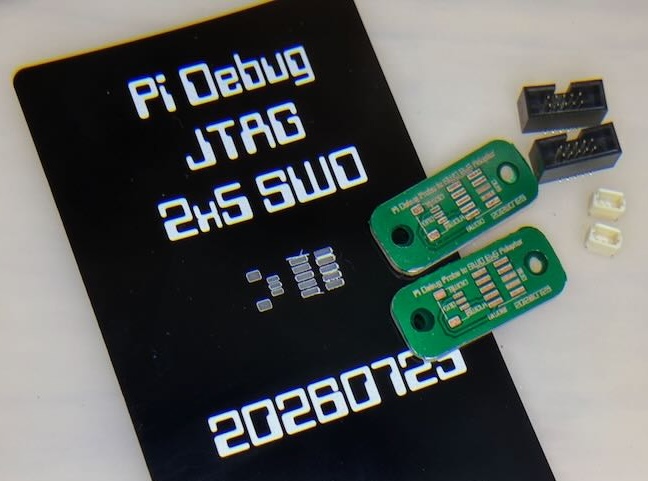
What the board was supposed to look like before any copper got cut.
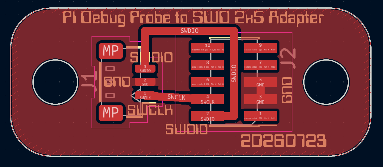
The original layout, and the oldest artifact here. The board name is set in copper so it etches as readable text.
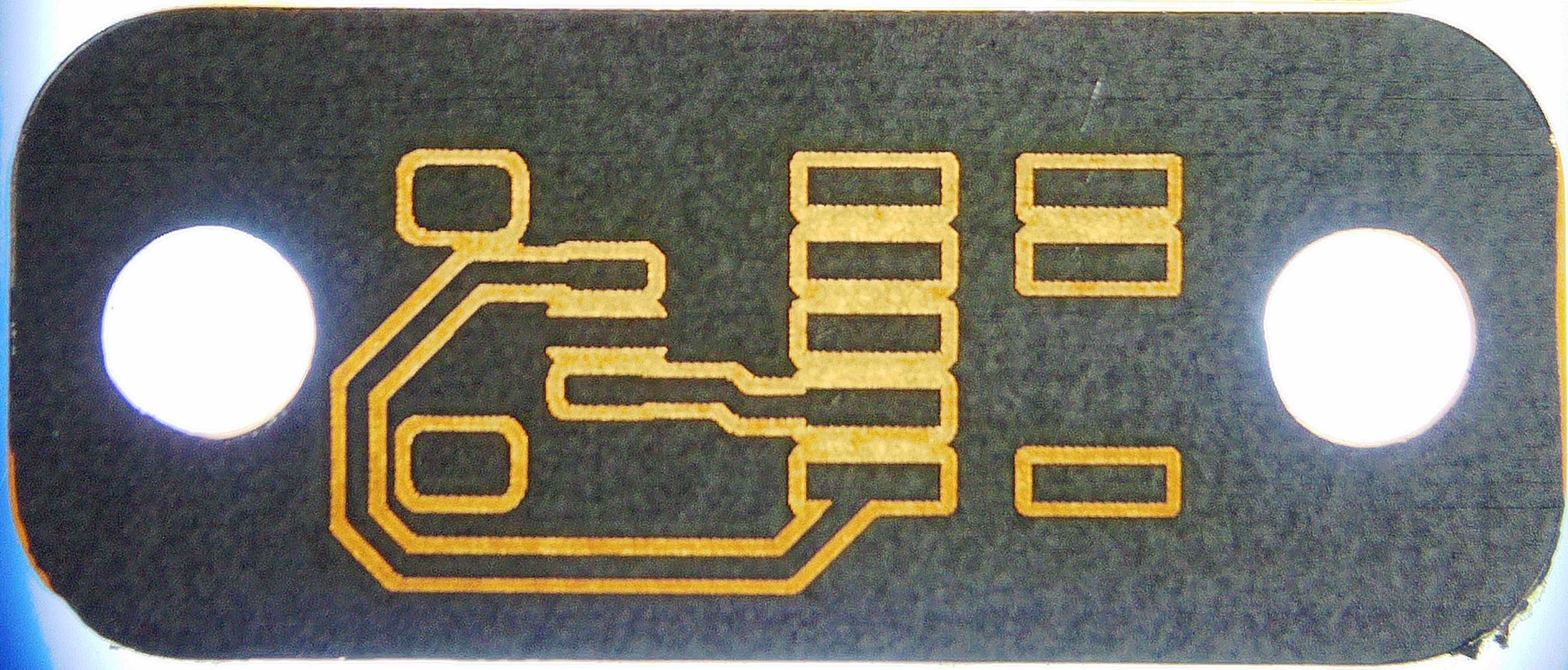
A freshly etched board held up to a light to check the traces. All copper is on one side — no vias.
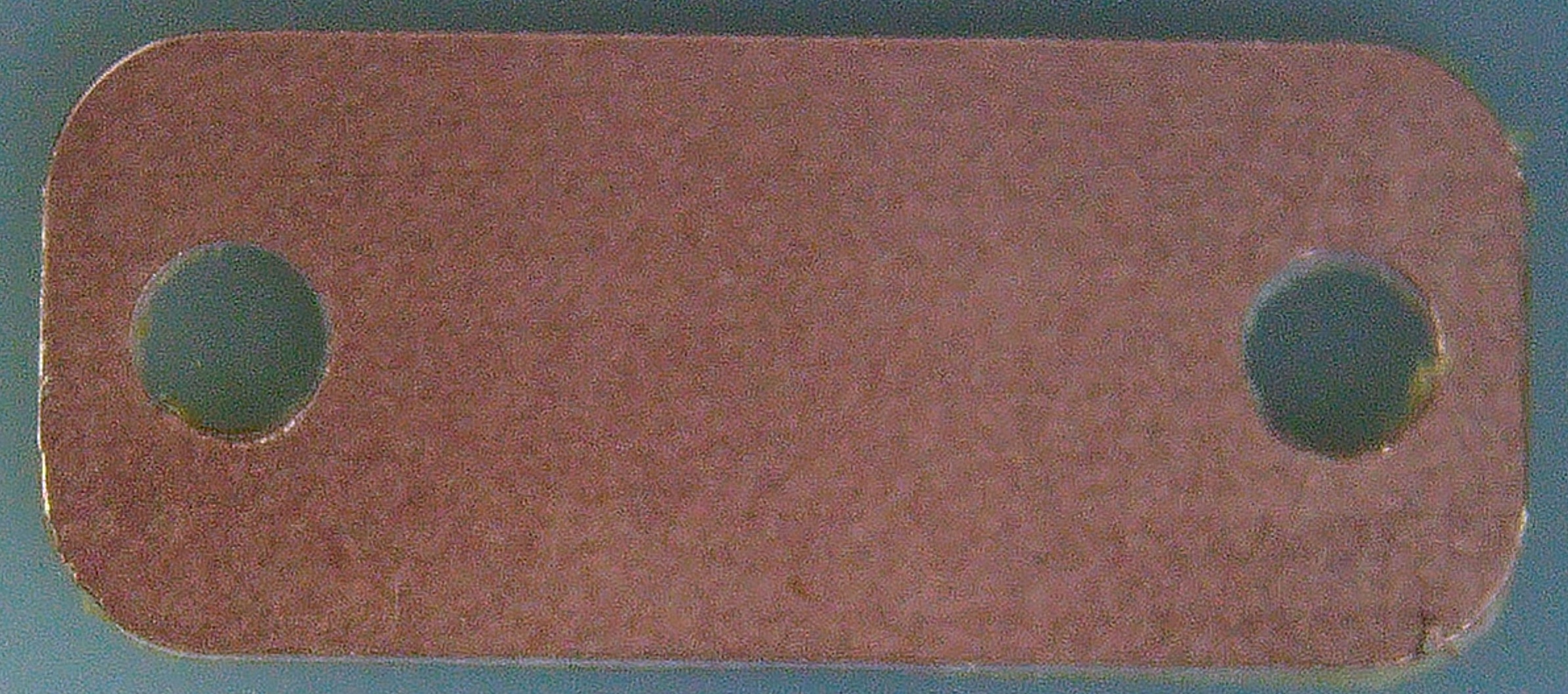
The raw blank milled on the Bantam CNC, with rounded corners and two M2.5 mounting holes.
Designed in KiCad 9. The project lives in kicad/:
pico-debug-swd-adapter.kicad_pro — project filepico-debug-swd-adapter.kicad_sch — schematicpico-debug-swd-adapter.kicad_pcb — PCB layoutpico-debug-swd-adapter.step — 3D model exportpi-debug-swd_recovered.xcs — xTool Creative Space laser job3dmodels/ — project-local STEP modelsetch/etch-FCu-MIRRORED-1to1.pdf — print at 100% for toner transferetch/etch-FCu-reference.pdf — same artwork unmirrored, for checking| Ref | Part | Description |
|---|---|---|
| J1 | JST BM03B-SRSS-TB | 3-pin 1.00 mm vertical SMT receptacle |
| J2 | CNC Tech 3220-10-0300-00 | 2x5 1.27 mm shrouded SWD box header, SMT |
Plus two M2.5 screws and a 2x5 1.27 mm ribbon cable.
| Debug Probe "D" (J1) | Cortex Debug 2x5 (J2) |
|---|---|
| 1 — SC | 4 — SWCLK |
| 2 — GND | 3, 5 — GND |
| 3 — SD | 2 — SWDIO |
Everything else on J2 is left unconnected. Use the "D" port on the probe, not "U".
The Debug Probe shows up as CMSIS-DAP, so no special driver is needed. Connecting to the Adafruit Metro M0 Express in the photo above, through this adapter:
$ openocd -f interface/cmsis-dap.cfg -f target/at91samdXX.cfg \
    -c "adapter speed 400" -c "init; reset halt; flash probe 0; targets; shutdown"

Open On-Chip Debugger 0.12.0
adapter speed: 400 kHz

Info : Using CMSIS-DAPv2 interface with VID:PID=0x2e8a:0x000c, serial=E6614103E7687D25
Info : CMSIS-DAP: SWD supported
Info : CMSIS-DAP: FW Version = 2.0.0
Info : CMSIS-DAP: Interface Initialised (SWD)
Info : CMSIS-DAP: Interface ready
Info : clock speed 400 kHz
Info : SWD DPIDR 0x0bc11477
Info : [at91samd.cpu] Cortex-M0+ r0p1 processor detected
Info : [at91samd.cpu] target has 4 breakpoints, 2 watchpoints
Info : starting gdb server for at91samd.cpu on 3333
Info : Listening on port 3333 for gdb connections
[at91samd.cpu] halted due to debug-request, current mode: Thread
xPSR: 0x71000000 pc: 0x00000264 msp: 0x20002de0
Info : SAMD MCU: SAMD21G18A (256KB Flash, 32KB RAM)
shutdown command invoked
SWD DPIDR 0x0bc11477 is the handshake landing. After that the probe halts the core and
reads the chip back as a SAMD21G18A, which is the part on the Metro M0.
The Debug Probe does not power the target, so bring the target up on its own supply and leave
it powered before starting OpenOCD. A target that is off gives
Error: Error connecting DP: cannot read IDR.
| Qty | Value | Footprint | References |
|---|---|---|---|
| 1 | 3220-10-0300-00 | PinHeader_2x05_P1.27mm_Vertical_SMD | J2 |
| 1 | BM03B-SRSS-TB | JST_SH_BM03B-SRSS-TB_1x03-1MP_P1.00mm_Vertical | J1 |
sabogalc/project-piCo
Because it should be a crime to release a product with Micro-USB in the 2020s

tinyvision-ai-inc/pico2-ice
Doc | Hardware | SDK | Schematic | Assembly | Discord

ErichStyger/McuLink-Mini
Version of the NXP MCU-Link Debug CMSIS-DAP Debug Probe.

smartbank-inc/Board43
Board43 is an RP2350A-based microcontroller development board. Flash PicoRuby or your favorite firmware and start hacking.


It measures 26.6 × 11 mm and has 2 copper layers, 1.6 mm thick.
2 parts, built around the BM03B-SRSS-TB. The full list of its parts is on this page, with links to each part's symbol and footprint where PCBKit's library has them.
From the mikeysklar/pi-debug-swd-adapter repository on GitHub, at the commit this page was made from: the board is kicad/pico-debug-swd-adapter.kicad_pcb and its schematic kicad/pico-debug-swd-adapter.kicad_sch. PCBKit opens the board in the browser, with nothing to install.
Its repository publishes it under the GPL-3.0 licence: you may reuse it on that licence's terms (keep the author's notice, and for a copyleft licence share your changes alike).