4 layers40 × 65 mm
P-1000101 Cicada WiSun
EnAccess/Cicada-WiSUN-HW
IoT Communications Module for Energy Access. A quick way to get production ready, bi-directional communications for your IoT embedded device.
118 parts

 Mehdi-Ldj/lora-ble-sensor-node
Off-grid LoRa/BLE sensor node — 868 MHz LoRa, 2.4 GHz BLE, solar/LiFePO4
Lora node is an open-source printed circuit board by Mehdi-Ldj, from the Mehdi-Ldj/lora-ble-sensor-node repository on GitHub, published under the CERN-OHL-P-2.0 licence. It is a 4-layer board with 110 parts on 107 nets, routed with 674 tracks and 200 vias.
It is built around the SX1262IMLTRT, NRF52840-QIAA-R and BME280, with the TPS61099DRV, BQ25570RGRR and CL21A106KAYNNNE among its other parts. Its parts include 48 capacitors, 15 resistors, 12 inductors, 6 connectors and 5 ICs. It belongs with the radio and wireless and home automation and IoT boards and the nRF52 and nRF5x boards of this library.


A 55 mm round, four-layer sensor node that runs from a solar cell and a 14500 LiFePO4 cell: 868 MHz LoRa, 2.4 GHz BLE, and an environmental sensor suite on one board.
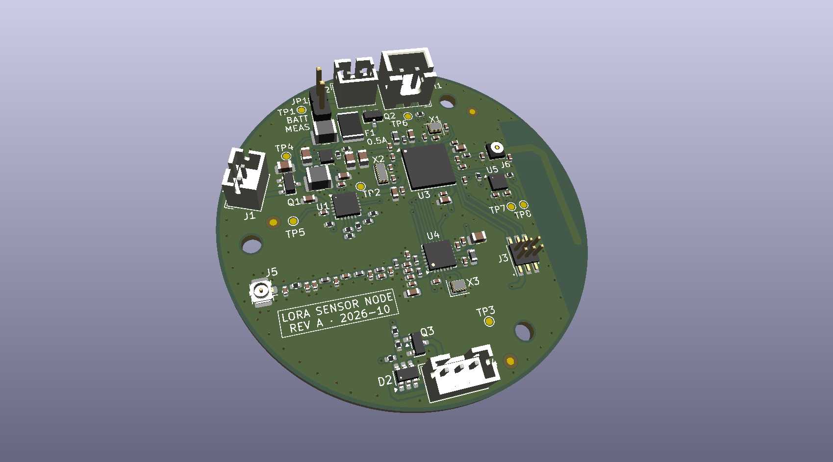
| Schematic | Board |
|---|---|
| Schematic, six pages (PDF) | Open the project in KiCanvas |
KiCanvas loads the whole project in the browser: the board opens first, and the five sheets are one click away in its Project panel. No KiCad installation required. The PDF is the quickest way to read the schematic end to end.
The node is meant to sit in a field and report microclimate data for months at a time without a battery change. A solar harvester tops up a single LiFePO4 cell, a boost holds 3.3 V, and the MCU wakes to sample temperature, humidity and soil moisture before transmitting over LoRa.
Three choices shaped the board more than anything else:
The outline is the last constraint: Ø55 mm, three mounting holes, and an antenna keepout that no layer may cross.
| Item | Value |
|---|---|
| Board size | Ø 55.0 mm, 4 layers |
| Stackup | JLC04161H-7628, FR4, Er 4.6, 1.6 mm nominal |
| Copper | 1 oz outer and inner, ENIG finish, green mask, white silk |
| Minimum feature | 0.20 mm track, 0.15 mm clearance, 0.20 mm drill |
| Vias | 0.30/0.20 mm and 0.20/0.20 mm, tented, no blind or buried |
| Impedance | 50 Ω ±10 % single-ended, In1.Cu reference |
| Assembly | JLCPCB Standard PCBA, 2 prototypes |
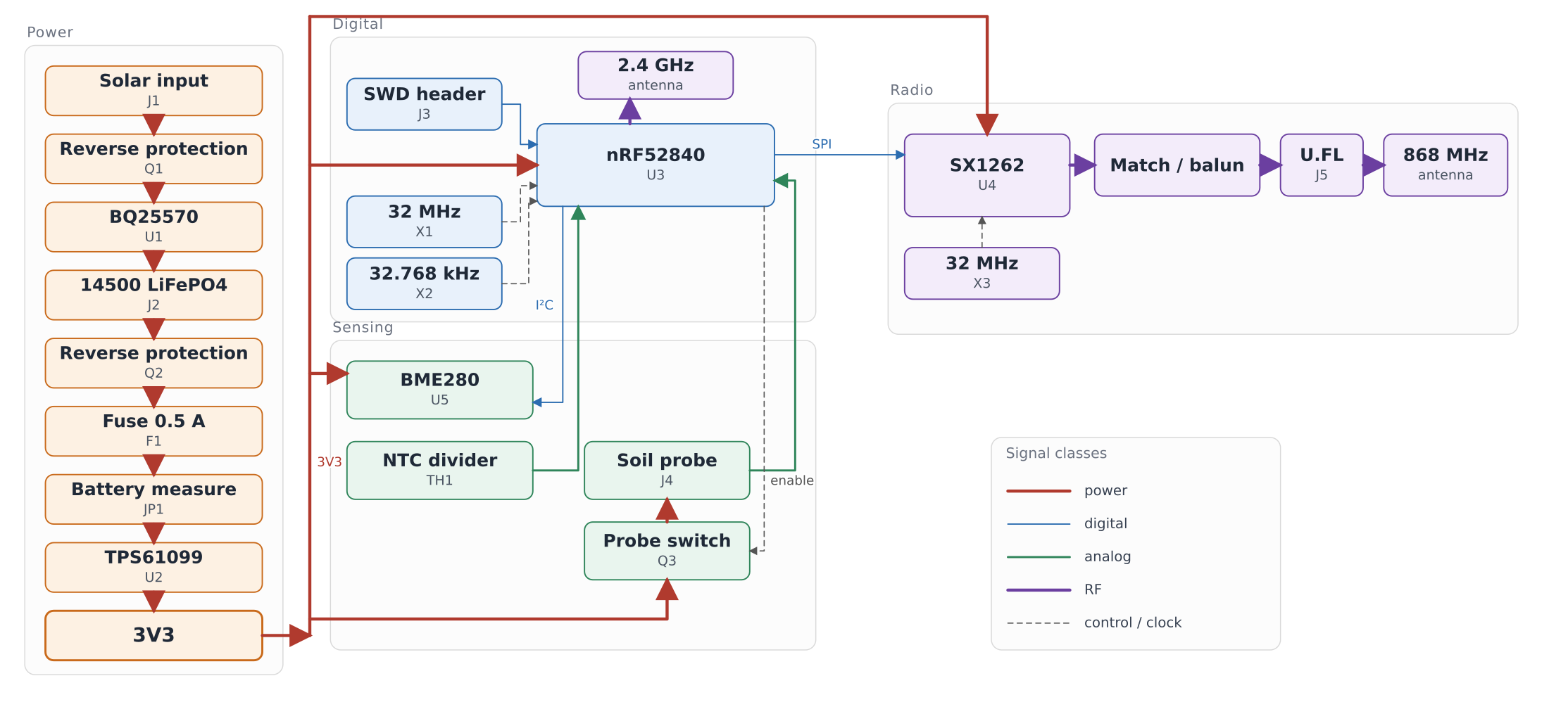
Line colour and weight separate the five signal classes: power, digital, analog, RF and control. The 3V3 bus feeds the radio and the sensing block from the same boost converter, and the soil probe is switched so it draws nothing while the node sleeps.
The radio sheet carries a switchless match, filter and balun between the SX1262 and the U.FL, laid out as a 50 Ω coplanar waveguide over the In1.Cu ground plane. The geometry was chosen from a quasi-static 2D sweep before layout:
| W (mm) | S (mm) | h (mm) | Z₀ (Ω) | εeff |
|---|---|---|---|---|
| 0.38 | 0.20 | 0.210 | 50.4 | 3.51 |
The sweep and its caveats are in
simulation/results/cpw_sweep.md. The
full-wave model and the VNA coupon are still to be run.
The PCB antenna sits in a keepout with no copper on any layer, fed from the
nRF52840 through the same 50 Ω class. The keepout is the fragile part, and it is
documented with the stackup in docs/stackup.md.
The BQ25570 runs as a boost charger only — its buck converter is deliberately unused — feeding a single LiFePO4 cell through a PTC and a reverse-polarity PMOS. The TPS61099 then holds 3.3 V for the MCU, radio and sensors, and the soil probe is switched so it cannot leak current while the node sleeps. The full pin list and the reviewed net table are in the schematic.
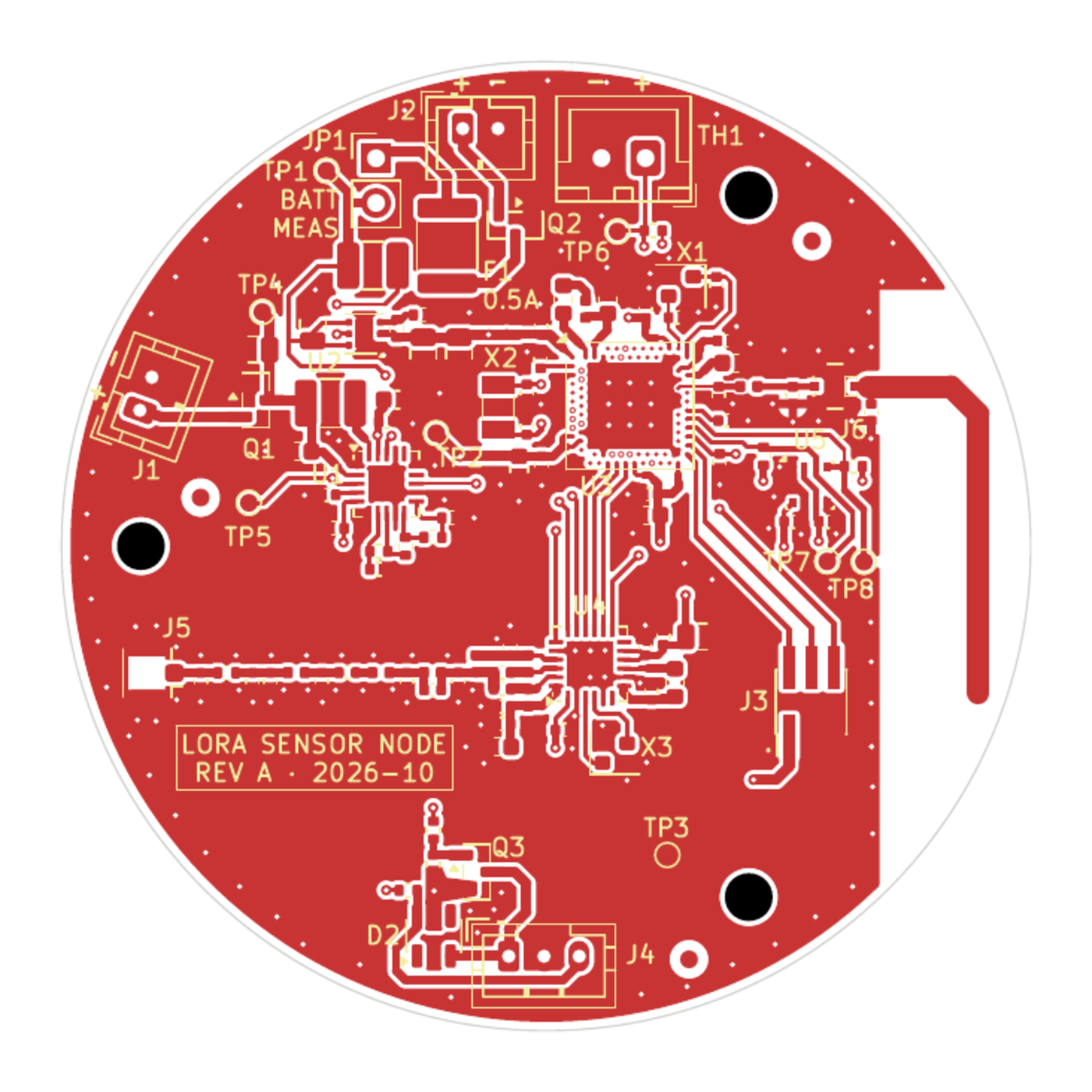
Four layers carry the aQFN73 fanout on the top, a solid ground below it, and the supplies on the inner layers. Assembly is Standard PCBA with X-ray, because the aQFN73 and the BME280 both have pads underneath.
| Front copper | Back copper |
|---|---|
 | 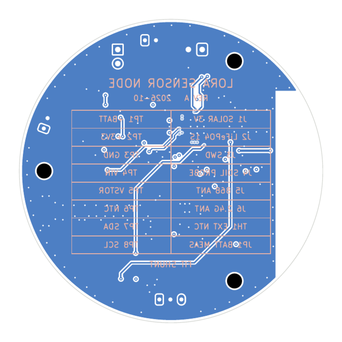 |
| Inner 1 — ground plane | Inner 2 — power |
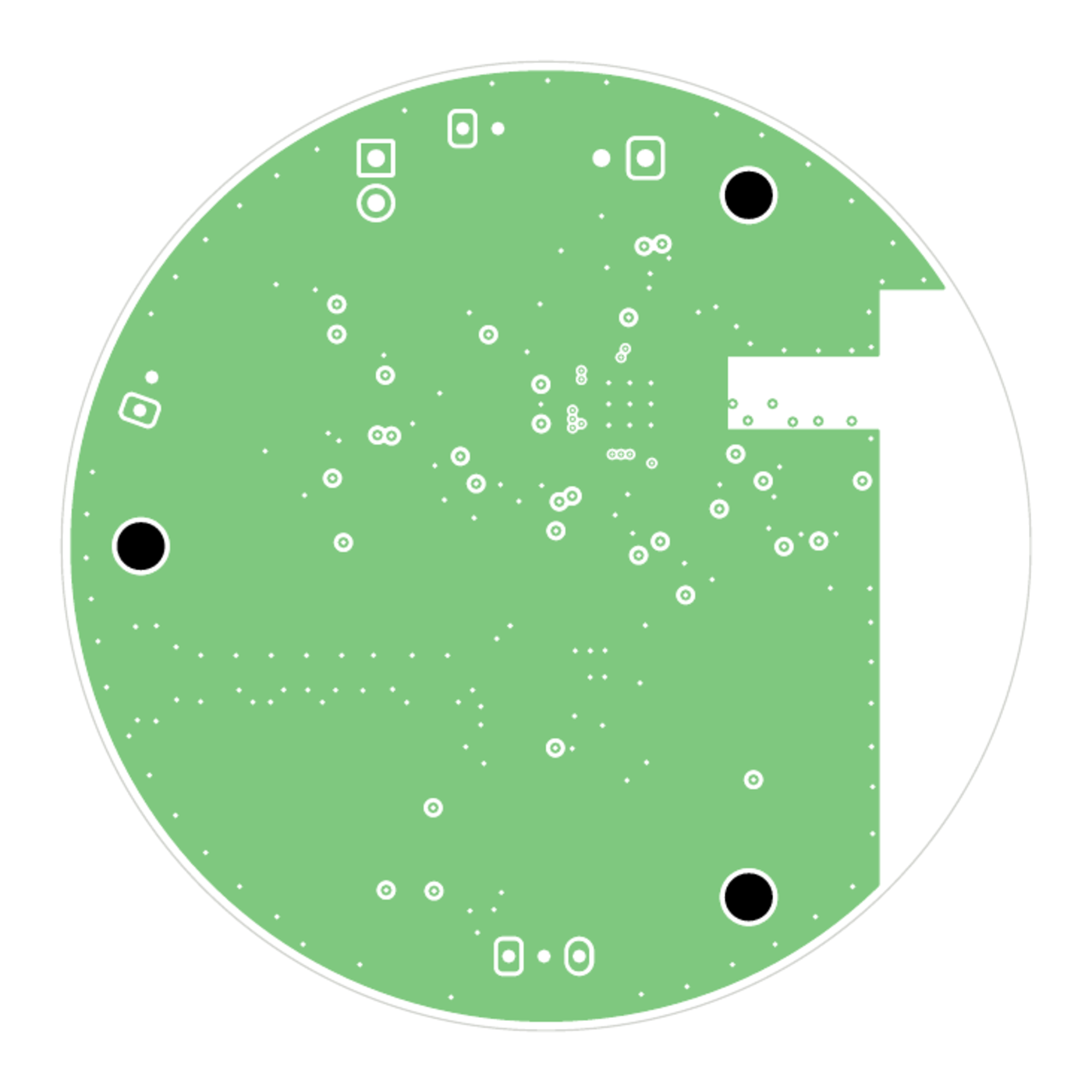 | 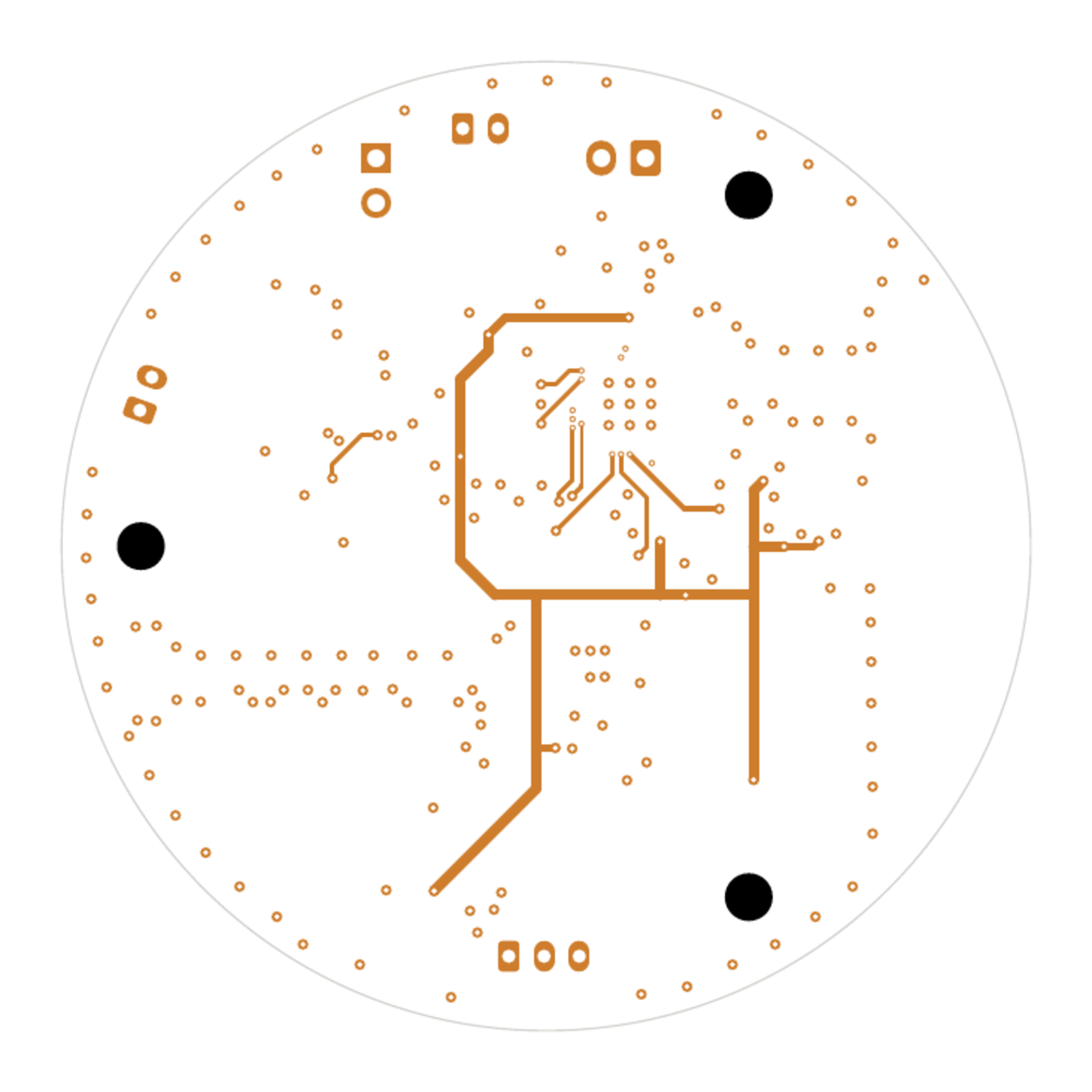 |
| Path | Contents |
|---|---|
hardware/rev-a/ | KiCad 10 project: five schematic sheets, PCB, symbol and footprint libraries, 3D models |
simulation/ | Coplanar-waveguide pre-check for the 868 MHz feed, and the plan for the 3D model |
docs/ | Assembly, fabrication and PCBA notes, stackup, impedance, schematic PDF |
firmware/ | Reserved for the node firmware |
Open the project with KiCad 10:
kicad hardware/rev-a/lora-node.kicad_proThe board is drawn for JLCPCB 4-layer fabrication and Standard PCBA, with X-ray
inspection for the aQFN73 and BME280. Paste, stencil and panel choices are in
docs/fab-notes.md,
docs/assembly-notes.md and
docs/pcba-notes.md.
The fabrication package for a release — gerbers, drill file, job file, BOM and CPL — is attached to the release rather than committed here.
Rev A is frozen and has not been fabricated yet. The design is complete through DRC, ERC and schematic/board parity.
Released under the CERN Open Hardware Licence Version 2 – Permissive.
| Qty | Value | Footprint | References |
|---|---|---|---|
| 12 | 100nF | Capacitor_SMD:C_0402_1005Metric | C12, C13, C14, C15, C25, C26, C29, C30, C31, C32, C33, C35 |
| 4 | 10uF | Capacitor_SMD:C_0805_2012Metric | C6, C7, C8, C28 |
| 4 | 12pF | Capacitor_SMD:C_0402_1005Metric | C19, C20, C21, C22 |
| 4 | 4.7uF | Capacitor_SMD:C_0603_1608Metric | C10, C11, C34, C36 |
| 4 | 6.8M | Resistor_SMD:R_0402_1005Metric | R3, R4, R8, R10 |
| 3 | 10k | Resistor_SMD:R_0402_1005Metric | R9, R17, R18 |
| 3 | 10nF | Capacitor_SMD:C_0402_1005Metric | C2, C4, C23 |
| 3 | 1uF | Capacitor_SMD:C_0603_1608Metric | C16, C17, C27 |
| 3 | 47pF | Capacitor_SMD:C_0402_1005Metric | C39, C40, C44 |
| 3 | AO3401A | Package_TO_SOT_SMD:SOT-23 | Q1, Q2, Q3 |
| 3 | Fiducial | Fiducial_1mm_Mask2mm | FID1, FID2, FID3 |
| 3 | M2.5 | MountingHole_2.7mm_M2.5_DIN965 | H1, H2, H3 |
| 2 | 0.2pF | Capacitor_SMD:C_0402_1005Metric | C41, C50 |
| 2 | 100k | Resistor_SMD:R_0402_1005Metric | R13, R16 |
| 2 | 1k | Resistor_SMD:R_0402_1005Metric | R15, R19 |
| 2 | 2.7nH | Inductor_SMD:L_0402_1005Metric | L14, L15 |
| 2 | 32MHz | Crystal:Crystal_SMD_2016-4Pin_2.0x1.6mm | X1, X3 |
| 2 | 5.6pF | Capacitor_SMD:C_0402_1005Metric | C43, C45 |
| 1 | +3V3 | TestPoint:TestPoint_Pad_D1.0mm | TP2 |
| 1 | +BATT | TestPoint:TestPoint_Pad_D1.0mm | TP1 |
| 1 | 0.5A | Fuse:Fuse_1812_4532Metric | F1 |
| 1 | 0.5pF | Capacitor_SMD:C_0402_1005Metric | C52 |
| 1 | 0.8pF | Capacitor_SMD:C_0402_1005Metric | C51 |
| 1 | 0R | Resistor_SMD:R_0402_1005Metric | R20 |
| 1 | 1.2pF | Capacitor_SMD:C_0402_1005Metric | C53 |
| 1 | 1.8pF | Capacitor_SMD:C_0402_1005Metric | C49 |
| 1 | 10nH | Inductor_SMD:L_0402_1005Metric | L17 |
| 1 | 10uF/10V | Capacitor_SMD:C_0805_2012Metric | C1 |
| 1 | 10uH | Inductor_SMD:L_0603_1608Metric | L10 |
| 1 | 15nH | Inductor_SMD:L_0402_1005Metric | L11 |
| 1 | 15uH | Inductor_SMD:L_0603_1608Metric | L12 |
| 1 | 1M | Resistor_SMD:R_0402_1005Metric | R7 |
| 1 | 2.2uH | Inductor_SMD:L_1210_3225Metric | L3 |
| 1 | 22nH | Inductor_SMD:L_0402_1005Metric | L18 |
| 1 | 22uH | Inductor_SMD:L_1210_3225Metric | L1 |
| 1 | 2x3 1.27 | Connector_PinHeader_1.27mm:PinHeader_2x03_P1.27mm_Vertical_SMD | J3 |
| 1 | 3.0M | Resistor_SMD:R_0402_1005Metric | R11 |
| 1 | 3.0pF | Capacitor_SMD:C_0402_1005Metric | C42 |
| 1 | 3.3pF | Capacitor_SMD:C_0402_1005Metric | C46 |
| 1 | 3.9pF | Capacitor_SMD:C_0402_1005Metric | C48 |
| 1 | 32.768kHz | Crystal:Crystal_SMD_3215-2Pin_3.2x1.5mm | X2 |
| 1 | 4.0pF | Capacitor_SMD:C_0402_1005Metric | C47 |
| 1 | 4.7M | Resistor_SMD:R_0402_1005Metric | R14 |
| 1 | 4.7nH | Inductor_SMD:L_0402_1005Metric | L19 |
| 1 | 470nF | Capacitor_SMD:C_0402_1005Metric | C24 |
| 1 | 47nF | Capacitor_SMD:C_0402_1005Metric | C18 |
| 1 | 47nH | Inductor_SMD:L_0402_1005Metric | L13 |
| 1 | 8.2nH | Inductor_SMD:L_0402_1005Metric | L16 |
| 1 | BME280 | Package_LGA:Bosch_LGA-8_2.5x2.5mm_P0.65mm_ClockwisePinNumbering | U5 |
| 1 | BQ25570 | Package_DFN_QFN:QFN-20-1EP_3.5x3.5mm_P0.5mm_EP2x2mm | U1 |
| 1 | EXT_NTC | Connector_JST:JST_XH_B2B-XH-A_1x02_P2.50mm_Vertical | TH1 |
| 1 | LiFePO4 | Connector_JST:JST_PH_B2B-PH-K_1x02_P2.00mm_Vertical | J2 |
| 1 | MEAS | Connector_PinHeader_2.54mm:PinHeader_1x02_P2.54mm_Vertical | JP1 |
| 1 | MM8130-2600 | lora-node:COAXIAL-SWF | J6 |
| 1 | NTC | TestPoint:TestPoint_Pad_D1.0mm | TP6 |
| 1 | SCL | TestPoint:TestPoint_Pad_D1.0mm | TP8 |
| 1 | SDA | TestPoint:TestPoint_Pad_D1.0mm | TP7 |
| 1 | SOIL | Connector_JST:JST_PH_B3B-PH-K_1x03_P2.00mm_Vertical | J4 |
| 1 | SOLAR | Connector_JST:JST_PH_B2B-PH-K_1x02_P2.00mm_Vertical | J1 |
| 1 | SRV05-4 | Package_TO_SOT_SMD:SOT-23-6 | D2 |
| 1 | SX1262 | Package_DFN_QFN:QFN-24-1EP_4x4mm_P0.5mm_EP2.6x2.6mm | U4 |
| 1 | TPS61099 | Package_SON:WSON-6-1EP_2x2mm_P0.65mm_EP1x1.6mm | U2 |
| 1 | U.FL | Connector_Coaxial:U.FL_Hirose_U.FL-R-SMT-1_Vertical | J5 |
| 1 | VIN | TestPoint:TestPoint_Pad_D1.0mm | TP4 |
| 1 | VSTOR | TestPoint:TestPoint_Pad_D1.0mm | TP5 |
| 1 | nRF52840 | Package_DFN_QFN:Nordic_AQFN-73-1EP_7x7mm_P0.5mm | U3 |
| 1 | ~ | TestPoint:TestPoint_Pad_D1.0mm | TP3 |
110 parts, built around the SX1262IMLTRT, NRF52840-QIAA-R, BME280 and TPS61099DRV. The full list of its parts is on this page, with links to each part's symbol and footprint where PCBKit's library has them.
From the Mehdi-Ldj/lora-ble-sensor-node repository on GitHub, at the commit this page was made from: the board is hardware/rev-a/lora-node.kicad_pcb and its schematic hardware/rev-a/lora-node.kicad_sch. PCBKit opens the board in the browser, with nothing to install.
Its repository publishes it under the CERN-OHL-P-2.0 licence: you may reuse it on that licence's terms (keep the author's notice, and for a copyleft licence share your changes alike).
EnAccess/Cicada-WiSUN-HW
IoT Communications Module for Energy Access. A quick way to get production ready, bi-directional communications for your IoT embedded device.

tmpk13/cc1200-balloon
High altitude balloon payload: a CC1200 sub-GHz telemetry downlink and an air quality sensor stack, hosted by a Seeed Wio-E5 module. Four-layer 50 x 30 mm board, routed.


ngrabbs/ember
Open pvpanel.kicadpro with KiCad 10. The project contains the recovered schematic, routed PCB, project-local footprint libraries, and solar-module STEP model.


Gamecard/k2-plus-cm5
K2 Plus CM5 – Creality K2 Plus mit Upstream-Klipper auf einem Raspberry Pi CM5