10 layers224.5 × 160 mm
Haasoscope pro adc fpga board
drandyhaas/HaasoscopePro
Affordable 2 GHz 3.2 GS/s 12 bit open-source open-hardware expandable USB real-time oscilloscope
586 parts485MIT

 karimf1/buck-converter
This project showcases a synchronous buck converter module, demonstrating advanced power PCB layout skills. It features techniques like minimized switching loop areas, strategic ground planes, isolated feedback traces. The README includes an efficiency curve mapping performance across various loads.
Sync buck is an open-source printed circuit board by karimf1, from the karimf1/buck-converter repository on GitHub, published under the MIT licence. It is a 4-layer board of 100 × 70 mm with 58 parts on 17 nets, routed with 146 tracks and 79 vias.
It is built around the LMR33630ADDA and SMBJ24A. Its parts include 18 capacitors, 8 resistors, 4 diodes, 4 connectors and 2 ICs. It belongs with the power boards of this library.


The same synchronous buck converter laid out twice on one board — once properly, once with the switching loop stretched, the feedback trace run beside the switch node, and the thermal vias cut from six to two — so the cost of bad power layout can be measured instead of asserted.
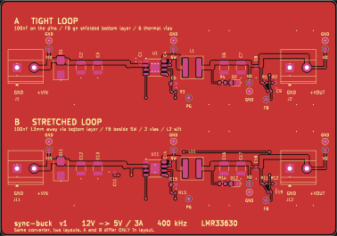
Three claims about power layout, in order of how much they matter:
Cin → high-side FET → low-side FET → Cin carries di/dt, and only its
enclosed area sets the switch-node ringing. Most people who "know" to
minimise loop area cannot say which loop.Channel B breaks all three on purpose. Everything else about the two channels is identical.
Measured out of the board file:
| channel A | channel B | |
|---|---|---|
| input cap → VIN pin, total reach | 3.51 mm | 19.41 mm |
| enclosed hot-loop area | 2.23 mm² | 12.33 mm² |
| vias in the hot loop | 0 | 2 |
| thermal vias under the exposed pad | 6 | 2 |
| FB on the top layer within 10 mm of SW / L | 1.2 mm | 26.7 mm |
| FB on shielded (inner-referenced) layers | 30.4 mm | 18.9 mm |
| closest FB-to-SW approach, same layer | 3.76 mm | 2.27 mm |
| L2 ground plane under the hot loop | continuous | 10 × 12 mm slit |
| schematic, parts, values, footprints | identical | identical |
 |  |
| A — the 100 nF sits across pins 1 and 2, no vias in the loop. | B — the same part, 9 mm away, reached through two vias. |
| parameter | value | why |
|---|---|---|
| Vin | 7 – 18 V (12 V nominal) | wide enough that the duty cycle visibly moves in the data |
| Vout | 5.02 V, resistor-set | 40.2 k / 10.0 k from a 1.0 V reference |
| Iout | 3 A | 15 W — a real thermal problem, still safe on a bench |
| fsw | 400 kHz | fixed on the LMR33630A |
| Inductor ripple | 24 % at 12 V, 30 % worst case at 18 V | 10 µH, Bourns SRP6060FA-100M |
| Output ripple | 6.9 mV pk-pk predicted at 3 A | 2 × 22 µF, derated to 33 µF at bias |
| Board | 100 × 70 mm, 4-layer, 1.6 mm, ENIG | L2 is a solid ground plane |
400 kHz was chosen for measurability, not optimality. It keeps the fundamental three decades below the parasitic ring so the two are separable on a lab scope, and it keeps the inductor big enough to hand-place. A product would switch faster and say so.
An internally compensated controller was chosen deliberately. Giving up the control loop is what lets the project be about layout and measurement instead of about compensation networks. It is a scoping decision, and it costs the project any claim about crossover frequency or phase margin.
Nothing is copied from the typical-application circuit. design/spec.py is the
single source of truth — the derivation and the schematic generator both import
it, so a value cannot be changed in one place and stale in the other.
Two details worth pulling out, because they separate people who have built things from people who have read about them:
Iout·√(D(1−D)) peaks at 1.5 A inside
this input range. That is real current into a ceramic, and it is why there
are two 1210s rather than one.The instrumentation choices matter as much as the circuit, because a bad measurement of a good board is indistinguishable from a bad board:
√(Σ(δx/x)²) ≈ ±1 %. "92 % ± 1 %", never "92.34 %" — quoting four
significant figures from a handheld meter is the fastest way to say you have
not thought about measurement.The result the board exists for is measurement 4: switch-node ringing, A against B, same scope, same probe, same geometry.
| Qty | Value | Footprint | References |
|---|---|---|---|
| 4 | 10uF/50V | Capacitor_SMD:C_1210_3225Metric | C2, C3, C12, C13 |
| 4 | 22uF/25V | Capacitor_SMD:C_1210_3225Metric | C6, C7, C16, C17 |
| 2 | 10.0k 1% | Resistor_SMD:R_0402_1005Metric | R2, R12 |
| 2 | 100k | Resistor_SMD:R_0402_1005Metric | R3, R13 |
| 2 | 100nF/16V | Capacitor_SMD:C_0402_1005Metric | C4, C14 |
| 2 | 100nF/25V | Capacitor_SMD:C_0402_1005Metric | C8, C18 |
| 2 | 100nF/50V | Capacitor_SMD:C_0402_1005Metric | C1, C11 |
| 2 | 10uH | Inductor_SMD:L_Bourns_SRP6060FA | L1, L11 |
| 2 | 1uF/16V | Capacitor_SMD:C_0603_1608Metric | C5, C15 |
| 2 | 2.2k | Resistor_SMD:R_0603_1608Metric | R4, R14 |
| 2 | 22pF C0G | Capacitor_SMD:C_0402_1005Metric | C9, C19 |
| 2 | 40.2k 1% | Resistor_SMD:R_0402_1005Metric | R1, R11 |
| 2 | FB | TestPoint:TestPoint_Pad_D1.5mm | TP5, TP15 |
| 2 | INPUT | TerminalBlock_Phoenix:TerminalBlock_Phoenix_MKDS-1,5-2-5.08_1x02_P5.08mm_Horizontal | J1, J11 |
| 2 | LMR33630ADDA | Package_SO:Texas_HSOP-8-1EP_3.9x4.9mm_P1.27mm | U1, U11 |
| 2 | OUTPUT | TerminalBlock_Phoenix:TerminalBlock_Phoenix_MKDS-1,5-2-5.08_1x02_P5.08mm_Horizontal | J2, J12 |
| 2 | PG | TestPoint:TestPoint_Pad_D1.5mm | TP6, TP16 |
| 2 | SMBJ24A | Diode_SMD:D_SMB | D1, D11 |
| 2 | SW | TestPoint:TestPoint_Pad_D1.5mm | TP1, TP11 |
| 2 | SWG | TestPoint:TestPoint_Pad_D1.5mm | TP2, TP12 |
| 2 | VING | TestPoint:TestPoint_Pad_D1.5mm | TP8, TP18 |
| 2 | VINS | TestPoint:TestPoint_Pad_D1.5mm | TP7, TP17 |
| 2 | VOG | TestPoint:TestPoint_Pad_D1.5mm | TP10, TP20 |
| 2 | VOS | TestPoint:TestPoint_Pad_D1.5mm | TP9, TP19 |
| 2 | VRIP | TestPoint:TestPoint_Pad_D1.5mm | TP3, TP13 |
| 2 | VRIPG | TestPoint:TestPoint_Pad_D1.5mm | TP4, TP14 |
| 2 | green | LED_SMD:LED_0805_2012Metric | D2, D12 |
drandyhaas/HaasoscopePro
Affordable 2 GHz 3.2 GS/s 12 bit open-source open-hardware expandable USB real-time oscilloscope

jamarju/c64-psu
Efficient Commodore 64 power supply with overvoltage + overcurrent protection

Andre1Becker/GalvOS
Open-source ESP32-S3 laser show controller — built to replace proprietary OEM controllers in RGB galvo laser projectors

Coen-Lab/exp-control-board
Hardware and firmware for an experimental control board for scientific rigs

ErdemA33/stm32f405-flight-controller
Open-source ArduPilot-compatible flight controller for fixed-wing UAVs. STM32F405, 4-layer KiCad design, built in 5 modular stages.

lhr-solar/PS-MotorControllerInterfacePCB
Provides power conversion/protection and fan control for the Prohelion WaveSculptor 22 motor controller

kfilipekk/iridium_drone
STM32H743 flight controller that navigates without GPS from Iridium satellite Doppler

KareemOye/USB_POWER_SUPPLY_PCB
12 V to 5 V USB step-down supply based on the LM2596-ADJ, designed in KiCad
It measures 100 × 70 mm and has 4 copper layers, 1.6 mm thick.
58 parts, built around the LMR33630ADDA and SMBJ24A. The full list of its parts is on this page, with links to each part's symbol and footprint where PCBKit's library has them.
From the karimf1/buck-converter repository on GitHub, at the commit this page was made from: the board is sync-buck.kicad_pcb and its schematic sync-buck.kicad_sch. PCBKit opens the board in the browser, with nothing to install.
Its repository publishes it under the MIT licence: you may reuse it on that licence's terms (keep the author's notice, and for a copyleft licence share your changes alike).