
2 layers145.1 × 38 mm
USB POWER SUPPLY
KareemOye/USB_POWER_SUPPLY_PCB
12 V to 5 V USB step-down supply based on the LM2596-ADJ, designed in KiCad
13 parts1

 KareemOye/USB_POWER_SUPPLY_PCB1
12 V to 5 V USB step-down supply based on the LM2596-ADJ, designed in KiCad
4 LAYER POWER SUPPLY copy is an open-source printed circuit board by KareemOye, from the KareemOye/USB_POWER_SUPPLY_PCB repository on GitHub. It is a 4-layer board of 40.5 × 37 mm with 30 parts on 11 nets, routed with 112 tracks and 23 vias.
It is built around the LMR33630ADDA. Its parts include 12 capacitors, 4 resistors, 2 connectors, 1 IC and 1 diode. It belongs with the power boards of this library.
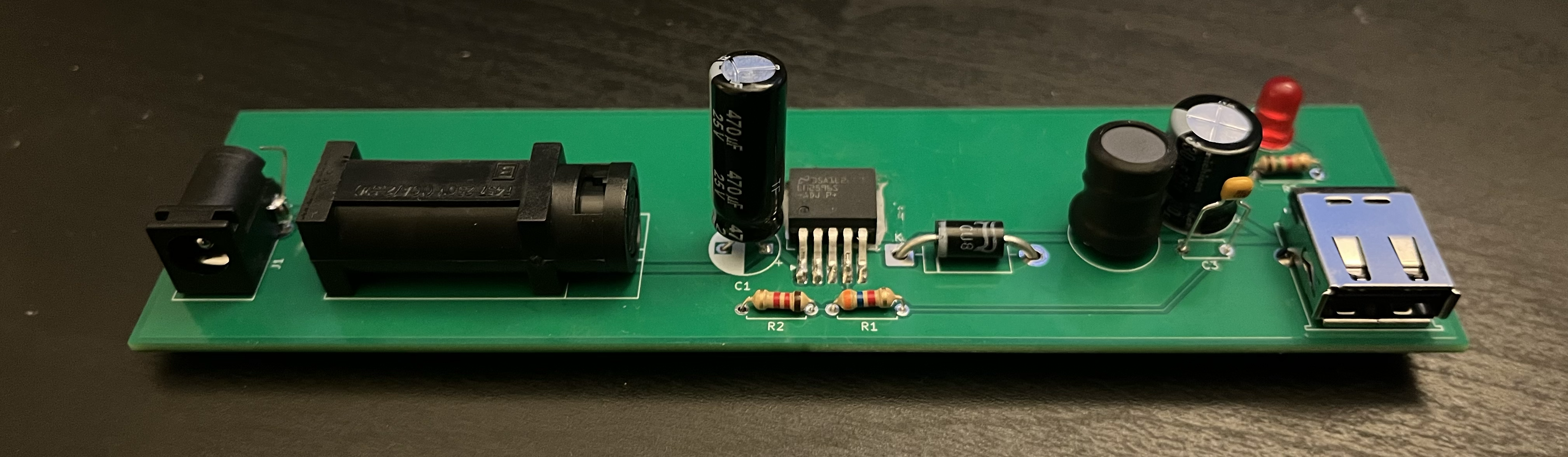
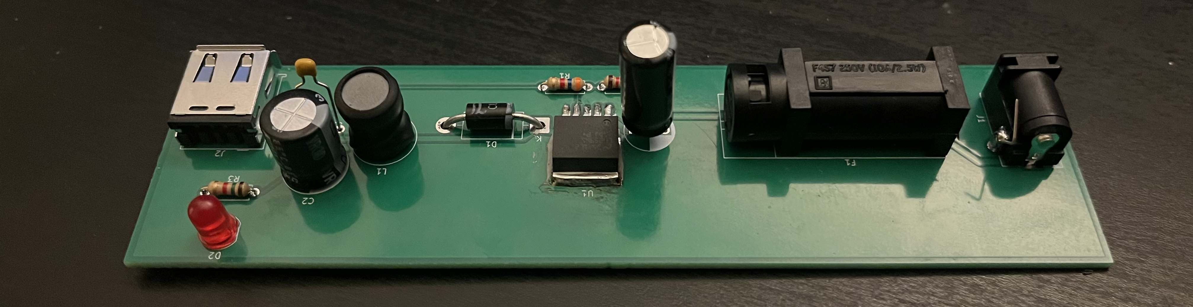
I started this project shortly before beginning my electrical engineering studies, as a way to learn electronics and circuit design through hands-on experience. A 12 V to 5 V USB step-down supply seemed like a good first PCB build, and having now designed and assembled it, I think that was the right call.
I went with a buck converter rather than a linear regulator, since dropping 12 V to 5 V linearly would waste a very significant amount of power as heat. The LM2596S-ADJ handles the switching, and a 1N5822 Schottky diode carries the inductor current while the internal switch is off. The feedback pin regulates to 1.23 V, so the 3.6 kΩ and 1.2 kΩ divider sets the output to about 4.9 V, and a 47 µH inductor smooths the current.
On the input side, a 1.6 A slow-blow fuse protects against shorts and a 470 µF capacitor supplies the pulsed current the converter draws when switching. At the output, a 330 µF electrolytic and a 100 nF ceramic reduce ripple, the USB D+ and D- lines are shorted so devices recognise it as a charger, and a power LED shows when the output is live.
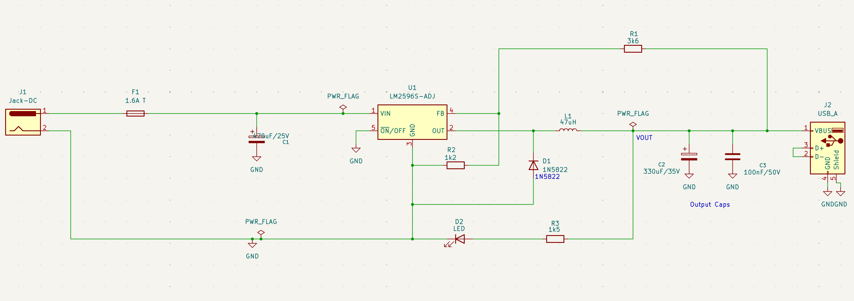
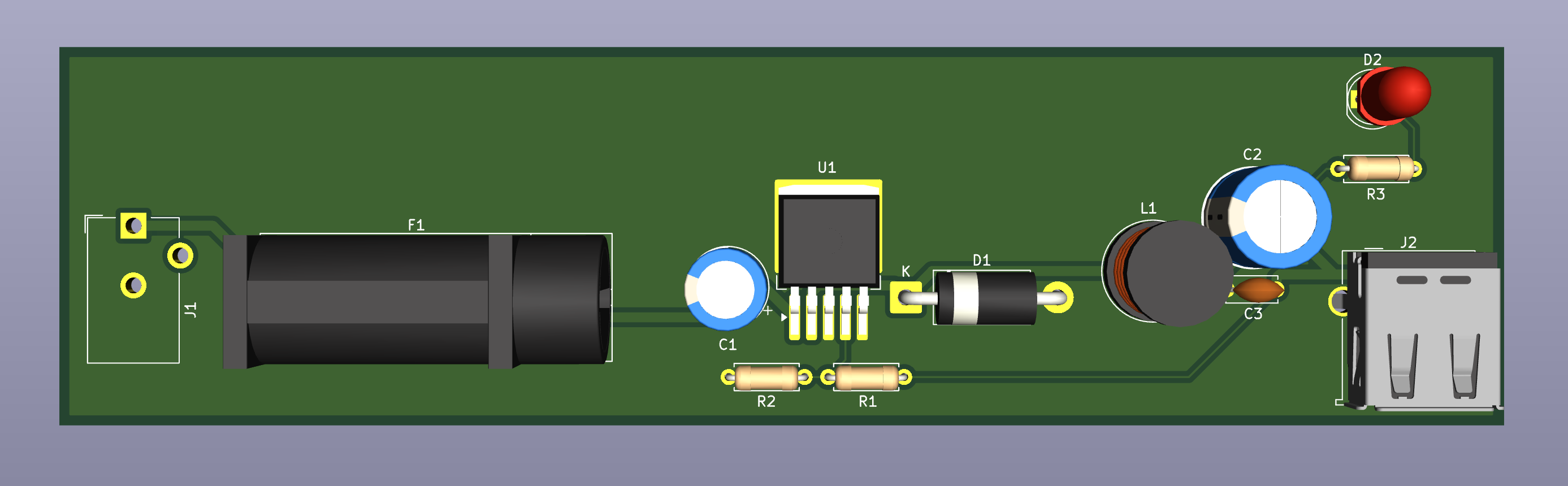
The board is a 2-layer approximately 145 × 38 mm design routed in KiCad, with one SMD component and the rest being through-hole and a ground pour on the bottom layer. I kept the input capacitor, LM2596, diode and inductor close together to keep the high-current switching loop small, which reduces noise and ringing.
The feedback trace is routed away from the inductor and switching node so the output regulation isn't disturbed, and the power traces are widened to 1 mm to handle the current.
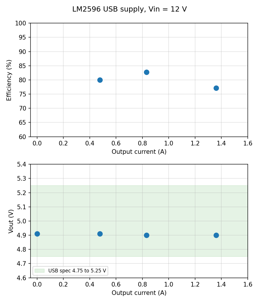
Measured at Vin = 12 V with resistive loads (10.3 Ω, 5.9 Ω, 3.6 Ω), Vout taken at the USB connector and input power from the bench supply readout.
Efficiency is about 80 to 83 % up to 0.8 A and drops to about 77 % at 1.36 A, where the board runs very hot (around 2 W of losses). Vout stays between 4.90 and 4.91 V from no load to 1.36 A, well inside the USB spec.
This was my first time taking a circuit all the way from schematic to a working board. I learned how a buck converter works in practice, how to read a datasheet to choose supporting components, and how much layout matters for switching circuits. The build also taught me the practical side: footprints, ordering parts and hand soldering.
Looking back, the layout is quite spread out and wasn't optimized for size or performance. The next revision applies what I learned here, with SMD components, a tighter layout and a 4-layer stackup, bringing the board down from 145 × 38 mm to 41 × 37 mm.
I am making a second board with the same function but a far more compact 4-layer design, 41 × 37 mm, built around the TI LMR33630. Unlike the LM2596, it's a synchronous converter with an integrated low-side switch, so the Schottky diode is gone and efficiency should improve, especially at higher loads. It also switches at 400 kHz instead of 150 kHz, which allows a smaller 10 µH inductor and ceramic output capacitors in place of the large electrolytic. The divider is now 100 kΩ / 24.9 kΩ against a 1.0 V reference, which would make the output 5.02 V according to calculation.
The board has already been designed and routed in KiCad, so the remaining steps are ordering parts, assembly and testing.
Once the second board is assembled and ready I'll compare the two boards on efficiency, output ripple and temperature.


| Qty | Value | Footprint | References |
|---|---|---|---|
| 6 | TestPoint | TestPoint:TestPoint_Pad_D1.5mm | TP1, TP2, TP3, TP4, TP5, TP6 |
| 4 | 22uF 25V | Capacitor_SMD:C_1210_3225Metric | C6, C7, C8, C9 |
| 2 | 100k | Resistor_SMD:R_0603_1608Metric | R1, R3 |
| 2 | 100nF | Capacitor_SMD:C_0603_1608Metric | C4, C10 |
| 2 | 10uF 50V | Capacitor_SMD:C_1210_3225Metric | C1, C12 |
| 1 | 1.6A T | Fuse:Fuse_1206_3216Metric | F1 |
| 1 | 10uH | Kareem_footprints:L_Eaton_EXL1V0606 | L1 |
| 1 | 1k5 | Resistor_SMD:R_0603_1608Metric | R4 |
| 1 | 1uF | Capacitor_SMD:C_0603_1608Metric | C5 |
| 1 | 220nF 50V | Capacitor_SMD:C_0603_1608Metric | C2 |
| 1 | 24.9k | Resistor_SMD:R_0603_1608Metric | R2 |
| 1 | 47uF 35V | Capacitor_SMD:CP_Elec_6.3x5.8 | C3 |
| 1 | DNP | Capacitor_SMD:C_0603_1608Metric | C11 |
| 1 | Jack-DC | Connector_BarrelJack:BarrelJack_CUI_PJ-102AH_Horizontal | J1 |
| 1 | LED | LED_SMD:LED_0805_2012Metric | D1 |
| 1 | LMR33630ADDA | Package_SO:Texas_HSOP-8-1EP_3.9x4.9mm_P1.27mm_ThermalVias | U1 |
| 1 | USB_A | Connector_USB:USB_A_Molex_67643_Horizontal | J2 |
The 28 most common of 30 parts.
KareemOye/USB_POWER_SUPPLY_PCB
12 V to 5 V USB step-down supply based on the LM2596-ADJ, designed in KiCad

drandyhaas/HaasoscopePro
Affordable 2 GHz 3.2 GS/s 12 bit open-source open-hardware expandable USB real-time oscilloscope

jamarju/c64-psu
Efficient Commodore 64 power supply with overvoltage + overcurrent protection

Andre1Becker/GalvOS
Open-source ESP32-S3 laser show controller — built to replace proprietary OEM controllers in RGB galvo laser projectors

Coen-Lab/exp-control-board
Hardware and firmware for an experimental control board for scientific rigs

ErdemA33/stm32f405-flight-controller
Open-source ArduPilot-compatible flight controller for fixed-wing UAVs. STM32F405, 4-layer KiCad design, built in 5 modular stages.

lhr-solar/PS-MotorControllerInterfacePCB
Provides power conversion/protection and fan control for the Prohelion WaveSculptor 22 motor controller

kfilipekk/iridium_drone
STM32H743 flight controller that navigates without GPS from Iridium satellite Doppler

lhr-solar/PS-PumpController
Controls speed of liquid cooling pump and fans for the main battery pack. Additionally, interprets data from temperature sensors and flowrate sensors for fan/pump control loop
It measures 40.5 × 37 mm and has 4 copper layers, 1.6 mm thick.
30 parts, built around the LMR33630ADDA. The full list of its parts is on this page, with links to each part's symbol and footprint where PCBKit's library has them.
From the KareemOye/USB_POWER_SUPPLY_PCB repository on GitHub, at the commit this page was made from: the board is v02 (in progress) /4_LAYER_POWER_SUPPLY copy.kicad_pcb and its schematic v01/USB_POWER_SUPPLY.kicad_sch. PCBKit opens the board in the browser, with nothing to install.
Its repository states no licence, so its author keeps all rights: ask KareemOye before reusing the design.