2 layers407 × 184 mm
TRS-80-Model I G E1
RetroStack/TRS-80-Model-I-G-E1
Hardware Replica of the TRS-80 Model I Revision G
230 parts57MIT

 hkzlab/ISA_EGA_CHIPS24
This board is and EGA clone based on a reversed PA-WTEGA card, based on the chipset by CHIPS (P82C435 + P82A436).
ISA EGA CHIPS is an open-source printed circuit board by hkzlab, from the hkzlab/ISA_EGA_CHIPS repository on GitHub. It is a 2-layer board of 131.1 × 108 mm with 68 parts on 160 nets, routed with 3,923 tracks and 269 vias.
It is built around the 27C256-17/J and 74LS153DC. Its parts include 29 capacitors, 15 ICs, 6 resistors, 6 connectors and 1 switch. It belongs with the retro computing and games boards of this library.

This board is and EGA clone based on a reversed PA-WTEGA card, based on the chipset by CHIPS (P82C435 + P82A436).
The chipset should be compatible with EGA, CGA, MDA and Hercules standards.
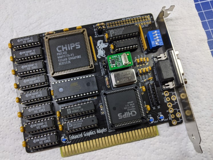
I take NO responsibility for what happens if you decide to build and use this card. Your computer might crash, catch fire or be destroyed in other nasty ways. You're encourauged to take what you deem fit from this, and use it in your projects!
The card as a bank of 5 dipswitches. Dipswitch 1-4 select the card video output mode, dipswitch 5 selects the IO address.
0 means switch open, 1 means closed.
NOTE: The meaning of each combination is dependant on the bios of the card. This list was taken from the TEVA-2 card's manual.
TODO: Test all the combinations provided in the TEVA-2 card manual
✅ means I tested the functionality and it works, ❌ means I tested the functionality and found issues, ? means that the functionality has yet to be tested.
| Component | Qty | Type / Value |
|---|---|---|
| TODO |
You can hardwire JP1 pins 1-2 and JP2 pins 2-3.
Connectors RCA 1 and RCA 2 are useless unless an expansion for the feature connector is used. You can leave them out.
This board was tested with Phoenix Video Bios V1.02 for P82C435.
Burn it on a 27C256 and plug it in U10.
These are issues found with this board, but that are also present in the original model I cloned.
The use of 35 frames, even in a 16-color game like Keen, demonstrates that ID was using VGA, not EGA, to develop the game ). It can be fixed in-game by enabling the "Fix Jerky Motion" option in the config screen.Thanks to Sergey Kiselev for his symbol/footprint library!
| Qty | Value | Footprint | References |
|---|---|---|---|
| 17 | 100nF | Capacitor_THT:C_Disc_D4.3mm_W1.9mm_P5.00mm | C1, C2, C3, C4, C5, C6, C7, C13, C18, C19, C20, C21, C22, C23, C24, C25 +1 |
| 8 | 22pF | Capacitor_THT:C_Disc_D4.3mm_W1.9mm_P5.00mm | C9, C10, C11, C12, C14, C15, C16, C17 |
| 8 | 41464 | Package_DIP:DIP-18_W7.62mm | U1, U3, U5, U7, U8, U9, U12, U14 |
| 3 | 10uF | Capacitor_THT:CP_Radial_D5.0mm_P2.50mm | C26, C28, C40 |
| 3 | 47 | Resistor_THT:R_Axial_DIN0207_L6.3mm_D2.5mm_P7.62mm_Horizontal | R3, R4, R6 |
| 3 | 74LS244 | Package_DIP:DIP-20_W7.62mm | U4, U13, U15 |
| 2 | 10k | Resistor_THT:R_Axial_DIN0207_L6.3mm_D2.5mm_P7.62mm_Horizontal | R1, R2 |
| 2 | 33 | Resistor_THT:R_Array_SIP8 | SIP3, SIP4 |
| 1 | 10k | Resistor_THT:R_Array_SIP9 | SIP2 |
| 1 | 16.257MHz | Custom_Oscillators:Oscillator_DIP-14-8 | OSC1 |
| 1 | 2.2k | Resistor_THT:R_Axial_DIN0207_L6.3mm_D2.5mm_P7.62mm_Horizontal | R5 |
| 1 | 25MHz | Custom_Oscillators:Oscillator_DIP-14-8 | OSC2 |
| 1 | 27C256 | Package_DIP:DIP-28_W15.24mm | U10 |
| 1 | 4.7k | Resistor_THT:R_Array_SIP9 | SIP1 |
| 1 | 47pF | Capacitor_THT:C_Disc_D4.3mm_W1.9mm_P5.00mm | C90 |
| 1 | 74LS153 | Package_DIP:DIP-16_W7.62mm | U6 |
| 1 | 82A436 | Package_LCC:PLCC-68_THT-Socket | U11 |
| 1 | 82C435 | Package_LCC:PLCC-84_THT-Socket | U2 |
| 1 | Bus_ISA_8bit | My_Components:Conn_Edge_PCB_ISA8 | J7 |
| 1 | Configuration | Package_DIP:DIP-10_W7.62mm_Socket | SW1 |
| 1 | Conn_01x03 | Connector_PinHeader_2.54mm:PinHeader_1x03_P2.54mm_Vertical | JP2 |
| 1 | Digital Output | Connector_Dsub:DSUB-9_Female_Horizontal_P2.77x2.84mm_EdgePinOffset7.70mm_Housed_MountingHolesOffset9.12mm | J6 |
| 1 | EGA Feature Connector | Connector_PinHeader_2.54mm:PinHeader_2x16_P2.54mm_Vertical | J1 |
| 1 | Feature Selector | Connector_PinHeader_2.54mm:PinHeader_1x04_P2.54mm_Vertical | JP3 |
| 1 | IRQ Enable | Connector_PinHeader_2.54mm:PinHeader_1x02_P2.54mm_Vertical | JP10 |
| 1 | Light Pen | Connector_PinHeader_2.54mm:PinHeader_1x06_P2.54mm_Vertical | J2 |
| 1 | Monitor Type | Connector_PinHeader_2.54mm:PinHeader_1x03_P2.54mm_Vertical | JP4 |
| 1 | RCA 1 | My_Components:Conn_RCA_Right | J3 |
| 1 | RCA 2 | My_Components:Conn_RCA_Right | J4 |
| 1 | ROM Type | Connector_PinHeader_2.54mm:PinHeader_1x03_P2.54mm_Vertical | JP1 |
RetroStack/TRS-80-Model-I-G-E1
Hardware Replica of the TRS-80 Model I Revision G

fortinsylvain/MyCpu
Home brew CPU Hardware with 1-bit ALU implementation using 74LSxx, a micro-code and assembler coded in C#.

reinauer/Amiga-Boot-Selector
This is a Floppy Switcher for the Amiga 500/2000. It allows you to switch DF0/DF1, making it possible to boot from either a Gotek drive or the internal floppy drive. without relying on AmigaOS.

clemarfolly/Microdigital-TK2000
Reprodução da PCB do TK-2000 da Microdigital, clone do Micro-Professor MPF-II


djtersteegc/Tandy-Color-Computer-Multi-Pak
Respin of the Tandy 26-3024 Multi-Pak (MPI) for the DIY builder.


It measures 131.1 × 108 mm and has 2 copper layers, 1.6 mm thick.
68 parts, built around the 27C256-17/J and 74LS153DC. The full list of its parts is on this page, with links to each part's symbol and footprint where PCBKit's library has them.
From the hkzlab/ISA_EGA_CHIPS repository on GitHub, at the commit this page was made from: the board is ISA_EGA_CHIPS.kicad_pcb and its schematic ISA_EGA_CHIPS.kicad_sch. PCBKit opens the board in the browser, with nothing to install.
Its repository states no licence, so its author keeps all rights: ask hkzlab before reusing the design.