
2 layers45 × 23 mm
Tiny
pengshulin/mcush
MCUSH application platform (personal toolkit: firmware platform, debugger, hardware, test and application framework)
53 parts103

 hkustenterprize/RM2025-Tiny-JLink16
Cheap, Smallest JLink-OB
RM2025-Tiny JLink is an open-source printed circuit board by hkustenterprize, from the hkustenterprize/RM2025-Tiny-JLink repository on GitHub, published under the AGPL-3.0 licence. It is a 2-layer board of 18.1 × 11.5 mm with 23 parts on 40 nets, routed with 205 tracks and 58 vias.
It is built around the STM32F103CBT6. Its parts include 11 capacitors, 4 resistors, 3 connectors, 2 ICs and 1 diode. It belongs with the STM32 boards of this library.
尺寸无敌, 地表最小 JLink-OB. 尺寸仅为 20x12x5mm.
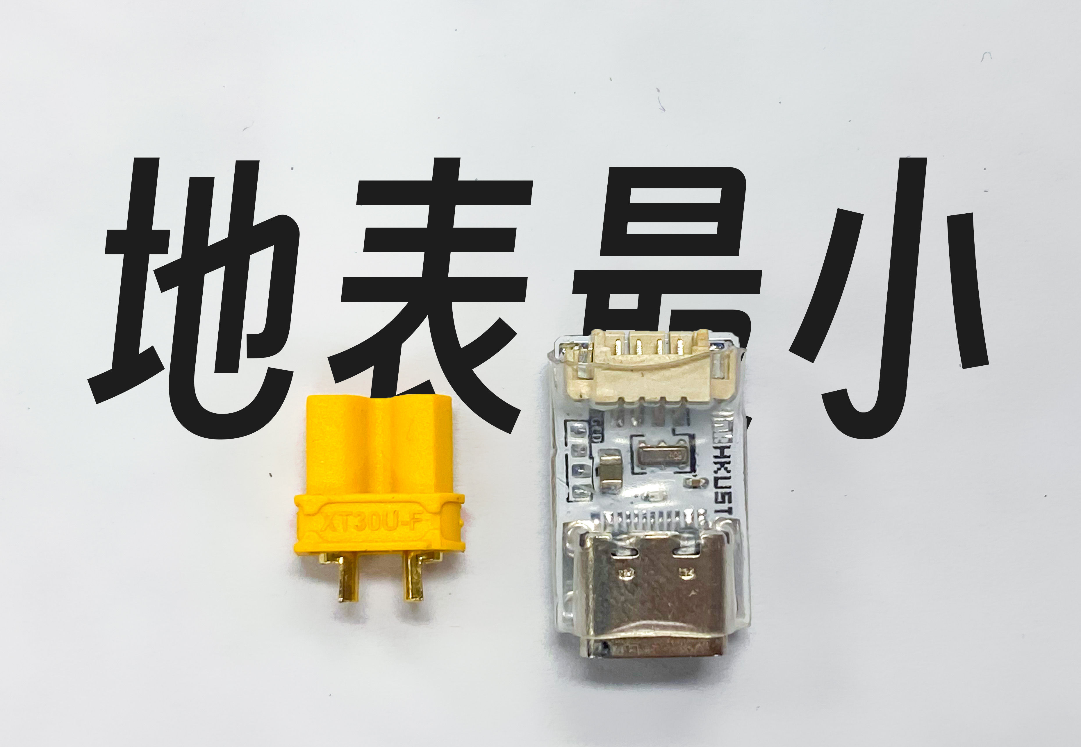
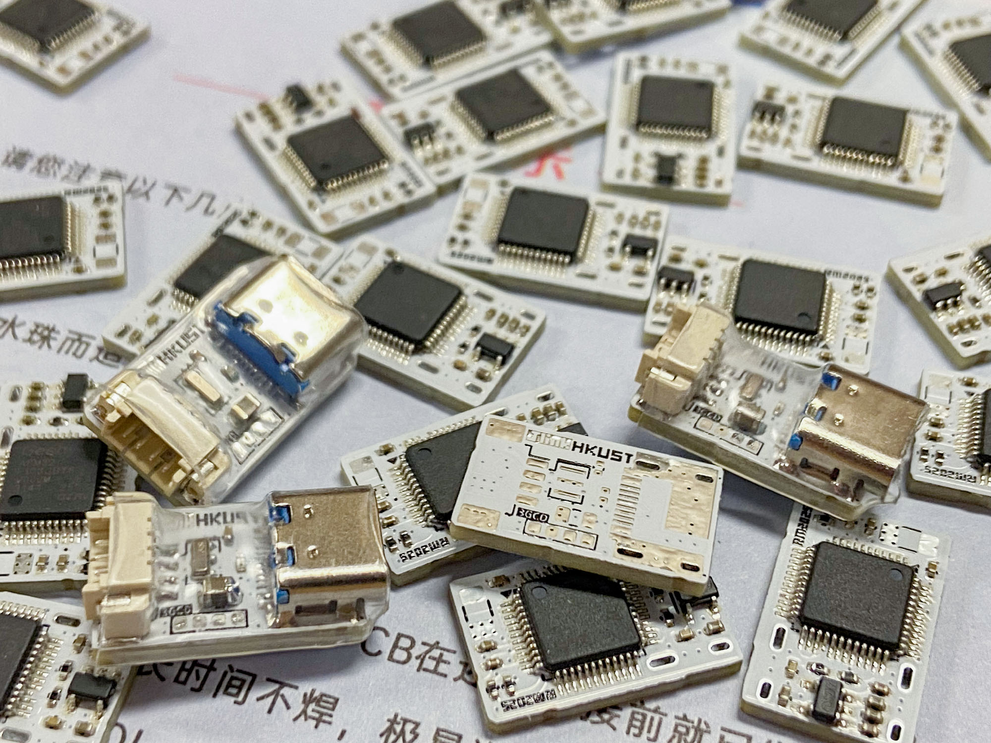
本赛季小批量做了一批, 使用体验不错, 非常优雅. 稳定性好, 固定在车上能较好地解决 JLink 断联的情况.
关键参数
| 参数 | 说明 |
|---|---|
| 尺寸 | 20x12x5mm (约为两个 XT30 头) |
| 支持固件 | JLink-OB, STLink V2, DAPLink |
| 接口 | Type-C, 四线 SWD, 兼容战队开源 G 板, 官方 C 板等 |
| 成本 | 批量 15 元 |
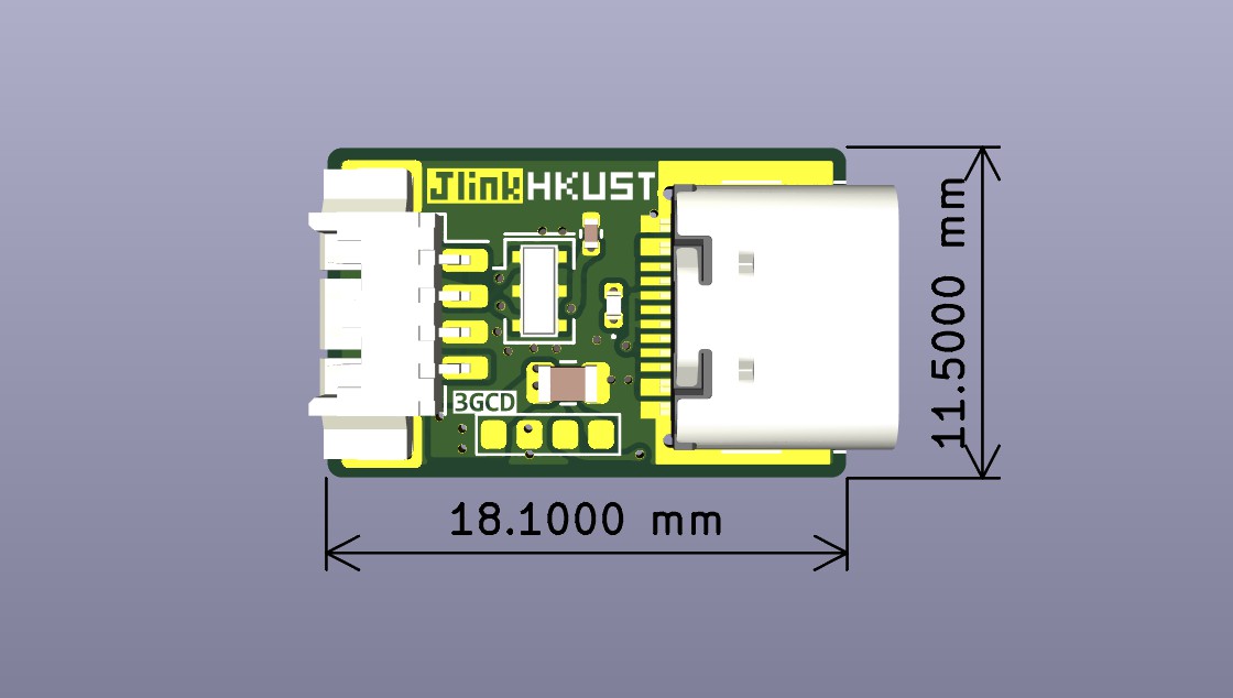
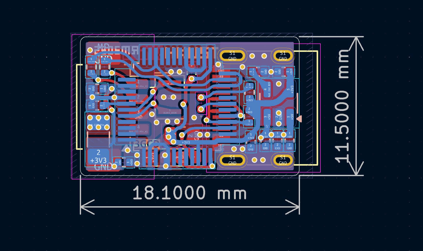
晶振采用村田 3215 晶振, 标称精度略低但小批量做的 50 个都能稳定进行 USB 通信. MCU 采用 APM32F103CBT6, 淘宝批量价格约 2.3 元/PCS. 可完美替代 STM32F103CBT6. 此外, 也可用 GD32F103CBT6 替代. LDO 采用对内常用 RS3236-3V3. 阻容使用 0402 封装.
焊接时需要将 Type-C 座子的塑料定位柱掰断, PCB 上删除了定位柱对应孔位. Type-C 座子底部焊盘请提前上锡, 增加机械强度.
与原版 JLink-OB 原理图相比, 调整了如下内容:
USB re-enum 相关电路参考: https://stm32world.com/wiki/STM32_USB_Device_Renumeration#google_vignette
此外, 为了进一步减小体积, 进行了一些激进的调整(不推荐):
实测, D+ 上拉电阻在 1K - 2K 内都可识别.
烧录口是正面 1.27mm-4P 焊盘, 引脚定义为: (从左到右) +3.3V, GND, SWCLK, SWDIO.
目前包含的固件有: STLink V2.1, JLink-OB
STLink 固件来自 https://github.com/lyplcr/JSTLINK_SW STLinkReflash.exe 来自 https://www.segger.com/downloads/jlink/. 需将几处条件跳转指令替换为 NOP 指令绕过芯片 UID 检查. STLinkReflash_190812_pached.exe 是笔者修改好的 STLinkReflash.exe, 可直接使用.
如果需要小批量烧录, 建议购买淘宝 1.27mm 单排4P 烧录夹具.
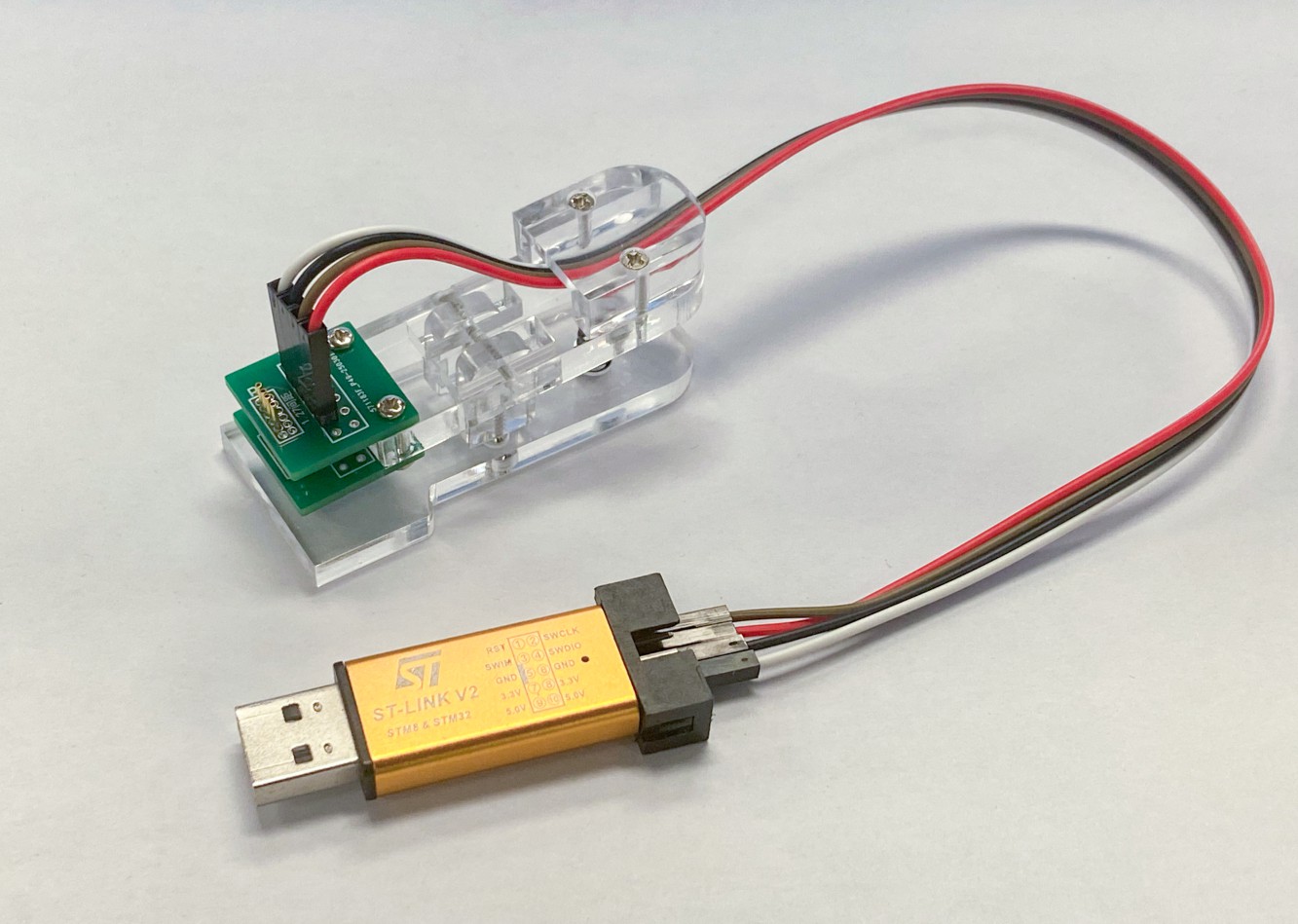
如果用 C-C 线连电脑需要将 CC 电阻加回来. 可以替换晶振与 LDO 选型, 进一步降低成本. 如果感兴趣的人多, 可以考虑 拼好板 均摊 SMT 价格. 批量做成本约 15 元/个.
WeChat: baoqi-zhong Email: zzhongas@connect.ust.hk
| Qty | Value | Footprint | References |
|---|---|---|---|
| 6 | 100nF | Capacitor_SMD:C_0402_1005Metric | C1, C2, C3, C9, C10, C12 |
| 3 | 4.7uF | Capacitor_SMD:C_0402_1005Metric | C6, C8, C11 |
| 2 | 1K | Resistor_SMD:R_0402_1005Metric | R1, R2 |
| 2 | 33R | Resistor_SMD:R_0402_1005Metric | R3, R4 |
| 1 | 10nF | Capacitor_SMD:C_0402_1005Metric | C7 |
| 1 | 10uF | Capacitor_SMD:C_0805_2012Metric | C5 |
| 1 | 1A | Fuse:Fuse_1206_3216Metric | F1 |
| 1 | 8MHz | Crystal:Resonator_SMD_Murata_CSTxExxV-3Pin_3.0x1.1mm | Y1 |
| 1 | JLINK_OUT | Connector_Molex:Molex_PicoBlade_53261-0471_1x04-1MP_P1.25mm_Horizontal | J2 |
| 1 | JLink_Upload | RM2024:1.25Upload | J1 |
| 1 | LED | LED_SMD:LED_0402_1005Metric | D1 |
| 1 | RS3236 | Package_TO_SOT_SMD:SOT-23-5 | U2 |
| 1 | STM32F103CBT6 | Package_QFP:LQFP-48_7x7mm_P0.5mm | U1 |
| 1 | USB_C_Receptacle_USB2.0 | RM2024:USB_C_Receptacle_HRO_TYPE-C-31-M-12_NO_HOLE | J3 |
pengshulin/mcush
MCUSH application platform (personal toolkit: firmware platform, debugger, hardware, test and application framework)

john0312/hitcon-pcb-badge
execute fw/merge.py to merge STM32CubeIDE generated main.c with user code in main.cc into main.cc.

laneboysrc/rc-headless-transmitter
DIY 2.4 GHz RC transmitter without display, configurable through smartphone or web browser


hkustenterprize/RM2025-Wireless-JLink
Wireless JLink-OB based on Allwinner V3S


electroniceel/stm32....c-breakout
A breakout module for STM32 microcontrollers in LQFP48 and UFQFPN48 footprint.

dilshan/usb-external-display
USB 10 digit seven segment display unit
It measures 18.1 × 11.5 mm and has 2 copper layers, 1.6 mm thick.
23 parts, built around the STM32F103CBT6. The full list of its parts is on this page, with links to each part's symbol and footprint where PCBKit's library has them.
From the hkustenterprize/RM2025-Tiny-JLink repository on GitHub, at the commit this page was made from: the board is Hardware/RM2025-Tiny-JLink.kicad_pcb and its schematic Hardware/RM2025-Tiny-JLink.kicad_sch. PCBKit opens the board in the browser, with nothing to install.
Its repository publishes it under the AGPL-3.0 licence: you may reuse it on that licence's terms (keep the author's notice, and for a copyleft licence share your changes alike).