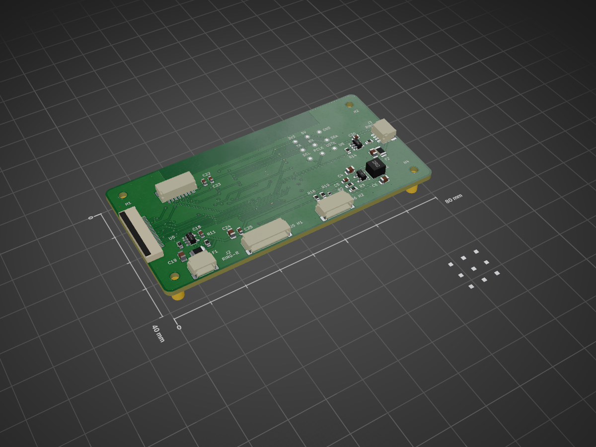
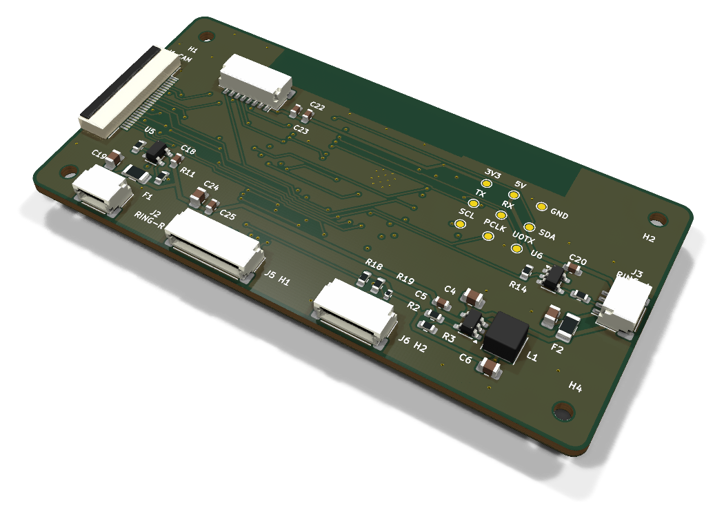
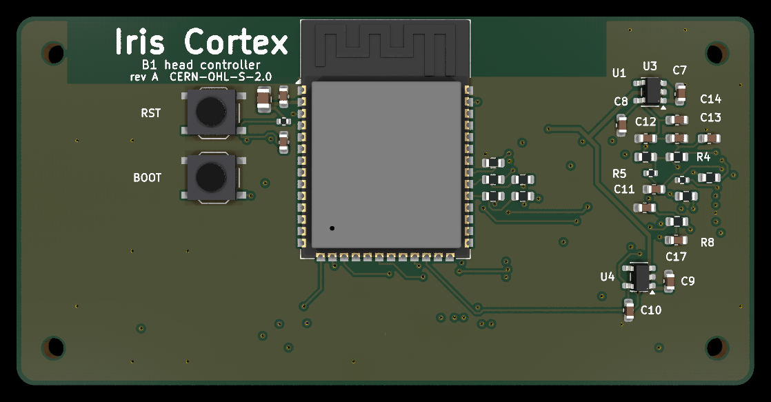
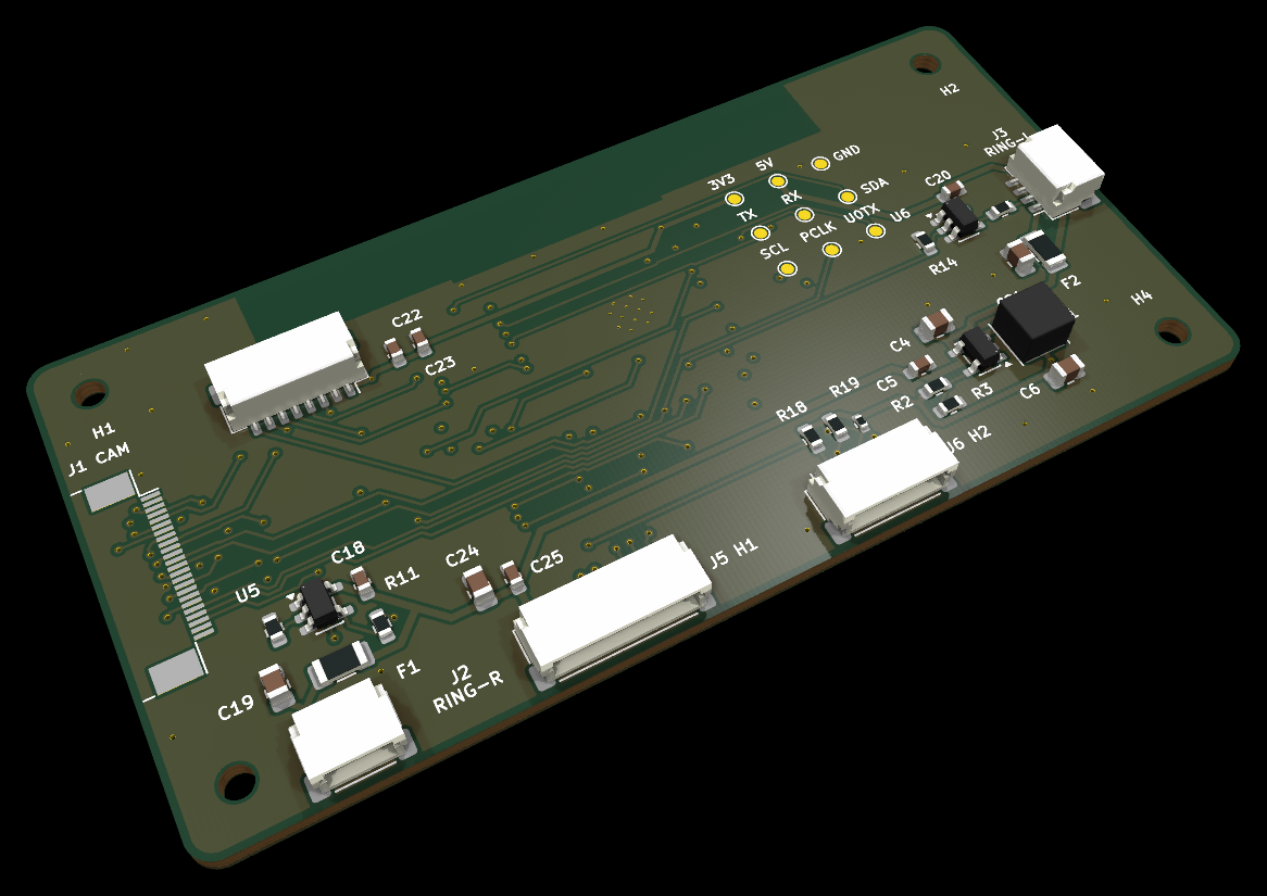
Iris cortex is an open-source printed circuit board by HeyPCB, from the HeyPCB/iris-cortex repository on GitHub, published under the CERN-OHL-S-2.0 licence. It is a 4-layer board of 80 × 40 mm with 77 parts on 63 nets, routed with 913 tracks and 117 vias.
It is built around the ESP32-S3-WROOM-1-N16R8, TLV62569DBVR-TP and SN74AHCT1G125DBVR(UMW), with the ME6211C12M5G-N, ME6211C28M5G-N and CC0603KRX7R9BB104 among its other parts. Its parts include 25 capacitors, 22 resistors, 6 ICs, 6 connectors and 2 switches. It belongs with the robots and motor control boards and the ESP32 boards of this library.
The head controller of Iris: an ESP32-S3 (16 MB flash, 8 MB PSRAM) with the eye camera's FPC, the iris-ring LED drivers and the harness to the brainstem and brow. It rides the tilt cradle.
Part of Iris, the human-eyed robot head, HeyPCB's open robot boards. Designed end to end with the HeyPCB method on
KiCad 10 (headless pipeline, Freerouting 2.4.1); every number below is measured on the files in this repository.
Mentions of ./run.sh, docs/rules/, blocks/ or parts/ refer to the heypcb-kicad SDK that produced them.
Iris Cortex is the head controller of Iris, an open-hardware robot head with human-like eyes. It
is board B1 of the Iris design spec (v0.1, 2026-10-03, section 4.1; not published, its binding
contracts are in the Iris system docs).
An ESP32-S3-WROOM-1-N16R8 runs the OV2640 camera in the right eye through a 24-pin FPC connector. Two
buffered outputs drive the WS2812C iris LED rings. Five JST SH headers carry the spec's binding harness
contracts to the Brainstem (B2), the Brow strip (B4) and the two iris rings (B3). The design was
made with the HeyPCB method on KiCad 10 (10.0.6), using heypcb-kicad's headless pipeline and
Freerouting 2.4.1. The input is the brief in board.json.
This board has not been fabricated, assembled or powered, and its firmware has not been written.
Every number below comes from KiCad and the pipeline, measured on the design files (report.json of the
final run, 2026-10-03). Nothing here has been tested on hardware.
Where it sits in Iris
It rides the tilt cradle. B1 is screwed to four Ø5 bosses with M2 heat-set inserts on the
cradle's rear plate (spec part P5). It tilts with the eyes, so the camera FPC only has to flex for
pan (one out-of-plane bend). The B1-B2 harnesses take the ±30° tilt as a bend near the axis.
Frame. In the head frame H at tilt 0 (origin between the eye centres, +X forward out of the
face, +Y robot-left, +Z up), the F face is at X = -52.0 and faces the eyes. The B face is at
X = -53.6 and rests on the bosses. Board coordinates map as Y = x - 40 and Z = 20 - y.
Board coordinates are mm from the outline's top-left corner, with x to the right and y down, seen
from F.
Neighbours.
The OV2640 module sits in the right eye at Y -39. Its FPC exits temporally (toward -Y), bends
back along -X, then runs +Y along B1's F face into J1.
B2 (the Brainstem) sits below, at Z -60. H1 and H2 leave B1's bottom edge toward it.
B4 (the Brow) sits above, at Z +50. BROW leaves upward.
The two iris rings (B3) are inside the eyes, at Y ±39.
v1 scope. Iris v1 has a fixed head (no neck), one camera (mono vision) and a stylised hard-shell
face. B1 follows the spec's design for that scope.
Features
ESP32-S3-WROOM-1-N16R8 (U1, LCSC C2913202): 16 MB flash, 8 MB octal PSRAM, Wi-Fi and BLE. It
sits on the B face, centred, with its antenna end at the top edge. Native USB 2.0 FS runs over H1
from B2's USB-C data port; there is no USB-serial bridge.
Camera.
J1 is a Jushuo AFC07-S24FCA-00: 24 pins at 0.5 mm, bottom contact, slide lock.
The camera pins use the ESP32-S3-EYE map, so esp-who and esp32-camera board configs apply unchanged.
SCCB has 4.7 k pull-ups to DOVDD. RESETB has 10 k to DOVDD and 100 nF to GND. PWDN has a 10 k
pull-down and also goes to GPIO46.
PCLK, VSYNC and HREF pass through 0 ohm links. They can be swapped for 33-100 ohm.
AVDD, DOVDD and DVDD each have 4.7 uF + 100 nF at the connector.
Camera supplies. U3 (ME6211C28) makes 2.8 V for AVDD + DOVDD. U4 (ME6211C12) makes 1.2 V for the
OV2640 core. For an OV3660 or OV5640 module, fit ME6211C15 (C53100) in U4's place: same footprint,
same pins.
Iris ring drivers.
Two SN74AHCT1G125 buffers (U5, U6) turn the RMT outputs on GPIO47 / GPIO48 into 5 V WS2812 data.
Each buffer has a 33 ohm series resistor, and a 100 k pull-down that keeps its input low through
reset.
Each ring is fed from 5V_SYS through its own 0.5 A resettable fuse (F1, F2), with 10 uF behind it.
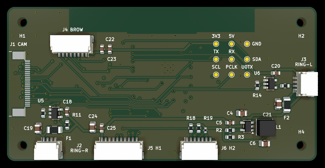
Harness headers (JST SH side entry, pinouts below): J5 H1 (SH-10), J6 H2 (SH-7), J4 BROW
(SH-8), J2 RING_R and J3 RING_L (SH-4). Every SH header on the board has a different pin count, except
the two interchangeable ring headers.
3V3 from a TLV62569 buck (U2): 2 A part, 2.2 uH, 3.327 V by its 100 k / 22 k divider.
System I2C bus master. The bus's only pull-ups (2.2 k) are on B1. nINT (the INA226 ALERT on B2)
has a 10 k pull-up here.
I2S, full duplex. BCLK and WS go to both B2 (amplifier) and B4 (microphones), each branch through
its own 33 ohm source resistor. The amplifier data goes out and the microphone data comes in
(100 k pull-down).
Bring-up.
BOOT (SW1) and RESET (SW2) buttons are on the B face.
Nine 1.0 mm test pads on the F face: 3V3, 5V, GND, TX, RX, SDA, SCL, PCLK and U0TX (the
ESP32-S3's ROM boot log).
Board.
80.0 x 40.0 mm with 2.0 mm fillets, 1.6 mm, 4 copper layers.
Layers: F.Cu signal / In1 GND plane / In2 signal with a 3V3 pour / B.Cu signal. F.Cu and B.Cu
have GND pours.
Measured on the final board file (kicad/iris_cortex.kicad_pcb).
Outline: 80.0 x 40.0 mm rectangle. Edge.Cuts fillets are r 2.0 mm, centred at (2, 2),
(78, 2), (2, 38) and (78, 38). The board is 1.6 mm thick (gerber job).
Holes: four Ø2.2 mm NPTH (MountingHole_2.2mm_M2) for M2 x 6 screws into the cradle's
heat-set inserts.
Hole
Board (x, y)
Head (X, Y, Z), F face
H1
(4.0, 4.0)
(-52.0, -36.0, +16.0)
H2
(76.0, 4.0)
(-52.0, +36.0, +16.0)
H3
(4.0, 36.0)
(-52.0, -36.0, -16.0)
H4
(76.0, 36.0)
(-52.0, +36.0, -16.0)
The bosses' faces are at X = -53.6 (the B face).
Connectors. All six connectors are on the F face, so their bodies stand from X = -52.0 toward the
eyes. The AFC07 is 2 mm tall (catalogue row C262567). For the SH housings, LCSC lists 2.9 mm and 4.32
mm body dimensions; the spec's F-face budget is 4.5 mm.
Ref
Harness
Body, board x range / y range
Body centre, head (Y, Z)
Opens toward
Mouth edge
Pin 1, board (x, y) / head (Y, Z)
J1
CAM FPC
x 0.00-4.50 / y 11.15-28.85
(-37.75, 0.00)
-x, the left edge (head -Y)
x 0.00 (Y -40.0)
(5.30, 14.25) / (-34.70, +5.75)
J2
RING_R
x 7.95-14.05 / y 34.93-39.28
(-29.00, -17.10)
+y, the bottom edge (head -Z)
y 39.28 (Z -19.28)
(9.50, 34.65) / (-30.50, -14.65)
J3
RING_L
x 74.88-79.22 / y 16.95-23.05
(+37.05, 0.00)
+x, the right edge (head +Y)
x 79.22 (Y +39.22)
(74.60, 21.50) / (+34.60, -1.50)
J4
BROW
x 11.95-22.05 / y 7.58-11.92
(-23.00, +10.25)
-y, toward the top edge (head +Z)
y 7.58 (Z +12.42)
(20.50, 12.20) / (-19.50, +7.80)
J5
H1
x 22.95-35.05 / y 34.93-39.28
(-11.00, -17.10)
+y, the bottom edge (head -Z)
y 39.28 (Z -19.28)
(24.50, 34.65) / (-15.50, -14.65)
J6
H2
x 44.95-54.05 / y 34.93-39.28
(+9.50, -17.10)
+y, the bottom edge (head -Z)
y 39.28 (Z -19.28)
(46.50, 34.65) / (+6.50, -14.65)
"Body" is the footprint's fabrication outline.
The SH pin rows run along the body's long side. On J2, J5 and J6, pin 1 is the leftmost pin (lowest
x). On J4 (turned 180°), pin 1 is the rightmost. On J3, pin 1 is the lowest. On J1, pin 1 is at the
top and pin 24 at y 25.75.
On the B face:
U1, the ESP32-S3 module: fab outline x 30.95-49.05, y 0.50-26.10 (head Y -9.05 to +9.05,
Z -6.10 to +19.50). Its antenna is at the top. Keep the cradle's rear plate free of metal and
cables over the antenna.
SW2 RESET at (58.6, 10.5) and SW1 BOOT at (58.6, 17.5), each 5.1 x 5.1 x 1.5 mm.
Everything on B is at most 3.1 mm tall, inside the spec's 3.6 mm.
Connector pinouts
The pin tables below are copied exactly from the Iris spec, section 5 (binding). "Pin n" is pad n of
the KiCad footprint named. All SH cables are double-ended, same direction (pin n to pin n), 28 AWG and
pre-crimped. The B1 net names follow each table. They were checked pad by pad on the final board.
H1: B2 J5 ↔ B1 J5 (SH-10).
Pin
Net
Dir
Level / type
Notes
1
5V_SYS
B2 → B1
4.85 V nominal (5V2 − SS34), ≤ 1.6 A total on pins 1–2
source B2
2
5V_SYS
B2 → B1
as pin 1
3
GND
—
4
GND
—
5
USB_DN
↔
USB 2.0 FS D−, 90 Ω pair with 6
ESD on B2 (U5); B1 GPIO19
6
USB_DP
↔
USB 2.0 FS D+
B1 GPIO20
7
GND
—
separates the USB pair from the UART
8
BUS_TX
B1 → B2
3.3 V UART, 1 Mbps, 8N1, idle high
B1 GPIO42 → U7 A + Q1 base network
9
BUS_RX
B2 → B1
3.3 V UART
U8 Y → B1 GPIO44; 10 k pull-up on B2
10
SERVO_EN
B1 → B2
3.3 V CMOS, active high
→ U3 EN via 1 k; 100 k pull-down on B2
On B1, J5 pins 1-10 carry 5V_SYS, 5V_SYS, GND, GND, USB_DN, USB_DP, GND, BUS_TX, BUS_RX, SERVO_EN, with
22 uF + 100 nF on 5V_SYS at the connector. (U3, U5, U7, U8 and Q1 in the Notes column are B2's parts.)
H2: B2 J6 ↔ B1 J6 (SH-7).
Pin
Net
Dir
Level / type
Notes
1
GND
—
2
I2C_SDA
↔
3.3 V open drain, 400 kHz
pull-ups 2.2 k on B1 only
3
I2C_SCL
B1 →
3.3 V open drain
4
nINT
B2 → B1
open drain, active low
INA226 ALERT; 10 k pull-up on B1 (GPIO3)
5
I2S_BCLK
B1 → B2
3.3 V, 3.072 MHz (48 kHz × 64)
33 Ω series at B1
6
I2S_WS
B1 → B2
3.3 V, 48 kHz
33 Ω series at B1
7
I2S_AMP_SD
B1 → B2
3.3 V I2S data
→ U9 DIN
On B1, pins 5 and 6 are the nets I2S_BCLK_AMP and I2S_WS_AMP, after R21 and R22 (33 ohm). R18 and R19
(2.2 k) and R20 (10 k) are the pull-ups.
BROW: B1 J4 ↔ B4 J1 (SH-8).
Pin
Net
Dir
Level / type
Notes
1
3V3
B1 → B4
3.3 V, ≤ 50 mA
source B1 (U2)
2
GND
—
3
I2C_SDA
↔
3.3 V OD
same bus as H2 (pull-ups on B1)
4
I2C_SCL
B1 →
5
I2S_BCLK
B1 → B4
3.3 V, 3.072 MHz
mic SCK (shared with H2 pin 5; separate 33 Ω resistors at B1 per branch)
6
I2S_WS
B1 → B4
3.3 V
mic WS
7
I2S_MIC_SD
B4 → B1
3.3 V, tri-stated per slot by the mics
B1 GPIO40; 100 k pull-down on B1
8
TOUCH
B4 → B1
analog capacitive
B1 GPIO14 (TOUCH14); keep away from pin 5 in the cable if possible
On B1, pins 5 and 6 are I2S_BCLK_MIC and I2S_WS_MIC, after R15 and R16 (33 ohm). R17 (100 k) is the
I2S_MIC_SD pull-down. The connector has 1 uF + 100 nF on 3V3.
5V_SYS through a 0.5 A PTC or ferrite on B1; source B2 via B1
2
P2
LED_DIN
B1 → B3
5 V CMOS from U5/U6 (74AHCT1G125), 800 kHz WS2812 protocol
3
P3
GND
—
4
P4
GND
—
On B1, pin 1 is 5V_LED_R (J2, behind F1) or 5V_LED_L (J3, behind F2): one 0.5 A PTC per ring. Pin 2 is
RING_R_DATA or RING_L_DATA, the buffer's output through 33 ohm (R11, R13).
CAM: module ↔ B1 J1 (24P FPC; pad n = module pin n, §3.2).
Pin
Signal
B1 net
Pin
Signal
B1 net
1
NC / STROBE
NC
13
XCLK
GPIO15
2
AGND
GND
14
Y8 (D6)
GPIO17
3
SIO_D
GPIO4 (4.7 k to DOVDD)
15
DGND
GND
4
AVDD
2V8 (U3)
16
Y7 (D5)
GPIO18
5
SIO_C
GPIO5 (4.7 k to DOVDD)
17
PCLK
GPIO13
6
RESETB
10 k to DOVDD + 100 nF
18
Y6 (D4)
GPIO12
7
VSYNC
GPIO6
19
Y2 (D0)
GPIO11
8
PWDN
GPIO46 + 10 k to GND
20
Y5 (D3)
GPIO10
9
HREF
GPIO7
21
Y3 (D1)
GPIO9
10
DVDD
1V2 or 1V5 (U4)
22
Y4 (D2)
GPIO8
11
DOVDD
2V8 (U3)
23
Y1
NC (AF_GND on OV5640-AF modules [XIAO])
12
Y9 (D7)
GPIO16
24
Y0
NC (AF_VCC on OV5640-AF modules)
On B1, these are the net names:
pin 3 CAM_SIOD and pin 5 CAM_SIOC;
pin 6 CAM_RESET and pin 8 CAM_PWDN;
pins 7, 9 and 17 are CAM_VSYNC_J, CAM_HREF_J and CAM_PCLK_J, ahead of the 0 ohm links R9, R10 and R8;
pin 10 CAM_DVDD (1.2 V as fitted);
pins 4 and 11 2V8;
the data pins CAM_D0-CAM_D7 and CAM_XCLK;
pins 1, 23 and 24 unconnected.
ESP32-S3 GPIO map
The binding allocation is Iris spec 4.1. The camera lines match the ESP32-S3-EYE (espressif/esp-bsp
esp32_s3_eye.h). Module pin numbers are those of the KiCad 10 symbol RF_Module:ESP32-S3-WROOM-1.
GPIO
Module pin
B1 net
Goes to
0
27
BOOT
SW1 to GND (strap; internal pull-up)
1
39
I2C_SDA
J4.3, J6.2, TP SDA; 2.2 k to 3V3
2
38
I2C_SCL
J4.4, J6.3, TP SCL; 2.2 k to 3V3
3
15
nINT
J6.4; 10 k to 3V3 (strap only if the eFuse is burned)
4
4
CAM_SIOD
J1.3
5
5
CAM_SIOC
J1.5
6
6
CAM_VSYNC
J1.7 through R9 (0 ohm)
7
7
CAM_HREF
J1.9 through R10 (0 ohm)
8
12
CAM_D2 (Y4)
J1.22
9
17
CAM_D1 (Y3)
J1.21
10
18
CAM_D3 (Y5)
J1.20
11
19
CAM_D0 (Y2)
J1.19
12
20
CAM_D4 (Y6)
J1.18
13
21
CAM_PCLK
J1.17 through R8 (0 ohm); TP PCLK
14
22
TOUCH
J4.8 (TOUCH14)
15
8
CAM_XCLK
J1.13
16
9
CAM_D7 (Y9)
J1.12
17
10
CAM_D6 (Y8)
J1.14
18
11
CAM_D5 (Y7)
J1.16
19
13
USB_DN
J5.5
20
14
USB_DP
J5.6
21
23
SERVO_EN
J5.10
35, 36, 37
28, 29, 30
not connected
octal PSRAM of the N16R8
38
31
I2S_BCLK
R21 → J6.5, R15 → J4.5
39
32
I2S_WS
R22 → J6.6, R16 → J4.6
40
33
I2S_MIC_SD
J4.7; 100 k to GND
41
34
I2S_AMP_SD
J6.7
42
35
BUS_TX (UART1)
J5.8, TP TX
43
37 (TXD0)
U0TXD
TP U0TX
44
36 (RXD0)
BUS_RX (UART1 via the matrix)
J5.9, TP RX
45
26
not connected
strap (VDD_SPI)
46
16
CAM_PWDN
J1.8; 10 k to GND (strap, low at reset)
47
24
RING_R_DIN
U5 → J2.2
48
25
RING_L_DIN
U6 → J3.2
EN
3
EN
10 k to 3V3, 1 uF to GND, SW2 to GND
Power rails
Rail
Source
Feeds
Budget (Iris spec 4.1, 4.4, 6)
5V_SYS
B2 over H1 pins 1-2 (4.85 V nominal)
U2, both ring buffers' VCC, F1, F2
≤ 1.6 A on the harness; B1 logic about 0.40 A peak + rings 0.36 A at full white
3V3
U2 TLV62569, 3.327 V nominal (0.6 V x (1 + 100k / 22k))
U1, U3, U4, pull-ups, BROW pin 1 (B4, ≤ 50 mA)
0.52 A peak (ESP32-S3 TX 355 mA, camera up to 100 mA)
2V8
U3 ME6211C28
OV2640 AVDD + DOVDD
about 50 mA
CAM_DVDD
U4 ME6211C12 (1.2 V; ME6211C15 for 1.5 V)
OV2640 DVDD
about 50 mA
5V_LED_R / 5V_LED_L
F1 / F2, 1206L050 PTC (0.5 A hold, 1 A trip, 0.15-0.85 ohm)
one iris ring each
0.18 A per ring at full white, 54 mA at the 30 % firmware cap
Copper:
The net classes are SYS5V 0.5 mm (5V_SYS), PWR3V3 0.4 mm (3V3), LED5V 0.4 mm (5V_LED_R / L) and BUCK
0.5 mm (U2_SW). Each has a currentA, so the routing ladder never narrowed them; on this run it did
not need to narrow anything (classes_routed is empty).
After routing, In2 is poured 3V3 and In1 is a solid GND plane.
Measured gates
Final run: ./run.sh --board boards/iris_cortex, 2026-10-03, KiCad 10.0.6, Freerouting 2.4.1. The
numbers are read from report.json.
Gate
Result
Composition
12 block instances of 11 new cortex_* blocks: 77 parts, 54 nets, 9 explicit no-connects
Part binding (parts/lcsc_pinned.json)
64 of 64 orderable parts bound, 0 unsourced, 0 identity conflicts. 13 DNP items (9 test pads, 4 holes) have nothing to buy. 26 BOM lines; 12 distinct Extended parts, about $36 in JLC loading fees
ERC (kicad-cli sch erc --severity-all)
0 errors, 0 warnings
Netlist round trip
identical, 54 nets
Placement
77 parts. Connectors, holes, test pads, the module and its B-face neighbours, and the ring and buck cells are locked; the camera passives and LDO satellites are placed by the ladder
Routing
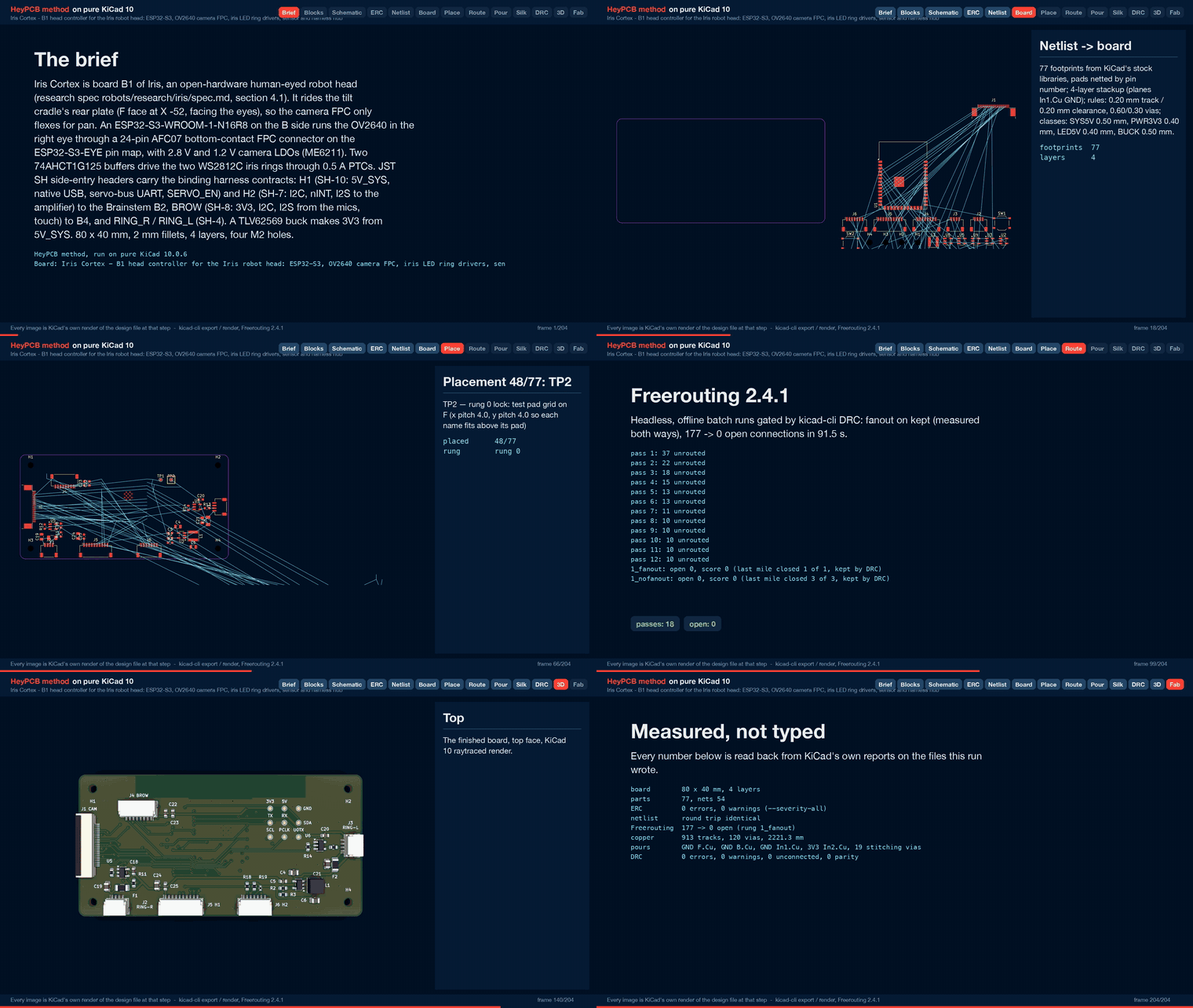
177 → 0 open on rung 1 with fanout. Freerouting left 1 open (CAM_HREF, U1.7 to R10.2); the last-mile router closed it with 4 tracks and no via, and DRC kept it. The no-fanout solve also reached 0 after its last mile. 913 tracks, 101 routing vias, 2221.3 mm: F.Cu 977.3, In2 814.8, B.Cu 429.3. No class narrowed
Pours (only after a measured 0 open)
GND on F.Cu, B.Cu and In1, 3V3 on In2. 19 stitching vias (120 vias in all). 0 open after the pour, after stitching and at the end; 0 island-repair vias
Silkscreen
17 of 17 words and 3 of 3 title lines placed. 40 designators seated, 20 hidden, 3 stitching vias displaced
0 errors. 1 warning: 208 stock-footprint silk strokes at 0.12 mm, which the fab prints at its 0.15 mm minimum
Fab gate
ready, no blockers. 4 copper gerbers; gerber job LayerNumber 4, 1.6 mm. 64 CPL rows (32 top, 32 bottom); the JLC CPL corrected 28 rotations
Media
63 3D frames, the raytraced renders and the design-process video: 1920 x 1080, 139.5 s, 4186 frames (ffprobe)
Timing: the final full run took 4 min 6 s. The route stage took 57.5 s, the renders 154.7 s and the
video 20.1 s.
The same brief routed identically in its last --no-media run before the full run: 913 tracks, 101
vias, 2221.3 mm, DRC 0 / 0 / 0, 0 warnings.
Departures from the spec, and why
J4 (BROW) is 7.6 mm below the top edge, at x 11.95-22.05. The spec zone was x 16-28 at the top
edge.
KiCad's RF_Module:ESP32-S3-WROOM-1 footprint carries Espressif's antenna keep-out: 15 mm
beyond each side of the module, on every copper layer, banning footprints, pads, tracks, vias
and pours. With the module centred, that covers x 16-64, y 0-6.55. No header fits at the top
edge between it and the H1 hole.
J4 still opens upward, toward B4. Its plug rests over bare laminate in that strip.
The mechanism CAD should route the BROW cable up from Z +12.4 over the board face.
The spec's own antenna keep-out (x 31-49, y 0-7) is also in the brief, as a tracks / vias / pour
ban.
The module sits 0.5 mm inside the top edge (its outline spans y 0.50-26.10), not flush.
One PTC per ring. The 5V_LED pin is fed through its own 0.5 A PTC per ring, so the B1 nets are
5V_LED_R and 5V_LED_L. A short in one eye's wires then leaves the other eye lit. The pinout is
unchanged.
Additions the spec does not list:
100 k pull-downs on both buffer inputs, because GPIO47 / GPIO48 float through reset;
33 ohm source resistors on the ring data lines;
10 uF on each 5V_LED;
22 uF + 100 nF on 5V_SYS at J5;
1 uF + 100 nF on 3V3 at J4;
1 uF in and out at each ME6211, per Microne's typical application.
The buffers run from 5V_SYS ahead of the PTCs, so a PTC's drop cannot take them below their 4.5 V
minimum.
Test pads are on the F face, in a 3 x 3 grid right of the module's position. Each pad's name is
printed beside it. A first layout with a column on B, among the camera lines' vias, left 7 of 9
names unplaced.
SDK notes (not changes):
The spec's board fragment spells the keep-out ban "pours". The SDK's word is "pour"; the
brief uses "pour", and "pours" would be refused as bad_keepout.
The fragment's footprints ban over x 31-49, y 0-7 would flag the module itself, so the brief
leaves it to the footprint's own rule area.
The placer's top-edge anchor rung only places at rot 0. KiCad flips a bottom-side part
top-to-bottom, so the module is locked at rot 180 instead.
The placer reads the module's courtyard as its bounding box (x 16-64 with the keep-out). Its
thermal-via pads also make it count as through-hole. So the module's B-face neighbours are
locked by hand.
Assembly notes
Double-sided SMT. The B face carries:
U1, U3 and U4;
BOOT and RESET;
the module's bypass and EN parts;
the FPC's pull-ups, links and decoupling;
the five I2S / MIC_SD resistors next to the module.
The F face carries the connectors, the buck, the ring drivers and the test pads. Check JLC's
placement preview for the bottom side, especially pin 1 of U1 (top right when seen from F).
Camera FPC orientation.
J1 opens to the board's left edge (head -Y), on the F face.
The OV2640 module's FPC comes back from the right eye, bends about Z near B1, and runs +Y along
the F face into J1.
The AFC07 is bottom contact, so insert the FPC with its gold fingers facing the board. Open
the slide lock first and close it after full insertion.
Module pin n lands on pad n. Pad 1 is at the top of J1 (y 14.25, head Z +5.75); pad 24 is at the
bottom.
First power-up check for the camera. With the module inserted, J1 pads 2 (AGND) and 15 (DGND)
must read 0 ohm to GND. If they do not, the FPC is reversed or the module uses the AI-Thinker
ESP32-CAM numbering: map by signal, never by number.
FPC length. Buy the 120 mm class. The spec budgets about 72 mm plus pan slack, and the 75 mm
module is too short.
Image orientation.
Whether the sensor rows run along the FPC exit edge is open question Q2 in the spec. If they do,
correct the image with the OV2640's vflip / hmirror.
If not, rotate the image in firmware. Verify at first light.
DVDD. U4 is fitted for an OV2640 (1.2 V). For an OV3660 / OV5640 module, replace U4 with
ME6211C15M5G-N (C53100) before inserting that module.
Rings. Each ring cable is SH-4 at B1 and four 32 AWG wires soldered to B3 pads P1-P4 (5V_LED,
LED_DIN, GND, GND). J2 is the right eye, J3 the left. The two are interchangeable, and firmware has a
swap flag.
Check before ordering
Re-check stock and class at jlcpcb.com. The pinned rows are live lookups from 2026-10-03. The
lowest stocks are SM04B-SRSS-TB (C160404) at 7,284 and ME6211C28 (C53099) at 15,900.
Buy the camera module first. Confirm its 24-pin pinout against the CAM table, its contact side
and its FPC length (≥ 100 mm overall). Then decide U4's voltage.
Confirm with the mechanism CAD:
the connector positions in the table above, especially J4's lowered position and the BROW cable
path;
the J1 entry from the left edge;
the B-face heights (U1 3.1 mm, buttons 1.5 mm) against the cradle bosses.
Keep the antenna clear. Nothing conductive on the cradle's rear plate over x 16-64, y 0-7 (head
Y -24 to +24, Z +13 to +20). The BROW plug and cable pass at the left end of that strip; check RSSI
on the first board.
Stackup. The board file carries KiCad's derived 4-layer stackup (gerber job: 1.6 mm, 0.48 mm
dielectrics). JLC's real stackup is chosen when ordering. USB and DVP are not impedance-controlled:
USB FS and a 20 MHz DVP clock do not need it over these lengths.
USB ESD sits on B2 (U5 there), not here. A cable plugged straight into H1 from anything but B2
has no protection.
Footprint polarity and orientation in the JLC preview:
U1 pin 1 (on B);
the SOT-23-5 parts;
the SH headers' pin 1 marks.
The CPL was rotation-corrected for 28 parts.
Firmware facts the hardware assumes (spec section 8; not written yet):
GPIO46 must stay low at reset (R7 holds it);
write the VL53L1X to its 2V8 I/O mode;
RMT on GPIO47 / GPIO48 at 800 kHz with a 30 % brightness cap on USB-only power;
SERVO_EN stays low until the INA226 reads VIN ≥ 8.5 V.
No 3D body for J1. KiCad 10.0.6 ships no model for the Jushuo AFC07 footprint, so J1 shows as
bare pads in the renders and has no body in the STEP. Use the catalogue drawing for the 2 mm-tall
housing.
Sources
Facts and URLs only; no datasheet files are stored in this repository.
Iris design spec v0.1 (not published; binding contracts in the Iris system docs): sections 0,
2.8, 3, 4.1, 4.5, 5, 6 and 8. The outline and holes come from its board-outline script and are in board.json.
Part numbers, stock, class and the catalogue facts quoted (PTC resistance, SH and AFC07 heights,
buffer supply range) come from live JLC/LCSC lookups through jlcsearch.tscircuit.com on 2026-10-03.
They are pinned in parts/lcsc_pinned.json with that date.
Pins come from the installed KiCad 10 symbols. Footprints and 3D models are KiCad's stock
libraries.
Licence
SPDX-License-Identifier: CERN-OHL-S-2.0
Copyright 2026 enkhbold470.
This source describes Open Hardware and is licensed under the CERN-OHL-S v2. You may redistribute and
modify this source and make products using it under the terms of the CERN-OHL-S v2
(https://ohwr.org/cern_ohl_s_v2.txt). This source is distributed WITHOUT ANY EXPRESS OR IMPLIED
WARRANTY, INCLUDING OF MERCHANTABILITY, SATISFACTORY QUALITY AND FITNESS FOR A PARTICULAR PURPOSE.
Please see the CERN-OHL-S v2 for applicable conditions.
Source location: boards/iris_cortex/ in the heypcb-kicad repository, with the cortex_* blocks in
blocks/.
The licence covers this board's brief, its cortex_* blocks and the files the pipeline builds from
them. KiCad's symbols, footprints and 3D models are CC-BY-SA-4.0 with the KiCad library exception. The
TS-1187A body in the renders is heypcb-kicad's generated envelope.
Files
board.json is the brief everything is built from.
img/ holds three raytraced renders from the final run: the F face, the B face and an isometric
view.
It measures 80 × 40 mm and has 4 copper layers, 1.6 mm thick.
What parts does the Iris cortex use?
77 parts, built around the ESP32-S3-WROOM-1-N16R8, TLV62569DBVR-TP, SN74AHCT1G125DBVR(UMW) and ME6211C12M5G-N. The full list of its parts is on this page, with links to each part's symbol and footprint where PCBKit's library has them.
Where can I download the Iris cortex KiCad files?
From the HeyPCB/iris-cortex repository on GitHub, at the commit this page was made from: the board is kicad/iris_cortex.kicad_pcb and its schematic kicad/iris_cortex.kicad_sch. PCBKit opens the board in the browser, with nothing to install.
Can I use the Iris cortex design in my own project?
Its repository publishes it under the CERN-OHL-S-2.0 licence: you may reuse it on that licence's terms (keep the author's notice, and for a copyleft licence share your changes alike).
Iris Brainstem: power and servo hub of the Iris robot head. 9 V USB-C PD in, 6 V / 5 A servo rail in stitched copper zones (measured), 5 V rail, half-duplex servo bus with ten ports, speaker amp.
This project transforms a 1998 Furby into an interactive and advanced desktop assistant using a Raspberry Pi W. It incorporates OpenAI and Whisper for natural language processing, primarily relying on Google Cloud Text…
Lightest ESP32-based blimp controller with the works; 9-DoF, ToF altimetry, motor drivers, and Wi-Fi enabled camera streaming, all on a single 300mAh LiPo. >1hr of battery life.