4 layers80 × 40 mm
Iris cortex
HeyPCB/iris-cortex
Iris Cortex: head controller of the Iris robot head. ESP32-S3 (16 MB flash, 8 MB PSRAM), OV2640 eye-camera FPC, iris-ring LED drivers, harness hub.
77 partsCERN-OHL-S-2.0

 Deco025/rtl8367-switch
Five-port gigabit unmanaged Ethernet switch based on the Realtek RTL8367RB - 4-layer KiCad 10 design with fabrication outputs
Rtl8367-switch is an open-source printed circuit board by Deco025, from the Deco025/rtl8367-switch repository on GitHub, published under the CERN-OHL-S-2.0 licence. It is a 4-layer board of 100 × 72 mm with 229 parts on 218 nets, routed with 1,470 tracks and 365 vias.
It is built around the RTL8367RB-VB-CG, TPS54331DDAR and TPS62130ARGTR, with the TPD4E02B04DQAR, AT24C256C-SSHL-T and TPS3808G30DBVR-TP among its other parts. Its parts include 92 resistors, 77 capacitors, 15 ICs, 14 diodes and 7 connectors.


RTL8367RB 五口千兆非网管交换机


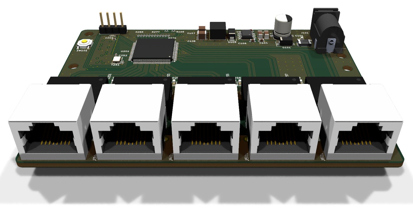
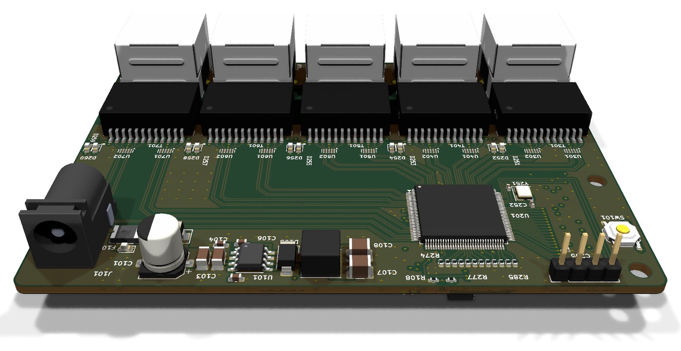
An open-source five-port gigabit Ethernet switch built around the Realtek RTL8367RB. It is unmanaged: the chip boots from strap pins and needs no MCU. Each port has a discrete Pulse H5007NL magnetics module, a shielded RJ45 and two status LEDs. A 12 V input feeds two on-board bucks, 3.3 V (TPS54331) and 1.1 V (TPS62130A). The board is a compact 100 × 72 mm, 4-layer KiCad 10 design, assembled on both sides, with complete fabrication outputs.
| 正面(网口一侧) | 背面(电源一侧) |
|---|---|
 |  |
| 顶层 F.Cu | 底层 B.Cu(从背面看) |
|---|---|
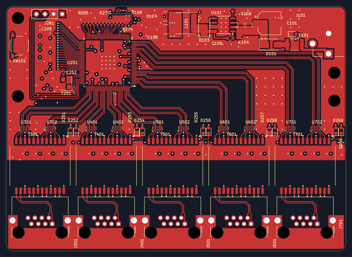 | 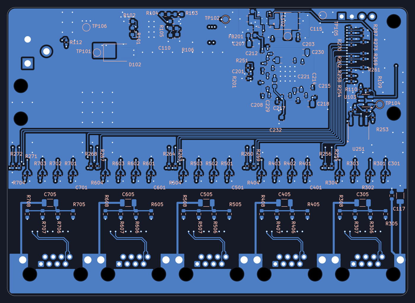 |
第 2 层整层是地,第 3 层是电源分区;图里只画了两个外层。
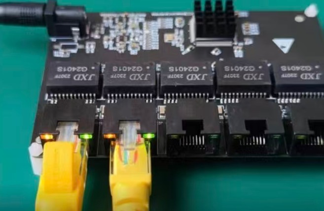
这是本设计的前代样机,已经搭建并通电运行,图中两个网口接线后链路灯亮起。v0.1 在它的基础上重新设计,网络变压器从 JXD G2401S 换成了 Pulse H5007NL。上面的渲染图和走线图都是 v0.1。
| 项 | 值 |
|---|---|
| 交换芯片 | Realtek RTL8367RB-VB-CG(LQFP-128,带散热焊盘) |
| 端口 | 5 × 10/100/1000BASE-T,RJ45 带屏蔽壳 |
| 管理 | 非网管,靠 strap 引脚配置;预留 SMI 调试口(J251)和 EEPROM 位置(默认不贴) |
| 网络变压器 | Pulse H5007NL × 5(每口一颗,分立) |
| 指示灯 | 每口一绿一黄,外加一颗电源灯 |
| 输入 | 12 V DC,5.5 × 2.1 mm 插座(CUI PJ-102AH) |
| 输入保护 | 自恢复保险丝 0.75 A(1812L075/33DR)、防反接肖特基 SS34、TVS SMBJ15A |
| 3.3 V | TPS54331 降压,6.8 µH,SS34 续流 |
| 1.1 V(芯片核心) | TPS62130A 降压,2.2 µH,放在背面,紧靠芯片 |
| 复位 | TPS3808G30 监控 3.3 V,带手动复位按键 |
| 时钟 | 25 MHz 晶体 |
| PCB | 100 × 72 mm,4 层,1.58 mm,嘉立创叠层 JLC04161H-3313A(外层 1 oz,内层 0.5 oz) |
| 装配 | 双面贴片:正面 56 个、背面 129 个,共 185 个 |
flowchart LR
    DC[12 V 输入<br/>保险丝 · 防反接 · TVS] --> B1[TPS54331<br/>3.3 V]
    B1 --> B2[TPS62130A<br/>1.1 V 核心]
    B1 --> FB[磁珠滤波<br/>3.3 V / 1.1 V 模拟与 PLL]
    B1 --> RST[TPS3808<br/>复位监控]
    B2 --> SW
    FB --> SW
    RST --> SW
    X[25 MHz 晶体] --> SW[RTL8367RB<br/>5 口千兆交换]
    SW -- MDI × 4 对 --> T[H5007NL × 5<br/>网络变压器]
    T --> J[RJ45 × 5<br/>Bob Smith 终端到 CHASSIS]
SW --> LED[LED × 10]更完整的说明见 docs/design.md。
.
├── rtl8367-switch.kicad_pro   KiCad 工程
├── *.kicad_sch                原理图:根页 + 电源、芯片供电、芯片控制、5 个网口
├── rtl8367-switch.kicad_pcb   PCB
├── lib/                       工程自带的符号和封装(RTL8367RB、H5007NL、RJ45)
├── fab/                       生产文件(Gerber zip、BOM、坐标、装配图、DRC 报告)
├── 3dmodels/                  第三方 3D 模型的来源清单(模型文件不随仓库分发)
├── docs/
│   ├── design.md              设计说明
│   └── schematics/            原理图 PDF(不装 KiCad 也能看)
├── images/                    渲染图和走线图
├── CHANGELOG.md
└── LICENSE CERN-OHL-S-2.0rtl8367-switch.kicad_pro。RTL8367RB、H5007NL 和 RJ45 的符号与封装在 lib/ 里,工程的库表已经指向它们;其余来自 KiCad 官方库。3dmodels/,3D 查看器(Alt+3)里就能看到完整外观。不下载也不影响原理图、PCB 和生产文件。生产文件已经导出好,坐标原点在板的左上角:
| 用途 | 文件 |
|---|---|
| 上传给板厂 | fab/rtl8367-switch-gerber.zip |
| 物料清单 | fab/rtl8367-switch-bom.csv |
| 贴片坐标(两面) | fab/rtl8367-switch-pos.csv |
| 装配图(第 1 页正面,第 2 页背面镜像) | fab/rtl8367-switch-assembly.pdf |
| 下单参数 | fab/README.md |
下单要点:
详见 docs/design.md。
原理图 ERC 0,PCB DRC 0 错误、0 未连接,原理图与 PCB 一致。装配和调试时请留意:
欢迎提交 Issue 反馈问题或改进建议。
本项目的硬件设计文件(原理图、PCB、生产文件、文档)采用 CERN Open Hardware Licence Version 2 – Strongly Reciprocal (CERN-OHL-S-2.0)。
简单说:可以自由使用、学习、修改、生产和销售;但如果你发布修改后的设计,或者销售基于它的产品,必须用同样的许可证公开对应的设计源文件。
第三方封装、符号和 3D 模型各自遵循其原始许可,不在本许可证范围内。
欢迎通过 Issue 反馈问题或提出改进。
| Qty | Value | Footprint | References |
|---|---|---|---|
| 50 | 100nF | Capacitor_SMD:C_0402_1005Metric | C112, C116, C201, C202, C203, C204, C205, C206, C208, C209, C210, C211, C212, C213, C214, C215 +34 |
| 20 | 0R | Resistor_SMD:R_0402_1005Metric | R301, R302, R303, R304, R401, R402, R403, R404, R501, R502, R503, R504, R601, R602, R603, R604 +4 |
| 20 | 75R | Resistor_SMD:R_0603_1608Metric | R305, R306, R307, R308, R405, R406, R407, R408, R505, R506, R507, R508, R605, R606, R607, R608 +4 |
| 16 | 1k | Resistor_SMD:R_0402_1005Metric | R274, R275, R276, R277, R278, R279, R280, R281, R282, R283, R284, R285, R286, R287, R288, R289 |
| 13 | 4.7k | Resistor_SMD:R_0402_1005Metric | R251, R252, R253, R254, R257, R258, R261, R262, R265, R266, R269, R270, R273 |
| 10 | 470R | Resistor_SMD:R_0402_1005Metric | R255, R256, R259, R260, R263, R264, R267, R268, R271, R272 |
| 10 | TPD4E02B04DQA | Package_SON:USON-10_2.5x1.0mm_P0.5mm | U301, U302, U401, U402, U501, U502, U601, U602, U701, U702 |
| 6 | 1nF | Capacitor_SMD:C_1206_3216Metric | C117, C305, C405, C505, C605, C705 |
| 6 | Green | LED_SMD:LED_0603_1608Metric | D104, D251, D253, D255, D257, D259 |
| 5 | 10uF | Capacitor_SMD:C_0805_2012Metric | C111, C207, C218, C222, C230 |
| 5 | H5007NL | rtl8367-switch:Pulse_H5007NL | T301, T401, T501, T601, T701 |
| 5 | R-RJ45R08P-B000 | rtl8367-switch:RJ45_Ckmtw_R-RJ45R08P-B000_Horizontal | J301, J401, J501, J601, J701 |
| 5 | Yellow | LED_SMD:LED_0603_1608Metric | D252, D254, D256, D258, D260 |
| 4 | 0R | Resistor_SMD:R_0603_1608Metric | FB201, FB202, FB203, R103 |
| 4 | MountingHole | MountingHole:MountingHole_3.2mm_M3 | H1, H2, H3, H4 |
| 2 | 10k | Resistor_SMD:R_0402_1005Metric | R109, R111 |
| 2 | 18pF | Capacitor_SMD:C_0402_1005Metric | C251, C252 |
| 2 | 22nF | Capacitor_SMD:C_0603_1608Metric | C105, C113 |
| 2 | 22uF | Capacitor_SMD:C_0805_2012Metric | C114, C115 |
| 2 | 4.7uF | Capacitor_SMD:C_1206_3216Metric | C102, C103 |
| 2 | 47uF | Capacitor_SMD:C_1210_3225Metric | C107, C108 |
| 2 | GND | TestPoint:TestPoint_Pad_D1.5mm | TP105, TP106 |
| 2 | SS34 | Diode_SMD:D_SMA | D101, D103 |
| 1 | +1V1 | TestPoint:TestPoint_Pad_D1.5mm | TP103 |
| 1 | +3V3 | TestPoint:TestPoint_Pad_D1.5mm | TP102 |
| 1 | 1.5k | Resistor_SMD:R_0402_1005Metric | R112 |
| 1 | 10.2k | Resistor_SMD:R_0603_1608Metric | R104 |
| 1 | 100k | Resistor_SMD:R_0402_1005Metric | R110 |
| 1 | 100nF | Capacitor_SMD:C_0603_1608Metric | C106 |
| 1 | 10nF | Capacitor_SMD:C_0603_1608Metric | C104 |
| 1 | 1812L075/33DR | Fuse:Fuse_1812_4532Metric | F101 |
| 1 | 1M | Resistor_SMD:R_0603_1608Metric | R113 |
| 1 | 1nF | Capacitor_SMD:C_0603_1608Metric | C109 |
| 1 | 1uF | Capacitor_SMD:C_0603_1608Metric | C232 |
| 1 | 2.2uH | Inductor_SMD:L_Sunlord_SWPA4030S | L102 |
| 1 | 2.49k | Resistor_SMD:R_0402_1005Metric | R201 |
| 1 | 25MHz | Crystal:Crystal_SMD_3225-4Pin_3.2x2.5mm | Y251 |
| 1 | 29.4k | Resistor_SMD:R_0603_1608Metric | R106 |
| 1 | 3.24k | Resistor_SMD:R_0603_1608Metric | R105 |
| 1 | 30.1k | Resistor_SMD:R_0402_1005Metric | R107 |
| 1 | 332k | Resistor_SMD:R_0603_1608Metric | R101 |
| 1 | 47pF | Capacitor_SMD:C_0603_1608Metric | C110 |
| 1 | 47uF | Capacitor_SMD:CP_Elec_6.3x7.7 | C101 |
| 1 | 6.8uH | Inductor_SMD:L_Sunlord_SWPA6045S | L101 |
| 1 | 68.1k | Resistor_SMD:R_0603_1608Metric | R102 |
| 1 | 80.6k | Resistor_SMD:R_0402_1005Metric | R108 |
| 1 | AT24C256C | Package_SO:SOIC-8_3.9x4.9mm_P1.27mm | U251 |
| 1 | J_DBG | Connector_PinHeader_2.54mm:PinHeader_1x04_P2.54mm_Vertical | J251 |
| 1 | PJ-102AH | Connector_BarrelJack:BarrelJack_CUI_PJ-102AH_Horizontal | J101 |
| 1 | RESET | Button_Switch_SMD:SW_Push_1P1T_XKB_TS-1187A | SW101 |
| 1 | RTL8367RB-VB-CG | rtl8367-switch:LQFP-128-1EP_14x14mm_P0.4mm_EP5.5x5.5mm_ThermalVias | U201 |
| 1 | SMBJ15A | Diode_SMD:D_SMB | D102 |
| 1 | TPS3808G30DBVR | Package_TO_SOT_SMD:SOT-23-6 | U103 |
| 1 | TPS54331DDA | Package_SO:Texas_HSOP-8-1EP_3.9x4.9mm_P1.27mm_ThermalVias | U101 |
| 1 | TPS62130A | Package_DFN_QFN:VQFN-16-1EP_3x3mm_P0.5mm_EP1.68x1.68mm_ThermalVias | U102 |
| 1 | VIN | TestPoint:TestPoint_Pad_D1.5mm | TP101 |
| 1 | nRESET | TestPoint:TestPoint_Pad_D1.5mm | TP104 |
It measures 100 × 72 mm and has 4 copper layers, 1.58 mm thick.
229 parts, built around the RTL8367RB-VB-CG, TPS54331DDAR, TPS62130ARGTR and TPD4E02B04DQAR. The full list of its parts is on this page, with links to each part's symbol and footprint where PCBKit's library has them.
From the Deco025/rtl8367-switch repository on GitHub, at the commit this page was made from: the board is rtl8367-switch.kicad_pcb and its schematic core_ctrl.kicad_sch. PCBKit opens the board in the browser, with nothing to install.
Its repository publishes it under the CERN-OHL-S-2.0 licence: you may reuse it on that licence's terms (keep the author's notice, and for a copyleft licence share your changes alike).
HeyPCB/iris-cortex
Iris Cortex: head controller of the Iris robot head. ESP32-S3 (16 MB flash, 8 MB PSRAM), OV2640 eye-camera FPC, iris-ring LED drivers, harness hub.

ilomon10/embedded-totalizer-hour-meter
ESP32 engine hour meter & totalizer: firmware, SensorFrame protocol, Node host tools, KiCad PCB and a Deno device simulator


florolf/lab-automation
Plugs into relay and can be used to provide switchable 5V USB power to downstream devices.

Aieda1l/CANsus
Iterated CAN, power, and auxiliary-signal distribution PCB for Newport Robotics Group (Team 948), designed in KiCad.

butchja/esphome-jk-bms-can-PCB
HW platform for https://github.com/Ackmaniac/esphome-jk-bms-can
