

4 layers84 × 66 mm
Spinner
enkhbold470/spinner
12-24 V FOC BLDC motor controller: STM32G431, three IR2104 half bridges with 60 V MOSFETs, MT6701 encoder, CAN FD. 4-layer KiCad 10 board.
87 partsCERN-OHL-S-2.0

 enkhbold470/iron-node
ESP32-S3 industrial gateway: W5500 Ethernet, isolated RS-485 (ADM2587E), CAN, 9-36 V input. 4-layer KiCad 10 board.
Iron node is an open-source printed circuit board by enkhbold470, from the enkhbold470/iron-node repository on GitHub, published under the CERN-OHL-S-2.0 licence. It is a 4-layer board of 90 × 66 mm with 83 parts on 100 nets, routed with 730 tracks and 135 vias.
It is built around the ADM2587EBRWZ-REEL7, ESP32-S3-WROOM-1-N8R8 and SN65HVD230DR, with the USBLC6-2SC6, W5500 and CC0603KRX7R9BB104 among its other parts. Its parts include 34 capacitors, 21 resistors, 7 diodes, 6 ICs and 5 connectors. It belongs with the interfaces and adapters boards and the ESP32 boards of this library.


An ESP32-S3 industrial gateway with Ethernet, isolated RS-485, CAN and a 9-36 V input.
Part of the KiCad projects portfolio. Gerbers are in fab/gerbers/ and zipped in fab/.
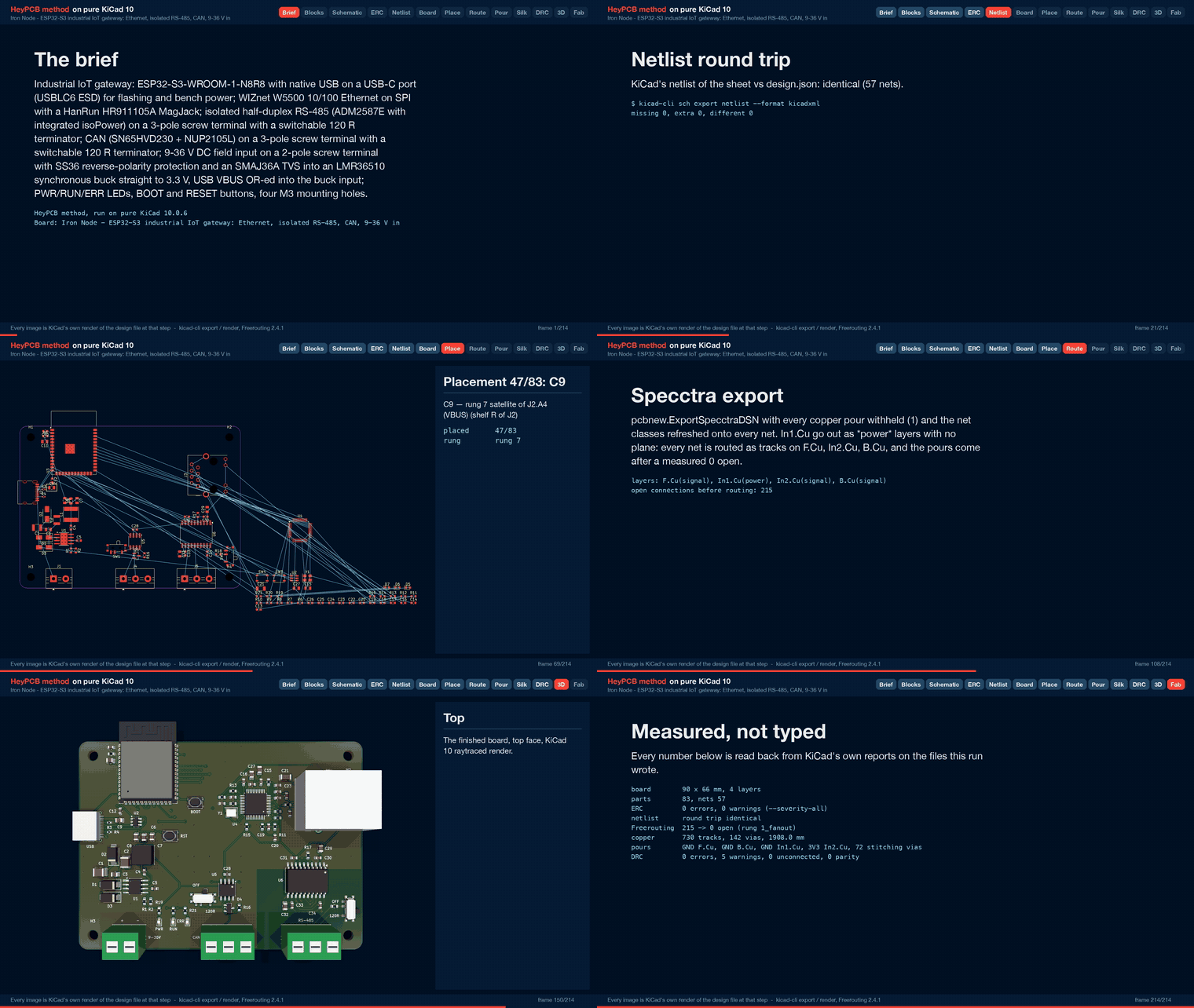
| Layers | Size | Parts | Nets | Connections routed | Vias | ERC errors | DRC errors / unconnected / parity |
|---|---|---|---|---|---|---|---|
| 4 | 90 x 66 mm | 83 | 57 | 215 -> 0 open | 135 | 0 | 0 / 0 / 0 |
Not fabricated, assembled or powered. Every number on this page is measured by KiCad 10 on the files in this folder; the full measurements are in report.json.
| KiCad project | kicad/ |
| Gerbers, BOM, CPL, STEP, schematic PDF | fab/ |
| Renders | top, bottom |
| Design process, every step as KiCad rendered it | media/design-process.mp4 |
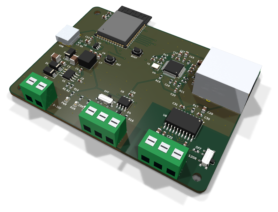
An industrial IoT gateway: an ESP32-S3 with wired Ethernet, isolated RS-485 and CAN, powered
from a 9-36 V DC field supply or from USB-C. It was designed with the HeyPCB method on KiCad 10
(10.0.6), by heypcb-kicad's headless pipeline with Freerouting 2.4.1, from the brief in
board.json.
This board has not been fabricated, assembled or powered. Everything below is what KiCad and the pipeline measured on the design files. Nothing here has been tested on hardware, and nothing here contains or tests firmware.
| Function | GPIO | Module pin |
|---|---|---|
| W5500 SCLK / MOSI / MISO / CS | IO41 / IO40 / IO39 / IO42 | 34 / 33 / 32 / 35 |
| W5500 INTn / RSTn | IO38 / IO2 | 31 / 38 |
| CAN TX / RX (TWAI) | IO9 / IO10 | 17 / 18 |
| RS-485 TX / RX / DE+~RE | IO11 / IO12 / IO13 | 19 / 20 / 21 |
| RUN / ERR LED | IO14 / IO21 | 22 / 23 |
| BOOT | IO0 | 27 |
| USB D- / D+ | IO19 / IO20 | 13 / 14 |
The SPI pins go through the GPIO matrix rather than the FSPI IOMUX pins, because the module's right-side pins face the W5500. IO39-IO42 are the JTAG pins, so JTAG debugging has to go over USB (the S3's built-in USB-JTAG). The strapping pins IO0, IO3, IO45 and IO46 carry nothing except BOOT.
The brief allowed swaps where a chip lacks a KiCad 10 symbol or stock. These were made:
| Asked for | Fitted | Why |
|---|---|---|
| TI ISO1410 + an isolated DC/DC (or an ISOW part) | ADI ADM2587E (ADM2587EBRWZ-REEL7, C12081) | The installed KiCad 10 library has no ISO1410 and no ISOW14xx symbol. TI's ISO3082/ISO3088 have symbols, but the 2026-09-30 JLC lookup found no stock for them. The ADM2587E has a stock symbol and footprint, its own isolated DC/DC, and had 5711 in stock on that date |
| TCAN1044 or SN65HVD230 | SN65HVD230DR (C12084) | The library has no TCAN1044 symbol, only the 14-pin TCAN1043 |
| a stocked TI/MPS synchronous buck to 5 V or 3.3 V, plus an LDO/buck to 3.3 V as needed | LMR36510ADDAR (C1858393) to 3.3 V, no second stage | A 65 V synchronous buck in the library with JLC stock. With USB OR-ed into its input, a single 3.3 V rail serves every chip |
| RJ45 MagJack with integrated magnetics, JLC-stocked, with a KiCad 10 footprint | HanRun HR911105A (C12074) | It has a stock KiCad symbol and footprint |
The pour stage floods the whole outline: GND on F.Cu, In1 and B.Cu, 3V3 on In2. Until this build,
those pours ran under the ADM2587E, between its logic-side and isolated-side pin rows, on all four
layers. On the previous build the isolated copper came within 0.250 mm of them on every layer
(read off that board), and the isolated nets also ran on In2, inside the 3V3 pour. The barrier is now built from the brief's board.keepouts, which become KiCad
rule areas at the board stage. Coordinates are in mm from the board's top-left corner.
iso_barrier_under_u6, x 56.5-90, y 40.5-47.5) bans pours, tracks and
vias on all four layers. It lies between the ADM2587E's two pad rows and runs to the right edge.
The rows' pad edges are at y 40.375 and 47.625, a 7.25 mm land gap (read off the board). The
strip is 7.0 mm wide and leaves 0.125 mm to each row.iso_barrier_down, x 56.5-63.5, y 40.5-66) has the same bans. It runs
from the strip down to the bottom edge, between the CAN and RS-485 terminals. With the board
edges, the strip and the leg close off the bottom-right corner.iso_region_no_pour, x 63.5-90, y 47.5-66, 26.5 x 18.5 mm) bans pours
only. No GND or 3V3 pour enters it on any layer, and the isolated nets route there as tracks.
The rule area is withheld from Freerouting. No stitching via lands there either, because a
stitching via needs GND fill on every GND layer.Read off the board with KiCad 10.0.6's pcbnew on the final kicad/iron_node.kicad_pcb. This
is the minimum edge-to-edge distance between copper of an isolated net and copper of any other
net: pads, plated hole walls, tracks, vias and pour fills. Two methods were used (exact segment
distances, and a bisection on inflated polygons), and they agree.
| Layer | Isolated copper to other copper | Where |
|---|---|---|
| F.Cu | 7.125 mm | ISO_GND pad U6.11 to the GND pour that fills from GND pad U6.10 down to the strip's edge |
| In1.Cu | 8.371 mm | an ISO_GND via at (65.17, 49.59) to the GND plane at the leg's edge |
| In2.Cu | 8.371 mm | the same via to the 3V3 pour at the leg's edge |
| B.Cu | 8.371 mm | the same via to the GND pour at the leg's edge |
| any layer to any layer, in plan view | 7.125 mm | the same F.Cu pair; no copper overlaps across layers |
A full run with media on 2026-10-01 (KiCad 10.0.6, Freerouting 2.4.1). Gate numbers are from
report.json. Anything marked read off the board was measured on kicad/iron_node.kicad_pcb
with KiCad 10.0.6's pcbnew Python module. That file's SHA-256 is the board hash DRC recorded.
| Gate | Result |
|---|---|
| Composition | 83 parts, 57 nets, 43 no-connects (16 block instances of 11 distinct blocks, 5 of them new iron_* blocks) |
| Part binding | 79 of 83 parts bound to an LCSC number, 0 unsourced, 0 identity conflicts. H1-H4, the mounting holes, are not BOM parts. 19 distinct Extended parts, about $57 in JLC loading fees. 3 warnings: R5, R15 and R17 use the 10k 0603 C25804, which had 0 stock at its 2026-06-23 snapshot |
ERC (kicad-cli sch erc --severity-all) | 0 errors, 0 warnings |
| Netlist round trip | identical, 57 nets |
| Routing, rung 1, fanout on | Freerouting left 1 of 215 connections open (VBUS, J2.A9 to C9.1). The last-mile router closed it (3 tracks, 1 via, 0.08 s), and DRC accepted it with no new error. 23.6 s, 70 vias. This solve is kept |
| Routing, rung 1, fanout off | Freerouting left 2 open. The last mile closed VBUS and found no path for ISO_GND (U6.16 to C32.2), so 1 stayed open. 23.0 s, 70 vias |
| Net classes | No class was narrowed. Every track is at its class width (read off the board): PWR 98.4 mm at 0.5 mm, ISO 142.0 mm at 0.2 mm, everything else 1667.7 mm at 0.2 mm |
| Copper | 730 tracks, 1908.0 mm (F.Cu 1058.5, In2 766.2, B.Cu 83.3), 70 routing vias |
| Pours (laid only after a measured 0 open) | GND on F.Cu, In1 and B.Cu, 3V3 on In2, kept out of the barrier and the isolated region. Then 72 stitching vias, 142 vias in total. 0 open after the pours and after stitching, 0 island-repair vias |
| Silkscreen | 16 words placed (see Silkscreen labels below), 47 designators seated and 24 hidden, all 5 back-side title lines placed. The text displaced 7 stitching vias, which leaves 135 vias on the board (read off the board, all 0.6/0.3 mm). 22 footprint silk strokes that left the board or came within 0.3 mm of its edge were dropped |
DRC (kicad-cli pcb drc --severity-all --schematic-parity) | fresh (its board hash matches the final .kicad_pcb), 0 errors, 0 unconnected, 0 parity issues, 5 warnings |
DFM (jlcpcb_4layer profile) | 0 errors, 1 warning: 255 stock-footprint silk strokes at 0.12 mm, which the fab prints at its 0.15 mm minimum |
| Fab gate | ready, no blockers. 4 copper gerbers and a gerber job with LayerNumber 4, 1.6 mm. The JLC CPL corrected 5 rotations |
| 3D, renders, video | all ran: 63 3D frames, then the renders (171.1 s) and the design-process video (214 frames, 146.4 s at 1920 x 1080, measured with ffprobe) |
lib_footprint_mismatch: J1, J4 and J5 (the screw terminals),
J2 (USB-C) and U3 (the module). These are the five footprints that lost silk strokes at the
board edge (read off the board against the library: 5 each on J1, J4 and J5, 4 on U3, 3 on
J2). J1-J5 also carry a generated 3D body from kicad/models/. J3 carries one too and is not
flagged, so the flag follows the dropped strokes.These were measured on runs from 2026-09-30 to 2026-10-01. The reasons are also recorded in
board.json.
silk.polarity puts its mark 1.9-2.3 mm from the pad centre,
which is inside a 2.8 mm terminal pad's own clearance. So it never placed J1's marks. The brief
instead gives J1 a silk.switches entry keyed on each pin's net. That places "+" above pin 1
(VIN_RAW) and "-" above pin 2 (GND), just beyond the terminal's courtyard.The board passes ERC, DRC with schematic parity, DFM and the fab gate in KiCad. It has not been fabricated, assembled or powered.
board.pours takes a
whole inner layer). If EMC or surge testing asks for an ISO_GND plane, add it in KiCad.kicad/models/ are generated from the footprint outline, with the
openings on +y and a 10 mm height envelope, so the renders show the assumption, not a check.
Confirm against MaiXu's drawing that the openings face out of the bottom edge.board.json: the brief. It lists the blocks, net classes, keep-outs, placement targets, routing
and silk settings, each with its reason.report.json: the run's gate report. Every gate number above comes from it.kicad/: iron_node.kicad_pro, iron_node.kicad_sch and the routed, poured
iron_node.kicad_pcb. kicad/models/ holds generated simplified bodies for the USB-C
receptacle, the RJ45 and the 2- and 3-pole MX126 terminals. They are VRML envelopes, not vendor
models.fab/iron_node_gerbers.zip: 11 gerbers (4 of them copper), the gerber job, the drill file
and the drill map.fab/iron_node_bom.csv: the BOM, with MPN and LCSC columns.fab/iron_node_cpl_jlc.csv and fab/iron_node_pos.csv: the JLC CPL and KiCad's position file.
Each lists 75 parts. The through-hole J1, J3, J4 and J5 are not in them.fab/iron_node_schematic.pdf: the schematic.fab/iron_node.step: the 3D model. It has no body for J1-J5, because their generated bodies are
VRML, which the STEP export did not include.media/: hero.png, top.png and bottom.png are KiCad renders, and
design-process.mp4 and design-process.gif show the pipeline's stages. The USB-C, RJ45 and
terminal bodies in the renders are the generated envelopes.In the heypcb-kicad repository, ./run.sh --board boards/iron_node regenerates these outputs
from board.json. The
five blocks written for this board (iron_power_lmr36510, iron_w5500_ethernet,
iron_rs485_adm2587e, iron_can_sn65hvd230 and iron_mounting_hole_m3) give, in their notes,
the symbol pinout each was wired from and the data sheet or reference design its values came from.
| Qty | Value | Footprint | References |
|---|---|---|---|
| 12 | 100nF | Capacitor_SMD:C_0603_1608Metric | C4, C10, C22, C23, C24, C25, C26, C28, C30, C31, C33, C34 |
| 4 | 10uF | Capacitor_SMD:C_0805_2012Metric | C9, C27, C29, C32 |
| 4 | 22uF | Capacitor_SMD:C_0805_2012Metric | C6, C7, C8, C11 |
| 4 | 49.9 | Resistor_SMD:R_0603_1608Metric | R8, R9, R11, R12 |
| 4 | M3 | MountingHole:MountingHole_3.2mm_M3 | H1, H2, H3, H4 |
| 3 | 10k | Resistor_SMD:R_0603_1608Metric | R5, R15, R17 |
| 3 | 1k | Resistor_SMD:R_0603_1608Metric | R19, R20, R21 |
| 2 | 10nF | Capacitor_SMD:C_0603_1608Metric | C16, C20 |
| 2 | 120 | Resistor_SMD:R_0603_1608Metric | R16, R18 |
| 2 | 18pF | Capacitor_SMD:C_0603_1608Metric | C13, C14 |
| 2 | 1uF | Capacitor_SMD:C_0603_1608Metric | C5, C12 |
| 2 | 2.2uF | Capacitor_SMD:C_1210_3225Metric | C1, C2 |
| 2 | 330 | Resistor_SMD:R_0603_1608Metric | R13, R14 |
| 2 | 5.1k | Resistor_SMD:R_0402_1005Metric | R3, R4 |
| 2 | 6.8nF | Capacitor_SMD:C_0603_1608Metric | C18, C19 |
| 2 | PCM12 | Button_Switch_SMD:SW_SPDT_PCM12 | SW1, SW2 |
| 2 | SS36 | Diode_SMD:D_SMA | D1, D3 |
| 1 | 10 | Resistor_SMD:R_0603_1608Metric | R10 |
| 1 | 100nF | Capacitor_SMD:C_0805_2012Metric | C3 |
| 1 | 12.4k | Resistor_SMD:R_0603_1608Metric | R7 |
| 1 | 1M | Resistor_SMD:R_0603_1608Metric | R6 |
| 1 | 1nF | Capacitor_SMD:C_1206_3216Metric | C21 |
| 1 | 20k | Resistor_SMD:R_0603_1608Metric | R2 |
| 1 | 22nF | Capacitor_SMD:C_0603_1608Metric | C17 |
| 1 | 22uH | Inductor_SMD:L_Sunlord_SWPA6045S | L1 |
| 1 | 25MHz | Crystal:Crystal_SMD_3225-4Pin_3.2x2.5mm | Y1 |
| 1 | 4.7uF | Capacitor_SMD:C_0805_2012Metric | C15 |
| 1 | 47k | Resistor_SMD:R_0603_1608Metric | R1 |
| 1 | 9-36V IN | TerminalBlock:TerminalBlock_MaiXu_MX126-5.0-02P_1x02_P5.00mm | J1 |
| 1 | ADM2587EBRWZ | Package_SO:SOIC-20W_7.5x12.8mm_P1.27mm | U6 |
| 1 | BOOT | Button_Switch_SMD:SW_SPST_PTS810 | SW3 |
| 1 | CAN | TerminalBlock:TerminalBlock_MaiXu_MX126-5.0-03P_1x03_P5.00mm | J4 |
| 1 | ESP32-S3-WROOM-1-N8R8 | RF_Module:ESP32-S3-WROOM-1 | U3 |
| 1 | HR911105A | Connector_RJ:RJ45_Hanrun_HR911105A_Horizontal | J3 |
| 1 | LMR36510ADDAR | Package_SO:Texas_HTSOP-8-1EP_3.9x4.9mm_P1.27mm_EP2.95x4.9mm_Mask2.4x3.1mm_ThermalVias | U1 |
| 1 | NUP2105L | Package_TO_SOT_SMD:SOT-23 | D4 |
| 1 | Orange (RUN) | LED_SMD:LED_0603_1608Metric | D6 |
| 1 | RESET | Button_Switch_SMD:SW_SPST_PTS810 | SW4 |
| 1 | RS-485 | TerminalBlock:TerminalBlock_MaiXu_MX126-5.0-03P_1x03_P5.00mm | J5 |
| 1 | Red (ERR) | LED_SMD:LED_0603_1608Metric | D7 |
| 1 | Red (PWR) | LED_SMD:LED_0603_1608Metric | D5 |
| 1 | SMAJ36A | Diode_SMD:D_SMA | D2 |
| 1 | SN65HVD230DR | Package_SO:SOIC-8_3.9x4.9mm_P1.27mm | U5 |
| 1 | USB-C | Connector_USB:USB_C_Receptacle_HRO_TYPE-C-31-M-12 | J2 |
| 1 | USBLC6-2SC6 | Package_TO_SOT_SMD:SOT-23-6 | U2 |
| 1 | W5500 | Package_QFP:LQFP-48_7x7mm_P0.5mm | U4 |
It measures 90 × 66 mm and has 4 copper layers, 1.6 mm thick.
83 parts, built around the ADM2587EBRWZ-REEL7, ESP32-S3-WROOM-1-N8R8, SN65HVD230DR and USBLC6-2SC6. The full list of its parts is on this page, with links to each part's symbol and footprint where PCBKit's library has them.
From the enkhbold470/iron-node repository on GitHub, at the commit this page was made from: the board is kicad/iron_node.kicad_pcb and its schematic kicad/iron_node.kicad_sch. PCBKit opens the board in the browser, with nothing to install.
Its repository publishes it under the CERN-OHL-S-2.0 licence: you may reuse it on that licence's terms (keep the author's notice, and for a copyleft licence share your changes alike).
enkhbold470/spinner
12-24 V FOC BLDC motor controller: STM32G431, three IR2104 half bridges with 60 V MOSFETs, MT6701 encoder, CAN FD. 4-layer KiCad 10 board.

HeyPCB/quack-core
Brain board for the Open Duck Mini: Pi Zero 2W carrier, 14-servo STS bus, fused 2S power path in stitched copper zones (15-18 A battery side), USB-C charging with balancing, IMU.

mahmoud-elghamry/thermocouple
This directory is a self-contained KiCad 10 project. It does not share files with, and must not be confused with, the single-channel board in hardware/single-channel/.

enkhbold470/ice-core
iCE40UP5K FPGA board with 8 MB PSRAM and three Pmods, programmed over USB-C by an RP2040. 6-layer KiCad 10 board.

CappyT/freedo
Local coordinator for tado V3+ heating devices, with a Home Assistant integration and add-on


jgrano/Nx-PCBA
Install all of these before opening the project:

techmannih/pd1180-epr
PD1180-EPR — NEMA 34 Smart Motor-Mounted Stepper Controller with USB-C PD 3.1 EPR