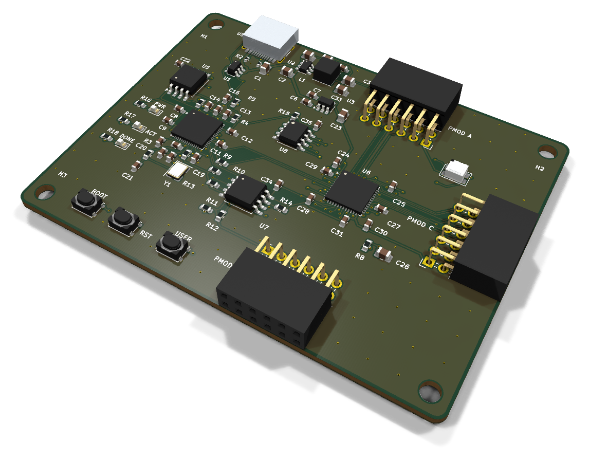
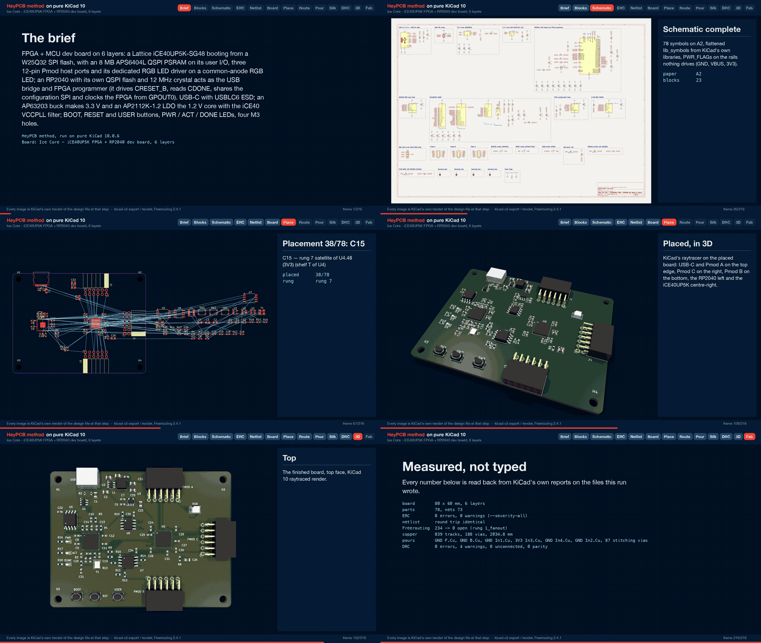
Ice core is an open-source printed circuit board by enkhbold470, from the enkhbold470/ice-core repository on GitHub, published under the CERN-OHL-S-2.0 licence. It is a 6-layer board of 80 × 60 mm with 78 parts on 99 nets, routed with 839 tracks and 180 vias.
It is built around the RP2040, ICE40UP5K-SG48I and W25Q32JVSSIQ, with the AP63203WU, AP2112K-1.2TRG1 and APS6404L-3SQR-SN among its other parts. Its parts include 35 capacitors, 18 resistors, 8 ICs, 4 diodes and 4 connectors. It belongs with the fPGA and programmable logic boards and the RP2040 and FPGA and CPLD boards of this library.
Not fabricated, assembled or powered. Every number on this page is measured by KiCad 10 on the files in this folder; the full measurements are in report.json.
Ice Core is an FPGA board: a Lattice iCE40UP5K with 8 MB of QSPI PSRAM and three
Pmod host ports, programmed and clocked over USB-C by an RP2040, on 80 x 60 mm of
6-layer board. It was designed with the HeyPCB method on KiCad 10 (the headless
heypcb-kicad pipeline, routed by Freerouting 2.4.1) from the brief in board.json.
This board has not been fabricated, assembled or powered. It passes ERC, the
netlist round trip, routing, DRC with schematic parity, DFM and the fab gate in
KiCad 10.0.6, headless, and nothing more. No firmware or gateware for it exists.
Every gate number below is read from report.json. The stackup, the vias in the
exposed pads, the pours, part positions, pad nets, via counts and spacing, the
silkscreen and each footprint's 3D model were read from kicad/ice_core.kicad_pcb
with KiCad 10.0.6's pcbnew.
What it is
FPGA
Lattice iCE40UP5K-SG48 (QFN-48), booting from a W25Q32JV 4 MB SPI flash in controller mode
FPGA memory
AP Memory APS6404L-3SQR-SN, 8 MB QSPI pseudo-SRAM (SOIC-8), on six FPGA I/O
MCU
Raspberry Pi RP2040 (QFN-56) with its own W25Q32JV 4 MB QSPI boot flash and the ABM8-272-T3 12 MHz crystal
MCU role
USB bridge and FPGA programmer: drives CRESET_B, reads CDONE, owns the configuration SPI, clocks the FPGA from GPOUT0
USB
USB-C receptacle (HRO TYPE-C-31-M-12), 5.1k CC pull-downs, USBLC6-2SC6 ESD clamp, 27 ohm series terminations at the RP2040
3.3 V
Diodes AP63203WU buck from VBUS, 2 A, 3.9 uH
1.2 V
AP2112K-1.2 LDO from VBUS, so the FPGA core rises before its 3.3 V banks; VCCPLL through a 100 ohm / 4.7 uF / 100 nF filter
I/O
three 12-pin Pmod host ports (2x6 right-angle sockets) on the FPGA, 8 signals each
UI
common-anode RGB LED on the iCE40's RGB driver; BOOT, RESET (RP2040) and USER (FPGA) buttons; PWR, ACT and DONE LEDs
Mechanical
80 x 60 mm, 2 mm corner radius, four M3 holes (3.2 mm)
Stackup
6 copper layers (below)
Connections that firmware and gateware need
RP2040 (pin numbers and names from the KiCad symbol, read back from the run's
netlist):
RP2040
pin
net
use
GPIO16
27
CFG_CIPO
SPI0 RX: flash DO and the FPGA's SPI_SI
GPIO17
28
CFG_SS
SPI0 CSn: flash /CS and the FPGA's SPI_SS_B (10k pull-up)
GPIO18
29
CFG_SCK
SPI0 SCK (10k pull-up)
GPIO19
30
CFG_COPI
SPI0 TX: flash DI and the FPGA's SPI_SO
GPIO20
31
FPGA_CRESET
CRESET_B (10k pull-up)
GPIO21
32
FPGA_CLK
GPOUT0 into the iCE40's global buffer pin 35 (IOT_46b_G0)
GPIO22
34
FPGA_CDONE
CDONE (10k pull-up)
GPIO24
36
LED_DONE
DONE LED (firmware mirrors CDONE)
GPIO25
37
LED_ACT
ACT LED
QSPI_*
51-56
QSPI_*
boot flash
USB_DM / USB_DP
46 / 47
via 27 ohm
USB-C
iCE40UP5K-SG48 (package pin numbers; every one except RGB0-2 is an IO* pin of
the KiCad symbol):
function
pins
PSRAM CE#, SCLK, SIO0, SIO1, SIO2, SIO3
3, 4, 6, 9, 10, 11
Pmod A pins 1-4 / 7-10
2, 47, 45, 43 / 48, 46, 44, 42
Pmod B pins 1-4 / 7-10
25, 21, 19, 13 / 26, 23, 20, 18
Pmod C pins 1-4 / 7-10
38, 36, 32, 28 / 37, 34, 31, 27
clock in (from RP2040 GPOUT0)
35 (G0)
USER button (to GND, enable the pull-up in gateware)
12
RGB0 / RGB1 / RGB2
39 red / 40 green / 41 blue cathode
configuration SPI SO / SCK / SS / SI
14 / 15 / 16 / 17
The pin plan: the symbol has 36 IO* pins, 4 of them the configuration SPI, which
leaves 32 general I/O, and this board uses all 32. Each Pmod takes the I/O on the
side of the FPGA it faces and its missing pins from the next corner
counter-clockwise (Pmod B from the bottom of the right side, Pmod C from the right
end of the top, Pmod A from the top of the left side), so no Pmod crosses the
configuration SPI at the bottom-left corner. An earlier plan crossed it with Pmod B
and left PB8 open at pin 11. Pmod order along each connector follows the pin order
along the FPGA's edge.
Pmod pin numbers are Digilent's (Pmod Interface Specification 1.1.0, Figure 5).
On KiCad's PinSocket_2x06_P2.54mm_Horizontal they land as Pmod pin 1 -> pad 11,
2 -> 9, 3 -> 7, 4 -> 5, 5 (GND) -> 3, 6 (3V3) -> 1, 7 -> 12, 8 -> 10, 9 -> 8,
10 -> 6, 11 (GND) -> 4, 12 (3V3) -> 2: the footprint's square pad 1 is Pmod pin 6.
Stackup
pcbnew reads 6 copper layers and a 1.6 mm board from the board file. The file holds
no stackup section, so this is KiCad's default 6-layer stackup, not a fab's: choose
the fab's own 6-layer stackup when ordering. pcbnew's stackup object is not
scriptable in KiCad 10.0.6, so the layer thicknesses below come from the gerber job
file (ice_core-job.gbrjob in fab/ice_core_gerbers.zip). Nothing on this board
is impedance controlled (USB runs at Full Speed).
layer
role while routing
pour after routing
filled as
copper
F.Cu
signal
GND
12 pieces
0.035 mm
In1.Cu
GND plane
GND
1 piece
0.035 mm
In2.Cu
signal
GND
2 pieces
0.035 mm
In3.Cu
power plane
3V3, zone priority 1
1 piece
0.035 mm
In4.Cu
GND plane
GND
1 piece
0.035 mm
B.Cu
signal
GND
1 piece
0.035 mm
In3.Cu is auto in the brief: the supply rail with at least 1.5x the pins of the
next one. In this run's netlist 3V3 has 54 pins and no other supply more than 12
(VBUS). Five FR4 dielectrics of 0.274 mm, 1.6 mm overall.
Why this plan: every routed layer sits next to a plane (F.Cu over In1, In2 between
In1 and In3, B.Cu over In4), so every signal has its return path beside it, and
In3/In4 are a tightly coupled power/ground pair. Each of the three planes fills as
one piece. The pieces are counted on the fill stored in the board file. The silk
stage removed 8 stitching vias after that fill, and refilling a copy of the board
gave the same counts on every layer. The price is routing room: Freerouting routes
on F.Cu, In2.Cu and B.Cu only, the same three layers as on a 4-layer board.
Measured gates
One full run with media, 2026-10-01: KiCad 10.0.6 (from the DRC report),
Freerouting 2.4.1 (from its log). The Specctra export carried the brief's 0.5 mm
hole-to-hole minimum to Freerouting as a 0.3 mm via_via clearance
(viaViaClearance_mm in the report: 0.5 mm + 0.3 mm drill - 0.5 mm via).
74 bound, 0 unsourced, 0 conflicts; H1-H4 not in the BOM; 17 Extended part numbers, $51.0 estimated JLC Extended fees
ERC
0 errors, 0 warnings
Netlist round trip
identical, 73 nets
Route
234 -> 0 open. Fanout solve kept: 0 open, DRC score 0, 101 vias. Fanout-off solve: 2 open (PSRAM_CS, U4_RP_DM), and the last mile closed neither (U4_RP_DM hit its 400,000-expansion search cap, PSRAM_CS had no path). 2 locked vias in exposed pads (U4.57, U6.49). 839 tracks, 2034.8 mm (F.Cu 1180.9, In2.Cu 644.1, B.Cu 209.8)
Pours
GND on F.Cu, B.Cu, In1.Cu, In4.Cu, In2.Cu; 3V3 on In3.Cu; 87 stitching vias, 0 island-repair vias; 0 open after the pours, after stitching and at the end; 188 vias after the pours
Silkscreen
11 of 11 words in place of designators; 55 designators seated, 12 hidden where nothing fit; all 4 title lines placed, on the back; 8 GND stitching vias displaced under text; 90 footprint silk items clipped at the board edge (29 on each Pmod socket J2-J4, 3 on the USB-C J1)
DRC (fresh, schematic parity)
0 errors, 0 unconnected, 0 parity; 4 warnings, all lib_footprint_mismatch, on J1-J4, the four footprints whose silk was clipped; no repairs
DFM (jlcpcb_6layer)
0 errors, 1 warning: stock footprint silk down to 0.10 mm (292 items), printed at the fab's 0.15 mm
Fab
ready, no blockers; 6 copper gerbers (F, In1, In2, In3, In4, B) and a gerber job with LayerNumber 6 and a 1.6 mm board; drill, BOM, CPL (6 rotations corrected), schematic PDF, STEP
Media
all ran: 63 3D frames, then the raytraced renders and the design-process video (216 frames; 150.0 s at 1920 x 1080, measured with ffprobe)
Vias, measured on the finished board: 180 in all. 101 are routed vias at 0.5/0.3 mm,
2 of them the locked vias in the exposed pads. 79 are stitching vias at 0.6/0.3 mm:
87 laid by the pour stage, less the 8 the silkscreen displaced. The closest two via
holes are 0.507 mm apart (PB10 and PB3), and no pair is under the 0.5 mm minimum.
DRC reports no hole_to_hole rows.
Silkscreen
The front carries a word instead of a designator on the 11 parts a user plugs into,
presses or reads: USB, PMOD A, PMOD B, PMOD C, BOOT, RST, USER, PWR, ACT, DONE and
RGB.
The board's name is on the back: all four title lines ("Ice Core", "iCE40UP5K +
RP2040, 6 layers", "rev A heypcb-kicad", "pure KiCad 10 + Freerouting"), placed as
one block. The brief asks for the block on the board's centre line, 22 mm from the
top edge. That spot was not free, so the block landed 9 mm left and 3 mm down, at
x 19.9-42.1 mm and y 23.5-32.9 mm from the board's top-left corner, behind the
RP2040's right side and the PSRAM. The previous full run, the one this README
described before, placed none of the four lines, because the 5 mm stitching-via
grid left no gap long enough. Text may now displace a GND stitching via. This run
displaced 8: 4 under the title and 4 under the ACT, BOOT, USER and PMOD A words.
Files
board.json: the brief the pipeline built everything here from.
report.json: the run's gate report, the source of every number above.
kicad/: ice_core.kicad_pro, ice_core.kicad_sch, ice_core.kicad_pcb
(routed and poured) and models/, the two generated 3D envelopes (D1 and J1,
below).
fab/ice_core_gerbers.zip: 13 layer gerbers, the gerber job, the drill file
and the drill map.
fab/ice_core_bom.csv, fab/ice_core_cpl_jlc.csv (JLC placement, rotations
corrected), fab/ice_core_pos.csv (KiCad placement),
fab/ice_core_schematic.pdf, fab/ice_core.step (72 bodies; none for D1, J1
or the mounting holes).
media/: hero.png, top.png, bottom.png and the design-process video
(design-process.mp4, design-process.gif).
3D models
KiCad 10.0.6 installs no 3D model for three of the footprints this board uses,
so the pipeline gives each a stand-in (read from each footprint's model path on
the board):
U6, the iCE40 (QFN-48-1EP_7x7mm_P0.5mm_EP5.6x5.6mm) uses the library's
QFN-48-1EP_7x7mm_P0.5mm_EP5.15x5.15mm.step. It is the same 7 x 7 mm body
with the same 48 pins. Only the exposed pad differs, and the body hides it.
fab/ice_core.step carries this body.
D1, the RGB LED (LED_Avago_PLCC4_3.2x2.8mm_CW) is a simplified envelope
that the pipeline generates (kicad/models/led_plcc4_3.2x2.8.wrl): a white
3.2 x 2.8 mm body with a clear lens and a dark mark at the pad-1 corner. Its
1.9 mm height is an assumption. It is not the TuoZhan part's model.
J1, the USB-C receptacle is also a generated envelope
(kicad/models/usb_c_hro_type-c-31-m-12.wrl).
Both envelopes are VRML files. They show in the renders, but fab/ice_core.step
has no body for D1 or J1.
Parts that are not what the request named
iCE40UP5K-SG48I (LCSC C2678152), the tray part, on KiCad's
FPGA_Lattice:ICE40UP5K-SG48ITR symbol (tape and reel): same die, same QFN-48.
LCSC stocks only the tray part.
W25Q32JVSSIQ (C179173) as the RP2040's boot flash, where Raspberry Pi's
minimal design uses a W25Q128JVS. The RP2040's boot2_w25q080 second stage
drives any W25Q part in quad-I/O mode; this one holds 4 MB. It is the same
part as the FPGA's configuration flash.
RGB LED: TuoZhan S4-3528RGBTA-A (C2827321) on KiCad's
LED_Avago_PLCC4_3.2x2.8mm_CW footprint with the Device:LED_BGRA symbol.
KiCad's Broadcom ASMB-MTB0/MTB1 symbols carry their own footprint, but LCSC
lists neither part. The part's data sheet numbers its pins 1 blue cathode,
2 anode, 3 green cathode, 4 red cathode. With its pin 1 on pad 1, the footprint's
pads 1-4 carry blue, green and red cathode and the anode (on the board: LED_B,
LED_G, LED_R, 3V3), which is Device:LED_BGRA. The part's own pins 2-4 are not
the pad numbers.
10k resistors: FRC0603F1002TS (C2906982, Extended) instead of the Basic
C25804 the pinned table offers: that one had 0 stock and is no longer in the
live catalogue (2026-09-30).
Part numbers come from heypcb-kicad's pinned LCSC table. Of the 28 distinct LCSC
numbers in fab/ice_core_bom.csv, 14 carry a live lookup dated 2026-09-30 and 14
older snapshots (2026-06-23 to 2026-07-03), so check stock when ordering. The
APS6404L-3SQR-SN (C5333729) had 41 in stock at its lookup.
Check before ordering
It has never been built. Order one panel, assemble one board, and bring
it up rail by rail (VBUS, 3.3 V, 1.2 V) before trusting anything else.
Stackup. The board file states none, so the gerber job carries KiCad's
default. Replace it with the fab's 6-layer stackup.
Vias in the exposed pads. One locked 0.5/0.3 mm GND via sits at the centre
of each exposed pad: the RP2040's (U4.57, 3.2 x 3.2 mm) and the iCE40's
(U6.49, 5.6 x 5.6 mm). The board asks for no filling and no capping. On top
each via lies inside the pad's solder-mask opening, an open hole, and the
paste windows (4 on U4, 16 on U6) leave it uncovered. Ask for filled and capped
vias, or expect solder to wick into them.
RGB LED orientation and land pattern. The S4-3528RGBTA-A's recommended
pads (1.8 x 0.8 mm, 1.6 mm apart, from its data sheet) lie only roughly inside
the Avago footprint's (1.5 x 1.1 mm at 3.0 x 1.5 mm pitch, measured on D1).
Check pin 1 and the paste in the assembler's preview.
VCCPLL filter. The 100 nF (C27) sits at pin 29: its VCCPLL pad centre is
1.84 mm from the pin's. The 100 ohm (R8) and the 4.7 uF (C26) sit below-right of the
FPGA, at (57.25, 38.50) mm and (60.50, 39.00) mm from the board's top-left,
8.6 and 10.9 mm from pin 29, out of Pmod C's escape. U6_VCCPLL runs 15.8 mm
of track (F.Cu 7.0, In2.Cu 8.8) through 2 vias. Move them closer if you can
route it.
VPP_2V5 runs from 3.3 V (pin 24 is on the 3V3 net). Fine for booting from
flash and for the RGB driver; never program the iCE40's NVCM from this rail.
Firmware has to do the board's job: start GPOUT0 (the FPGA's only clock),
hold CRESET_B low while it writes the configuration flash, then release the
SPI pins (tri-state) before releasing CRESET_B, since the FPGA reads the same
flash as an SPI controller.
Extended parts: 17 Extended part numbers, about $51 in JLC's per-part
Extended fees at the report's estimate.
Reproduce
From the heypcb-kicad repository:
bash
./run.sh --board boards/ice_core              # with the 3D renders and the video
./run.sh --board boards/ice_core --no-media   # the gates only
Placement walks parts in reference order and the Specctra file is written in a
content-only order, so the brief is meant to route the same way every time. This
README reports one run. The previous full run, made before the silkscreen and
3D-model changes, reported the same route: 234 -> 0 open, 101 vias, 839 tracks and
2034.8 mm. An earlier run without media also gave 234 -> 0 open with 101 vias. The
boards were not compared track by track.
It measures 80 × 60 mm and has 6 copper layers, 1.6 mm thick.
What parts does the Ice core use?
78 parts, built around the RP2040, ICE40UP5K-SG48I, W25Q32JVSSIQ and AP63203WU. The full list of its parts is on this page, with links to each part's symbol and footprint where PCBKit's library has them.
Where can I download the Ice core KiCad files?
From the enkhbold470/ice-core repository on GitHub, at the commit this page was made from: the board is kicad/ice_core.kicad_pcb and its schematic kicad/ice_core.kicad_sch. PCBKit opens the board in the browser, with nothing to install.
Can I use the Ice core design in my own project?
Its repository publishes it under the CERN-OHL-S-2.0 licence: you may reuse it on that licence's terms (keep the author's notice, and for a copyleft licence share your changes alike).
Brain board for the Open Duck Mini: Pi Zero 2W carrier, 14-servo STS bus, fused 2S power path in stitched copper zones (15-18 A battery side), USB-C charging with balancing, IMU.
Iris Brainstem: power and servo hub of the Iris robot head. 9 V USB-C PD in, 6 V / 5 A servo rail in stitched copper zones (measured), 5 V rail, half-duplex servo bus with ten ports, speaker amp.