

4 layers90 × 66 mm
Iron node
enkhbold470/iron-node
ESP32-S3 industrial gateway: W5500 Ethernet, isolated RS-485 (ADM2587E), CAN, 9-36 V input. 4-layer KiCad 10 board.
83 partsCERN-OHL-S-2.0

 enkhbold470/spinner
12-24 V FOC BLDC motor controller: STM32G431, three IR2104 half bridges with 60 V MOSFETs, MT6701 encoder, CAN FD. 4-layer KiCad 10 board.
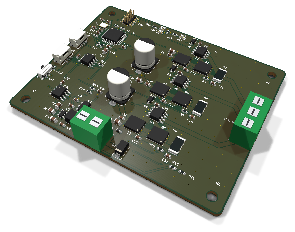
Spinner is an open-source printed circuit board by enkhbold470, from the enkhbold470/spinner repository on GitHub, published under the CERN-OHL-S-2.0 licence. It is a 4-layer board of 84 × 66 mm with 87 parts on 62 nets, routed with 734 tracks and 167 vias.
It is built around the STM32G431KBT6, TCAN332GD and IR2104STRPBF, with the AP63203WU, MT6701CT-STD and L78L12ABUTR-CN among its other parts. Its parts include 34 capacitors, 18 resistors, 8 ICs, 7 diodes and 6 transistors. It belongs with the robots and motor control and interfaces and adapters boards and the STM32 boards of this library.


A 12-24 V field-oriented-control BLDC motor controller: STM32G431, three IR2104 half bridges, MT6701 encoder, CAN FD.
Part of the KiCad projects portfolio. Gerbers are in fab/gerbers/ and zipped in fab/.
| Layers | Size | Parts | Nets | Connections routed | Vias | ERC errors | DRC errors / unconnected / parity |
|---|---|---|---|---|---|---|---|
| 4 | 84 x 66 mm | 87 | 52 | 205 -> 0 open | 167 | 0 | 0 / 0 / 0 |
Not fabricated, assembled or powered. Every number on this page is measured by KiCad 10 on the files in this folder; the full measurements are in report.json.
| KiCad project | kicad/ |
| Gerbers, BOM, CPL, STEP, schematic PDF | fab/ |
| Renders | top, bottom |
| Design process, every step as KiCad rendered it | media/design-process.mp4 |
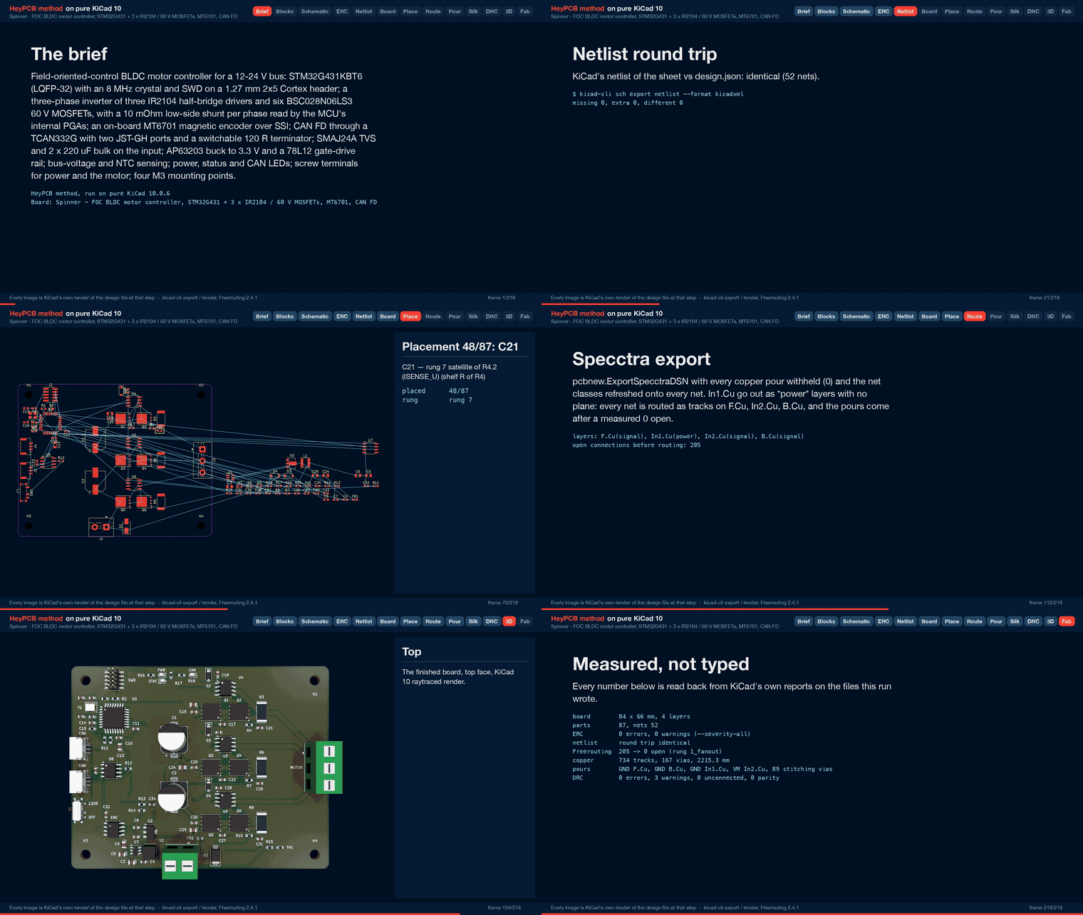
Spinner is a field-oriented-control (FOC) controller for a three-phase BLDC motor on a 12-24 V
bus. An STM32G431 drives three IR2104 half bridges and six 60 V MOSFETs, reads low-side shunts
through its own PGAs, and has an MT6701 magnetic encoder and CAN FD on the board. It was designed
with the HeyPCB method on KiCad 10 (the headless heypcb-kicad pipeline, routed by Freerouting
2.4.1) from the brief in board.json.
It has not been fabricated, assembled or powered. It carries no firmware. FOC firmware, such
as SimpleFOC or ST's MCSDK, is a separate project, and so are the timer, PGA and ADC settings that
the sense path below needs. Every gate number below is read from report.json. What this README
says about specific nets, pours, pads and silkscreen was read from kicad/spinner.kicad_pcb with
KiCad 10.0.6's pcbnew.
| Asked for | On the board | Why |
|---|---|---|
| DRV8316 (integrated FETs and current sense) | 3 x IR2104 + 6 x BSC028N06LS3, plus three 10 mOhm low-side shunts read by the MCU's PGAs | KiCad 10 has no DRV8316 symbol. The integrated three-phase stages it does have are not workable here. The DRV8311 is rated for a 3-20 V supply. The MP6536DU operates at 26 V (28 V absolute maximum, MPS datasheet). Both are 0.4 mm-pitch QFNs whose single 0.2 mm pins cannot take a current-rated track: this pipeline runs Freerouting without neck-down, so a net's class width has to fit every pad on that net. Discrete MOSFETs carry the 1.5 mm motor class on F.Cu end to end. |
| TCAN1044 | TCAN332G (TCAN332GDR) | KiCad 10 has no TCAN1044 symbol. The TCAN332G is in Interface_CAN_LIN, runs CAN FD up to 5 Mbps, and runs from 3.3 V, so the board needs no 5 V rail. |
| STM32G431, LQFP-48 or LQFP-32 | STM32G431KBT6, LQFP-32 | Its 0.8 mm pitch is easier to route. Each function below was read from the symbol's own pin alternates. With the HSE crystal on PF0/PF1, TIM1's three complementary outputs do not all fit this package, so the inverter uses one PWM per phase and the IR2104's internal dead time. |
The MCU pins used (pin names read back from the run's netlist):
| Pin | Net | Function |
|---|---|---|
| PA8 / PA9 / PA10 | PWM_U / PWM_V / PWM_W | TIM1_CH1 / CH2 / CH3 |
| PB5 | DRV_EN | IR2104 ~SD (all three), 100k pull-down. PA15 and PB4 come out of reset with JTAG pull-ups, so neither is used here |
| PA1 / PA7 / PB0 | ISENSE_U / V / W | OPAMP1_VINP / OPAMP2_VINP / OPAMP3_VINP |
| PA0 | VM_SENSE | ADC1_IN1 |
| PA3 | TEMP | ADC1_IN4 |
| PA4 / PA5 / PA6 | ENC_CS / ENC_CLK / ENC_DO | SPI1_NSS / SCK / MISO to the MT6701 (Z/CSN, B/CLK, A/DO) |
| PB4 | ENC_MODE | MT6701 MODE (its 200k pull-up holds it high in reset) |
| PA11 / PA12 | CAN_RX / CAN_TX | FDCAN1 |
| PA13 / PA14 / PB3 / NRST | SWD | SWDIO / SWCLK / SWO / reset |
| PA15 / PB6 | LED_STAT / LED_CAN | red / orange LEDs (the green PWR LED is on 3V3) |
| PB8 | BOOT0 | 4.7k pull-down: boots from flash |
report.json)| Gate | Result |
|---|---|
| Composition | 16 block instances → 87 parts, 52 nets, 10 no-connects |
Part binding (lcsc_pinned.json) | 83 of 87 parts bound to an LCSC number, 0 unsourced, 0 identity conflicts. The four mounting holes (H1-H4) are not in the BOM: there is nothing to buy. 20 distinct Extended parts, about $60 in JLC loading fees |
ERC (kicad-cli sch erc --severity-all) | 0 errors, 0 warnings |
| Netlist round trip | identical, 52 nets |
| Freerouting, rung 1, fanout on (kept) | 205 → 0 open in 12.4 s, DRC score 0, 78 vias |
| Freerouting, rung 1, fanout off (measured for comparison) | 205 → 0 open in 10.8 s, DRC score 0, 80 vias. On a tie the first solve is kept. Neither solve needed the last-mile router |
| Copper | 734 tracks, 78 routing vias, 2215.3 mm of track (F.Cu 1357.9, In2 754.5, B.Cu 102.8). No class was narrowed: VMBUS and MOTOR stayed at 1.5 mm. After the import, 29 segments were widened to their class width; one 2.54 mm GND segment at the SWD header stays at the 0.15 mm board minimum, because 0.2 mm would not clear |
| Pours (only after a measured 0 open) | GND on F.Cu, In1 and B.Cu; VM on In2 (board.pours); 89 stitching vias (167 vias in all); 0 open after the pour, after stitching and at the end |
| Silkscreen | 10 words, 6 pin labels and the 4 title lines placed; 0 stitching vias displaced; 66 designators re-seated and 12 hidden where nothing fit. The brief's front 12-24V word and J1's + / - marks did not land (see Check these before ordering) |
DRC (--severity-all --schematic-parity, KiCad 10.0.6) | fresh, 0 errors, 0 unconnected, 0 parity, 3 warnings |
DFM (jlcpcb_4layer) | 0 errors, 1 warning (274 stock-footprint silk strokes at 0.12 mm; the fab prints them at its 0.15 mm minimum) |
| Fab gate | ready, no blockers; the JLC CPL corrected 9 rotations |
lib_footprint_mismatch, on J1, J3 and SW1. The pipeline clipped their footprint silk where it ran past the board edge (11 strokes: 3 on J1, 3 on J3, 5 on SW1). J1 and J3 also carry the generated 3D body below in place of the library's model path.kicad/models/maixu_mx126_5.0_02p.wrl and _03p.wrl): a block over the footprint's fab outline, 10 mm tall, with a screw head over each pin and a wire opening beside it. They are envelopes read off the footprint, not vendor models. They show in the renders, but fab/spinner.step has no body for J1 or J3.The board passes ERC, the netlist round trip, routing, DRC (errors, unconnected and parity), DFM and the fab gate in KiCad. It has not been fabricated, assembled or powered.
Current
currentA 3. By the IPC-2221 formula in heypcb-kicad's route.py (ipc2221_amps), at a 10 C rise, 1.5 mm carries:
board.json records why a larger via was not used.kicad/spinner.kicad_pcb with pcbnew, not from report.json. Positions are in mm from the board's top-left corner.
Thermal
Voltage
Upper limit: 24 V nominal; a 6S pack at 25.2 V is fine.
Lower limit: 12 V. The 78L12 drops out (1.7 V) to about 10.3 V there. That is the bottom of the IR2104's 10-20 V supply range; below a 12 V bus the gate drive is out of specification.
No reverse-polarity protection and no fuse. A reversed supply forward-biases the TVS. Fuse the supply lead.
J1's polarity is printed on the back only. The back reads +12-24V beside pin 1 (VM) and - beside pin 2 (GND). The - sits between the two pins, nearer pin 2. On the front, pin 1 is marked only by the footprint's pin-1 triangle, for three reasons:
silk.polarity) do not land: every spot the silk stage tries is 1.9-2.3 mm from the pad centre and overlaps J1's 2.8 mm pads.silk.words) finds no free spot: L1, D1, J1's pin-1 mark, a routed VM_F via and the board edge surround the terminal.Reserving that spot with a via keep-out was tried. The reroute it caused put phase U's sense line (ISENSE_U) on In2 beside VM's stretch and cut the In2 copper between the two VM vias to about 2.5 mm, so the brief does not do it. Mark the supply lead.
IR2104 logic threshold. VIH is 3.0 V minimum, and the MCU drives 3.3 V: a 0.3 V margin.
Mechanics and sourcing
fab/spinner_bom.csv come from heypcb-kicad's pinned catalogue table: 23 rows dated 2026-09-30 (22 of them marked as live lookups) and 13 dated 2026-06-23 to 2026-07-03. Stock and Basic/Extended class go stale; re-check before ordering. The TCAN332GDR (stock 253) and the SM03B-GHS-TB (stock 494) had the lowest stock of those rows.board.json: the brief the pipeline built everything here from.report.json: the run's gate report, the source of every gate number above.kicad/: spinner.kicad_pro, spinner.kicad_sch, spinner.kicad_pcb (routed and poured) and models/ (the two generated terminal bodies).fab/spinner_gerbers.zip: 11 layer gerbers, the gerber job, the drill file and the drill map.fab/spinner_bom.csv (36 part rows, 83 parts), fab/spinner_cpl_jlc.csv (JLC placement for the 81 SMD parts, rotations corrected; the through-hole J1 and J3 are not in it), fab/spinner_pos.csv (KiCad placement), fab/spinner_schematic.pdf, fab/spinner.step.media/: hero.png, top.png, bottom.png and the design-process video (design-process.mp4, design-process.gif).From the heypcb-kicad repository:
./run.sh --board boards/spinner              # every stage, with the 3D renders and the video
./run.sh --board boards/spinner --no-media   # stop before the 3D frames, renders and video
Placement walks parts in reference order, and the Specctra file is written in an order set by content alone. So the brief is meant to place and route the same way every time. The final brief was built three times on 2026-10-01: once from the board stage and twice in full, the last with media. All three routed 205 → 0 open with the same copper (734 tracks, 78 vias, 2215.3 mm) and placed the same silkscreen. The two full runs gave the same copper and silkscreen measurements here; only the solve times differed, by 0.1 s.
| Qty | Value | Footprint | References |
|---|---|---|---|
| 11 | 100nF | Capacitor_SMD:C_0603_1608Metric | C4, C9, C10, C11, C14, C20, C25, C30, C32, C33, C34 |
| 9 | 1uF | Capacitor_SMD:C_0603_1608Metric | C7, C8, C12, C17, C18, C22, C23, C27, C28 |
| 6 | BSC028N06LS3 | Package_TO_SOT_SMD:TDSON-8-1 | Q1, Q2, Q3, Q4, Q5, Q6 |
| 5 | 1k | Resistor_SMD:R_0603_1608Metric | R4, R7, R10, R17, R18 |
| 4 | 10uF 50V | Capacitor_SMD:C_0805_2012Metric | C3, C19, C24, C29 |
| 4 | M3 | MountingHole:MountingHole_3.2mm_M3 | H1, H2, H3, H4 |
| 3 | 10mΩ | Resistor_SMD:R_2512_6332Metric | R3, R6, R9 |
| 3 | 1nF | Capacitor_SMD:C_0603_1608Metric | C21, C26, C31 |
| 3 | 33k | Resistor_SMD:R_0603_1608Metric | R5, R8, R11 |
| 3 | 4.7k | Resistor_SMD:R_0603_1608Metric | R1, R14, R15 |
| 3 | B5819W | Diode_SMD:D_SOD-123 | D2, D3, D4 |
| 3 | IR2104S | Package_SO:SOIC-8_3.9x4.9mm_P1.27mm | U4, U5, U6 |
| 2 | 100k | Resistor_SMD:R_0603_1608Metric | R2, R13 |
| 2 | 12pF | Capacitor_SMD:C_0603_1608Metric | C15, C16 |
| 2 | 220uF 35V | Capacitor_SMD:CP_Elec_8x10.5 | C1, C2 |
| 2 | 22uF | Capacitor_SMD:C_0805_2012Metric | C5, C6 |
| 2 | CAN | Connector_JST:JST_GH_SM03B-GHS-TB_1x03-1MP_P1.25mm_Horizontal | J4, J5 |
| 1 | 10k B3380 | Resistor_SMD:R_0603_1608Metric | TH1 |
| 1 | 120 | Resistor_SMD:R_0603_1608Metric | R12 |
| 1 | 120R@100MHz | Inductor_SMD:L_0603_1608Metric | FB1 |
| 1 | 2.2k | Resistor_SMD:R_0603_1608Metric | R16 |
| 1 | 3.9uH | Inductor_SMD:L_Changjiang_FNR4030S | L1 |
| 1 | 4.7uF | Capacitor_SMD:C_0805_2012Metric | C13 |
| 1 | 8MHz | Crystal:Crystal_SMD_3225-4Pin_3.2x2.5mm | Y1 |
| 1 | AP63203WU | Package_TO_SOT_SMD:TSOT-23-6 | U1 |
| 1 | Green (PWR) | LED_SMD:LED_0603_1608Metric | D5 |
| 1 | L78L12 | Package_TO_SOT_SMD:SOT-89-3 | U2 |
| 1 | MOTOR | TerminalBlock:TerminalBlock_MaiXu_MX126-5.0-03P_1x03_P5.00mm | J3 |
| 1 | MT6701CT | Package_SO:SO-8_3.9x4.9mm_P1.27mm | U7 |
| 1 | Orange (CAN) | LED_SMD:LED_0603_1608Metric | D7 |
| 1 | Red (STAT) | LED_SMD:LED_0603_1608Metric | D6 |
| 1 | SMAJ24A | Diode_SMD:D_SMA | D1 |
| 1 | STM32G431KBT6 | Package_QFP:LQFP-32_7x7mm_P0.8mm | U3 |
| 1 | SWD | Connector_PinHeader_1.27mm:PinHeader_2x05_P1.27mm_Vertical_SMD | J2 |
| 1 | TCAN332G | Package_SO:SOIC-8_3.9x4.9mm_P1.27mm | U8 |
| 1 | TERM | Button_Switch_SMD:SW_SPDT_PCM12 | SW1 |
| 1 | VIN 12-24V | TerminalBlock:TerminalBlock_MaiXu_MX126-5.0-02P_1x02_P5.00mm | J1 |
It measures 84 × 66 mm and has 4 copper layers, 1.6 mm thick.
87 parts, built around the STM32G431KBT6, TCAN332GD, IR2104STRPBF and AP63203WU. The full list of its parts is on this page, with links to each part's symbol and footprint where PCBKit's library has them.
From the enkhbold470/spinner repository on GitHub, at the commit this page was made from: the board is kicad/spinner.kicad_pcb and its schematic kicad/spinner.kicad_sch. PCBKit opens the board in the browser, with nothing to install.
Its repository publishes it under the CERN-OHL-S-2.0 licence: you may reuse it on that licence's terms (keep the author's notice, and for a copyleft licence share your changes alike).
enkhbold470/iron-node
ESP32-S3 industrial gateway: W5500 Ethernet, isolated RS-485 (ADM2587E), CAN, 9-36 V input. 4-layer KiCad 10 board.


WestianPKl/pcb-docs
A collection of custom PCB designs created in KiCAD, centered around the Raspberry Pi Pico (RP2040) platform. Each board is a standalone module that connects to the Main Board and extends its functionality via I2C, SPI…


Miroeilola/vallox-rs485-controller
Replacement control panel for legacy Vallox SE ventilation units. Vallox DIGIT RS-485 protocol, bus-powered, ESP32, Home Assistant.

HeyPCB/esp32-sensors-2
ESP32-S3 boards, one sensor each: KiCad 10, JLCPCB-ready, CERN-OHL-S-2.0


comedy1982-spec/pcb-viewer
Dadu 기반 ELD 솔레노이드 ECU. 12 V 입력, TC364 · CAN-FD · PMIC, PCB 위 센서는 NTC 하나. A4911(3상 드라이버)의 A·B 레그로 H-브리지(하프브리지 IAUC60N04S6N050H ×2, 레그 션트 2 mΩ ×2), C 레그는 비워 두고 SPI로 그 고장(VC · CHO · CLO · OC3)을 마스크.