

2 layers28 × 30 mm
Power boost 1s
HeyPCB/power-kit
Six open power and charging boards: KiCad 10, JLCPCB-ready, CERN-OHL-S-2.0
13 partsCERN-OHL-S-2.0

 enkhbold470/pd-brick
USB-C Power Delivery bench supply: STUSB4500 sink, LM5176 buck-boost, INA228 monitor, 1.2-22 V set over I2C by an ESP32-S3. 4-layer KiCad 10 board.
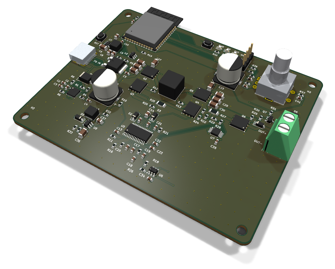
Pd brick is an open-source printed circuit board by enkhbold470, from the enkhbold470/pd-brick repository on GitHub, published under the CERN-OHL-S-2.0 licence. It is a 4-layer board of 100 × 80 mm with 120 parts on 104 nets, routed with 908 tracks and 208 vias.
It is built around the ESP32-S3-WROOM-1-N8R8, LM5176PWPR and MT3608, with the USBLC6-2SC6, CL31A106KBHNNNE and CC0603KRX7R9BB104 among its other parts. Its parts include 42 resistors, 41 capacitors, 9 diodes, 8 ICs and 7 transistors. It belongs with the power boards and the ESP32 boards of this library.


A USB-C Power Delivery bench supply: STUSB4500 sink, LM5176 buck-boost, 1.2-22 V set over I2C by an ESP32-S3.
Part of the KiCad projects portfolio. Gerbers are in fab/gerbers/ and zipped in fab/.
| Layers | Size | Parts | Nets | Connections routed | Vias | ERC errors | DRC errors / unconnected / parity |
|---|---|---|---|---|---|---|---|
| 4 | 100 x 80 mm | 120 | 71 | 283 -> 0 open | 208 | 0 | 0 / 0 / 0 |
Not fabricated, assembled or powered. Every number on this page is measured by KiCad 10 on the files in this folder; the full measurements are in report.json.
| KiCad project | kicad/ |
| Gerbers, BOM, CPL, STEP, schematic PDF | fab/ |
| Renders | top, bottom |
| Design process, every step as KiCad rendered it | media/design-process.mp4 |
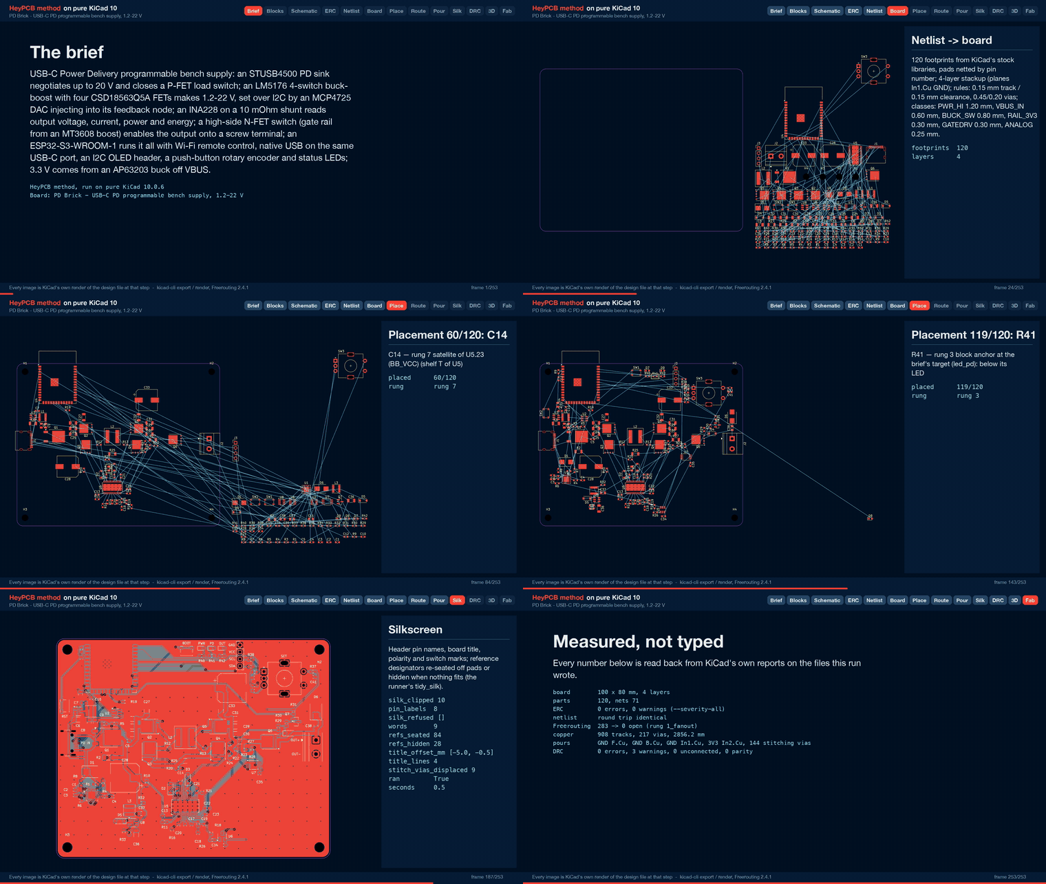
PD Brick is a USB-C Power Delivery programmable bench supply with a 1.2-22 V output. It was designed with the HeyPCB method on KiCad 10. A headless pipeline (KiCad 10.0.6, Freerouting 2.4.1) took the brief in board.json through schematic, placement, routing, pours, DRC and fab outputs.
This board has not been fabricated, assembled or powered. There is no firmware. On the final run it passes these checks:
The fab gate is ready. Everything under "Check before ordering" is a datasheet calculation or a layout measurement, not a bench result.
Input: USB-C, USB PD 3.0 sink up to 20 V (ST STUSB4500). The controller closes an AOD4185 P-FET between the receptacle and the power stage. There is a 24 V TVS on the receptacle.
Converter: TI LM5176 4-switch buck-boost at about 390 kHz, with:
The output is about 1.2-22 V.
Setpoint: a Microchip MCP4725 12-bit I2C DAC injects into the LM5176 feedback node through 15k. A higher code gives a lower voltage.
Monitor: a TI INA228 (20-bit V / I / power / energy) on a 10 mOhm high-side output shunt. It shares the LM5176's average-current-limit filter on the same shunt (50 mV, about 5 A).
Output enable: one CSD18563Q5A high-side N-FET. Its gate is pulled up from a 25.6 V rail made by an MT3608 boost, Vgs is clamped at 12 V, and a 2N7002 pulls the gate down. The output is off from reset.
Output: Phoenix MKDS 1,5/2-5,08 screw terminal (17.5 A), with an SMBJ24A TVS and 1 uF across it.
MCU: ESP32-S3-WROOM-1-N8R8, from the HeyPCB block esp32_s3_minimal:
3.3 V: Diodes AP63203 buck from VBUS (3.8-32 V in). An LDO would burn up to 8 W from a 20 V contract.
UI:
Board: 100 x 80 mm, four M3 holes, 4 layers:
| Asked for | Fitted | Why |
|---|---|---|
| TPS55289 (or similar) I2C buck-boost | LM5176 controller + 4 x CSD18563Q5A + MCP4725 DAC | KiCad 10 has no TPS55289 (or TPS552xx) symbol, and the live JLC lookup returned no TPS55289 row. The LM5176 (Regulator_Switching:LM5176PWP, LCSC C442493) has no I2C, so the DAC programs its FB node. |
| STUSB4500, AP33772 or CH224K | STUSB4500 | All three have KiCad 10 symbols. The AP33772 returned no JLC row. The CH224K is pin-strapped, with no I2C. The STUSB4500 (C2678061) renegotiates over I2C at 0x28. |
| INA228 (or INA226) | INA228 | Sensor_Energy:INA228, C2887910. |
| Load switch or MOSFET | one CSD18563Q5A high-side N-FET + MT3608 gate rail | No KiCad 10 load switch covers 1-22 V at several amps. A P-FET cannot turn on at a 1 V output. A low-side switch is bypassed by any second ground (a scope, or a USB-powered load). |
| (VBUS switch for VBUS_EN_SNK) | AOD4185 on the generic Transistor_FET:Q_PMOS_GDS symbol | KiCad 10 has no AOD4185 symbol. Q_PMOS_GDS (1 G, 2 D, 3 S) is this part's TO-252 land (tab = drain). |
| (power FETs) | CSD18563Q5A, 5 x 6 mm | The 3.3 x 3.3 mm CSD18543Q3A was tried first. Its KiCad VSON land puts the gate pad 0.14 mm from a source pad, so DRC fails at 0.2 mm on the footprint itself. |
USB-C -VBUS-> AOD4185 (STUSB4500 VBUS_EN_SNK) -VIN-> LM5176 buck-boost -VOUT-> 10 mOhm shunt -VOUT_SH-> N-FET -OUT_P-> terminal
   |                                                ^ FB <- 15k <- MCP4725 (I2C)   |  ISNS 100R/100R/1uF -> LM5176 + INA228
   +-VBUS-> AP63203 -3V3-> ESP32-S3, STUSB4500 I2C side, INA228, DAC, OLED, encoder          gate <- 1M <- 25.6 V (MT3608 off VIN)
Setting the output. FB has 100k from VOUT and 4.7k to GND, and the DAC drives FB through 15k:
VOUT = 0.8 V x (1 + 100/4.7 + 100/15) - VDAC x 100/15
That is about 23.2 V at code 0 and 1.2 V at full scale. Firmware clamps the code to 1.2-22 V.
Order at power-up.
Wide power nets. No 1.2 mm power track lands on an IC pin. On the routed board, the seven power-path nets reach only FETs, the inductor, passives, the TVS, the zener and the terminal. Every IC pin on a power net hangs off it through a resistor, placed at the power node (an at target in the brief):
I2C (IO38 SDA, IO39 SCL, 4.7k pull-ups):
ESP32-S3 pins. All GPIOs are on the module's right column and bottom row, which face the board:
| Pin | Function |
|---|---|
| IO42 / IO41 / IO40 | encoder A / B / switch |
| IO1 / IO2 | PD / OUT LEDs |
| IO10 | PD_RST |
| IO11 | PD_ALERT |
| IO12 | BB_EN |
| IO14 | OUT_OFF |
| IO19 / IO20 | USB D- / D+ |
| IO0 | BOOT |
The LM5176 PGOOD, the INA228 ALERT and a VIN divider were cut to shorten routing; the INA228 and STUSB4500 report the same information over I2C.
Gate numbers come from report.json. Rows marked "on the board" were measured on kicad/pd_brick.kicad_pcb with KiCad's Python (pcbnew, read-only scripts). Current ratings use ipc2221_amps from the pipeline (IPC-2221, 1 oz outer, 0.5 oz inner). A path's rating is the total current at which its busiest segment reaches its own rating at a 20 C rise. The share each segment carries comes from solving the net's copper as a resistor network, with the source pads tied (ideal contacts).
| Gate | Result |
|---|---|
| Composition | 18 block instances, 16 distinct blocks (11 written for this board, 5 reused) → 120 footprints, 71 nets |
| Part binding | 116 of 116 BOM parts bound to a pinned LCSC table, 0 unsourced, 0 conflicts. H1-H4 are drilled M3 holes, kept out of the BOM. 23 distinct Extended parts, about $69 in JLC loading fees. 1 warning: the 10k 0603 R9 (C25804, the ESP32 EN pull-up) had 0 stock at its 2026-06-23 snapshot |
ERC (kicad-cli sch erc --severity-all) | 0 errors, 0 warnings |
| Netlist round trip | identical, 71 nets |
| Freerouting, rung 1, fanout on (kept) | 283 → 0 open in 160.9 s, with no last-mile help. DRC score 0, 73 vias |
| Freerouting, rung 1, fanout off (for comparison) | 283 → 1 open (VOUT, R17.1 to C29.1) in 38.4 s. The last-mile router found no path, so this rung was not kept |
| Copper | 908 tracks, 73 routing vias, 2856.2 mm of track (F.Cu 1624.4, In2 1030.5, B.Cu 201.3). No segment was widened, kept narrow or raised: every segment is at its class width (also checked on the board) |
| VBUS input (on the board) | 0.6 mm, all on F.Cu, no vias. Each receptacle VBUS pad pair has its own track to Q1's source pad: 8.6 mm from A4/B9 and 7.5 mm from A9/B4. No segment is shared; the two tracks meet only inside the source pad. They split the current 45 / 55. Path rating 4.07 A at a 20 C rise (3.0 A at 10 C) |
| Power path (on the board) | VIN, BB_SW1, BB_SW2, BB_CS, VOUT, VOUT_SH and OUT_P run only on F.Cu at 1.2 mm, with no vias and no necks. OUT_P's branch to the output TVS is F.Cu too. VIN from Q1 to the buck high-side FET, and the output path (VOUT, VOUT_SH, OUT_P) to the terminal, each rate 3.70 A at a 20 C rise |
| 3.3 V buck (on the board) | Switch node 0.8 mm on F.Cu, no vias: 1.6 mm from the AP63203's SW pin to the inductor pad, 5.1 mm with the branch to the bootstrap cap. Rated 2.76 A at a 20 C rise. 3V3 is 0.3 mm everywhere (271.5 mm: F.Cu 87.9, In2 169.1, B.Cu 14.5, 10 vias), with the In2 3V3 pour around it |
| Pours (only after a measured 0 open) | GND on F.Cu, B.Cu and In1; 3V3 on In2. 144 stitching vias, 0 island-repair vias, still 0 open. 217 vias in all |
DRC (kicad-cli pcb drc --severity-all --schematic-parity) | fresh: 0 errors, 3 warnings, 0 unconnected, 0 parity |
DFM (jlcpcb_4layer) | 0 errors, 1 warning: 338 stock-footprint silk strokes at 0.12 mm, which the fab prints at its 0.15 mm minimum |
| Fab gate | ready, no blockers. Outputs: gerbers for four copper layers (the gerber job says 4 layers, 1.6 mm), drill, BOM, JLC placement file (8 rotations corrected), position file, schematic PDF, STEP |
lib_footprint_mismatch on three parts: the USB-C receptacle (J1), the terminal (J2) and the ESP32-S3 module (U4).
report.json, texts read back on the board).
media/design-process.mp4) is 168.6 s long (ffprobe on the run's own MP4), made from 253 stills. It ends on the fab card.--no-media, then the full run with media) routed identically: 908 tracks, 73 vias, 2856.2 mm, and the same VBUS feeds and split. A brief change is a new sample, though. Adding one more F.Cu keep-out (under the receptacle body) routed the VBUS feeds into one shared 0.6 mm track again (see below). After the final run, only why texts in board.json were corrected; nothing they feed changed.The schematic packer. It could not fit one 52-part buck-boost block on A1 (993 mm wide), so the block was split into a controller block and a power-stage block.
Sense resistors at the power nodes. Left to the shelf placer, they landed under the controller. Every 1.5 mm power track then had to cross the controller's satellites, and Freerouting stalled at 22 unrouted.
The output switch. A back-to-back (source-to-source) pair was tried first. With the S-S-S-G pinout, one gate always sits across the wide source-to-source track, and that gate net was left open in four of six rebuilds. The board now uses a single FET (see "Check before ordering").
An early 0-open route ran the output (OUT_P) through one via and 17.9 mm of In2: about 1.3 A on 0.5 oz inner copper. Placing the terminal pin level with the FET drain moved it to F.Cu. On the final board, OUT_P has no inner-layer copper at all.
The VBUS input. On the previous build, the last 7.8 mm of VBUS into Q1 was a single 0.6 mm track carrying all the input current. That is 2.24 A at a 20 C rise, and about a 39 C rise at 3 A. Freerouting had left the A9/B4 pad pair unrouted because its CC2 fan-out via sat too close to that pad's exit. The last-mile router then joined that pair onto the other pair's track. A wider class cannot help: the receptacle's VBUS pads are 0.6 mm wide, 0.2 mm from the GND pad beside them, and Freerouting runs with neckdown off. What fixed it, over four --no-media runs:
J1-B9 -> J1-A9 unrouted.board.keepouts add:
The 3.3 V buck. Before, the switch node was a 0.15 mm track (about 0.8 A), and the output caps sat on the far side of the IC from the inductor. Now the IC, inductor and four caps are locked as one cell:
The switch node has its own 0.8 mm class and 3V3 a 0.3 mm class.
Silk. On the previous build, 4 of 7 words fit (BOOT, RST and the OUT LED's word did not), the terminal had no + / - mark, and 0 of 8 OLED pin labels fit. The fixes were all in the brief:
silk.switches entry. silk.polarity tries spots 1.9-2.3 mm from each pin, and every one of them hits the terminal's own 2.6 mm pads or its body outline.Rules.
All are inside the DFM profile.
Gate-drive and feedback lengths. The controller sits below the power stage. Measured on the board, pin to pin:
Both work against switching performance and noise. A hand-tuned layout would put the controller beside the FETs.
Output TVS. D6 reaches the terminal pin through 10.0 mm of F.Cu, with no via. A TVS clamps best right at the terminal. The 1 uF (C38) is 4.2 mm away on F.Cu.
VBUS under the receptacle. The 3.3 V buck's VBUS feed runs on F.Cu under the USB-C receptacle's body (a straight 11.4 mm along x = 4.67 mm), with only solder mask between it and the receptacle's GND shell. It carries only the buck's input current. A brief keep-out there was tried, and it merged the two main VBUS feeds into one shared 0.6 mm track again (2.24 A), so it was dropped. Check the receptacle's seating, or move that feed by hand, before ordering.
Compensation (33k + 10 nF, 100 pF across) is a first-pass calculation for about 4-5 kHz crossover with the 220 uF output bulk. Check the loop on the bench with load steps at 5, 9, 15 and 20 V inputs.
Low outputs from high inputs. 1.2 V out from 20 V in is a 6 % duty cycle, about 150 ns on-time at 390 kHz. The LM5176 datasheet gives no minimum on-time. Firmware should renegotiate the lowest PDO that covers the setpoint.
VISNS is taken from the LM5176's filtered VIN-pin node (10 ohm + 100 nF), not from VIN itself. The 10 ohm drop at the VIN-pin current (tens of mV) offsets the buck/boost mode-transition sense slightly.
Power-up state of the DAC. The MCP4725 powers up at its EEPROM code (factory mid-scale, about 12 V). Write the lowest-output code to EEPROM on first boot, and enable the converter only after writing the DAC.
VBUS switch at attach. With default NVM, the STUSB4500 closes the P-FET at a 5 V attach, before any PD contract, into about 260 uF of input capacitance. A 100 ohm + 100 nF gate-drain network slows the turn-on; the inrush has not been measured.
OLED pin order. The header is GND, VCC, SCL, SDA, and the silk now prints those names beside the pins. Some 1.3" modules swap GND and VCC, so match the module to the silk.
Encoder variant. EC11E15244G1 was picked for the EC11E-Switch footprint from a live lookup. Confirm it has the push switch and the detent count you want.
Ground is shared. OUT- is board GND, which is the USB source's ground. The output is not isolated.
USB D+/D-. Both are 0.15 mm tracks with no necks.
Part numbers.
board.json is the brief. It holds the blocks, the nets, the placement, the keep-outs, the silk and these net classes:
report.json is the run's report. Every gate number above comes from it.kicad/ is the KiCad 10 project (pd_brick.kicad_pro, pd_brick.kicad_sch, pd_brick.kicad_pcb) with its 3D models/.fab/ holds the fab outputs:
pd_brick_gerbers.zip: four copper layers, mask, paste, silk, outline, drill and the gerber job file;pd_brick_bom.csv: 57 lines, 116 parts, each with an LCSC number;pd_brick_cpl_jlc.csv: 113 SMD placements for JLCPCB. J2, J3 and SW3 are through-hole and appear only in the BOM;pd_brick_pos.csv: KiCad's position file;pd_brick_schematic.pdf;pd_brick.step.media/ holds the renders (hero.png, top.png, bottom.png) and the design-process video (design-process.mp4, design-process.gif).| Qty | Value | Footprint | References |
|---|---|---|---|
| 9 | 10uF | Capacitor_SMD:C_1206_3216Metric | C6, C24, C25, C26, C27, C29, C30, C31, C32 |
| 8 | 100nF | Capacitor_SMD:C_0603_1608Metric | C5, C7, C10, C13, C15, C16, C34, C35 |
| 8 | 4.7k | Resistor_SMD:R_0603_1608Metric | R7, R18, R30, R35, R36, R37, R38, R39 |
| 6 | 1uF | Capacitor_SMD:C_0603_1608Metric | C1, C2, C3, C4, C12, C22 |
| 5 | 10 | Resistor_SMD:R_0603_1608Metric | R8, R10, R24, R28, R32 |
| 5 | 100 | Resistor_SMD:R_0603_1608Metric | R5, R20, R21, R22, R23 |
| 5 | CSD18563Q5A | Package_TO_SOT_SMD:TDSON-8-1 | Q2, Q3, Q4, Q5, Q6 |
| 4 | 100k | Resistor_SMD:R_0603_1608Metric | R3, R6, R17, R19 |
| 4 | 10nF | Capacitor_SMD:C_0603_1608Metric | C18, C39, C40, C41 |
| 4 | M3 | MountingHole:MountingHole_3.2mm_M3 | H1, H2, H3, H4 |
| 3 | 1k | Resistor_SMD:R_0603_1608Metric | R1, R41, R42 |
| 3 | 22uF | Capacitor_SMD:C_0805_2012Metric | C8, C9, C11 |
| 3 | B5819W | Diode_SMD:D_SOD-123 | D2, D3, D5 |
| 2 | 1 | Resistor_SMD:R_0603_1608Metric | R12, R13 |
| 2 | 100pF | Capacitor_SMD:C_0603_1608Metric | C19, C23 |
| 2 | 10m | Resistor_SMD:R_1206_3216Metric | R25, R27 |
| 2 | 1M | Resistor_SMD:R_0603_1608Metric | R29, R33 |
| 2 | 1uF | Capacitor_SMD:C_0805_2012Metric | C37, C38 |
| 2 | 220uF 50V | Capacitor_SMD:CP_Elec_10x10 | C28, C33 |
| 2 | 22k | Resistor_SMD:R_0603_1608Metric | R4, R31 |
| 2 | SMBJ24A | Diode_SMD:D_SMB | D1, D6 |
| 1 | 10k | Resistor_SMD:R_0603_1608Metric | R9 |
| 1 | 15k | Resistor_SMD:R_0603_1608Metric | R26 |
| 1 | 1k | Resistor_SMD:R_1206_3216Metric | R2 |
| 1 | 2.2k | Resistor_SMD:R_0603_1608Metric | R40 |
| 1 | 20k | Resistor_SMD:R_0603_1608Metric | R14 |
| 1 | 220pF | Capacitor_SMD:C_0603_1608Metric | C20 |
| 1 | 22uH | Inductor_SMD:L_Changjiang_FNR4030S | L3 |
| 1 | 24k | Resistor_SMD:R_0603_1608Metric | R34 |
| 1 | 2N7002 | Package_TO_SOT_SMD:SOT-23 | Q7 |
| 1 | 2k | Resistor_SMD:R_0603_1608Metric | R11 |
| 1 | 33k | Resistor_SMD:R_0603_1608Metric | R15 |
| 1 | 33nF | Capacitor_SMD:C_0603_1608Metric | C17 |
| 1 | 4.7uF | Capacitor_SMD:C_0805_2012Metric | C14 |
| 1 | 4.7uF | Capacitor_SMD:C_1206_3216Metric | C36 |
| 1 | 4.7uH | Inductor_SMD:L_Sunlord_SWPA4030S | L1 |
| 1 | 4.7uH | Inductor_SMD:L_Coilcraft_XAL7070-XXX | L2 |
| 1 | 47pF | Capacitor_SMD:C_0603_1608Metric | C21 |
| 1 | 82k | Resistor_SMD:R_0603_1608Metric | R16 |
| 1 | AOD4185 | Package_TO_SOT_SMD:TO-252-2 | Q1 |
| 1 | AP63203WU-7 | Package_TO_SOT_SMD:TSOT-23-6 | U3 |
| 1 | BOOT | Button_Switch_SMD:SW_SPST_PTS810 | SW1 |
| 1 | BZT52C12 | Diode_SMD:D_SOD-123 | D4 |
| 1 | EC11E15244G1 | Rotary_Encoder:RotaryEncoder_Alps_EC11E-Switch_Vertical_H20mm | SW3 |
| 1 | ESP32-S3-WROOM-1-N8R8 | RF_Module:ESP32-S3-WROOM-1 | U4 |
| 1 | Green (PD) | LED_SMD:LED_0603_1608Metric | D8 |
| 1 | Green (PWR) | LED_SMD:LED_0603_1608Metric | D7 |
| 1 | INA228AIDGSR | Package_SO:TSSOP-10_3x3mm_P0.5mm | U7 |
| 1 | LM5176PWPR | Package_SO:HTSSOP-28-1EP_4.4x9.7mm_P0.65mm_EP3.4x9.5mm_ThermalVias | U5 |
| 1 | MCP4725A0T-E/CH | Package_TO_SOT_SMD:SOT-23-6 | U6 |
| 1 | MT3608 | Package_TO_SOT_SMD:SOT-23-6 | U8 |
| 1 | OLED | Connector_PinHeader_2.54mm:PinHeader_1x04_P2.54mm_Vertical | J3 |
| 1 | OUT | TerminalBlock_Phoenix:TerminalBlock_Phoenix_MKDS-1,5-2-5.08_1x02_P5.08mm_Horizontal | J2 |
| 1 | RESET | Button_Switch_SMD:SW_SPST_PTS810 | SW2 |
| 1 | Red (OUT) | LED_SMD:LED_0603_1608Metric | D9 |
| 1 | STUSB4500QTR | Package_DFN_QFN:QFN-24-1EP_4x4mm_P0.5mm_EP2.7x2.7mm | U1 |
| 1 | USB-C PD | Connector_USB:USB_C_Receptacle_HRO_TYPE-C-31-M-12 | J1 |
| 1 | USBLC6-2SC6 | Package_TO_SOT_SMD:SOT-23-6 | U2 |
It measures 100 × 80 mm and has 4 copper layers, 1.6 mm thick.
120 parts, built around the ESP32-S3-WROOM-1-N8R8, LM5176PWPR, MT3608 and USBLC6-2SC6. The full list of its parts is on this page, with links to each part's symbol and footprint where PCBKit's library has them.
From the enkhbold470/pd-brick repository on GitHub, at the commit this page was made from: the board is kicad/pd_brick.kicad_pcb and its schematic kicad/pd_brick.kicad_sch. PCBKit opens the board in the browser, with nothing to install.
Its repository publishes it under the CERN-OHL-S-2.0 licence: you may reuse it on that licence's terms (keep the author's notice, and for a copyleft licence share your changes alike).
HeyPCB/power-kit
Six open power and charging boards: KiCad 10, JLCPCB-ready, CERN-OHL-S-2.0

vyrubaev/TV-Lift-Controller
TVLift Controller is an intelligent controller for TV lift and lower mechanisms, based on the ESP32 microcontroller.

osy/XG_Mobile_Station
Open source eGPU dock for ROG Ally and ROG Flow

udaravima/Lab_Bench
A modular, rack-style DC power supply: up to 8 hot-pluggable 600 W buck modules on a shared DC input bus, coordinated by a central manager over CAN.


CGainsWorks/emb-drone-flight-stack
Open-source quadrotor flight stack: custom KiCad flight-controller and power distribution boards plus C++ firmware with a PID attitude loop, written from scratch.

chinawrj/FarmMesh-Node
Developing an integrated hardware and software solution for farm-wide Mesh networking: RP2350B/ESP32-C5 nodes, firmware, network protocols, and Wi-Fi/BLE sensor access.

Diode663/ESP32_4-20mA_Sensor
Single-channel industrial 4-20 mA current-loop reader for ESPHome / Home Assistant. ESP32-S3 + INA226, USB-C powered, 24 V loop supply with a constant-current limiter. KiCad 10, generated from Python.