2 layers30 × 20 mm
Smoke
catuta0/fruta-midi-controller
Controlador MIDI USB de fruta (estilo Playtron) com Raspberry Pi Pico + MPR121 — Windows e Mac
2 partsMIT

 catuta0/fruta-midi-controller
Controlador MIDI USB de fruta (estilo Playtron) com Raspberry Pi Pico + MPR121 — Windows e Mac
Frutamidi is an open-source printed circuit board by catuta0, from the catuta0/fruta-midi-controller repository on GitHub, published under the MIT licence. It is a 2-layer board of 100 × 70 mm with 28 parts on 67 nets, routed with 91 tracks and 0 vias.
It is built around the SC0915, MFR-12FTF52-3K3 and MFR-12FTF52-220R, with the MFR-12FTF52-4K7 and B3F-1000 among its other parts. Its parts include 16 resistors, 3 connectors and 1 switch. It belongs with the audio and music boards and the RP2040 boards of this library.


A 100 × 70 mm board with copper on the bottom side only, designed for chemical etching at home (toner transfer or photosensitive board). It takes a Raspberry Pi Pico and an Adafruit MPR121 module (1982), both socketed, plus 14 screw terminals, a button, a potentiometer, a 3.3 kΩ series resistor on each electrode, two I²C pull-up resistors and two 220 Ω I²C series resistors.
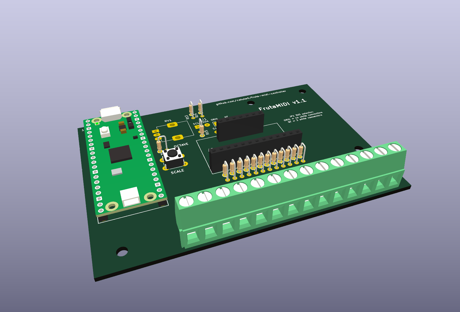
Status: the schematic passes ERC and the PCB passes DRC, both with no violations, and the PCB matches the schematic. The board has not yet been fabricated or physically tested. If you make one, open an issue with the result.
| File | Purpose |
|---|---|
fabrication/1-copper-for-transfer.pdf | What you print for toner or positive photosensitive board. 1:1 scale, already in the right orientation |
fabrication/1b-copper-negative.pdf | The same in negative, only for dry film / negative resist |
fabrication/2-assembly-map.pdf | Where each component goes, seen from the top |
fabrication/3-silkscreen-optional-mirrored.pdf | Optional: transfer the labels onto the component side |
fabrication/frutamidi-schematic.pdf | Schematic |
fabrication/gerbers/ | Gerbers + Excellon drill files, if you prefer to order the board (JLCPCB, PCBWay…) |
fabrication/bom-kicad.csv | BOM exported from KiCad, with manufacturer and part number columns |
frutamidi.kicad_pro / .kicad_sch / .kicad_pcb | KiCad 10 project, with its own libraries (FrutaMIDI.kicad_sym, FrutaMIDI.pretty/) |
scripts/ | Schematic and PCB generators, and build_all.sh (regenerates, checks and exports) |
| Ref. | Part | Qty | Approx. price | Notes |
|---|---|---|---|---|
| A1 | Raspberry Pi Pico, Raspberry Pi SC0915 (or Pico H, Pico W, Pico 2, Pico 2 W) | 1 | 5–8 € | The SC0915 has no headers: solder 2 × 1×20 male 2.54 mm headers to it. The "H" version comes with them fitted |
| — | Male header 1×20, 2.54 mm pitch | 2 | — | For the SC0915 only |
| A2 | Adafruit MPR121 12-key capacitive touch breakout, Adafruit 1982 | 1 | 9–12 € | Original or STEMMA QT: both work (see section 5). Comes with the male header to solder onto the module |
| R1–R12 | Resistor 3.3 kΩ (3k3), axial, DIN0204 size, Yageo MFR-12FTF52-3K3 | 12 | — | One in series with each electrode; mounted vertically |
| R13, R14 | Resistor 4.7 kΩ (4k7), axial, DIN0204 size, Yageo MFR-12FTF52-4K7 | 2 | — | I²C pull-ups (SCL, SDA); mounted vertically |
| R15, R16 | Resistor 220 Ω, axial, DIN0204 size, Yageo MFR-12FTF52-220R | 2 | — | In series in SCL (R15) and SDA (R16) on the Pico side; they limit the current if a configuration wire goes to the wrong hole; mounted vertically |
| A1 socket | Female header 1×20, 2.54 mm pitch (generic) | 2 | 1 € | Pico socket |
| A2 socket | Female header 1×13, 2.54 mm pitch (generic) | 1 | 0.50 € | Module electrode row |
| A2 socket | Female header 1×7, 2.54 mm pitch (generic) | 1 | 0.40 € | Module power/I²C row |
| J2 | 2-way screw terminal block, 5.08 mm pitch, interlocking, Phoenix Contact 1715721 (MKDS 1,5/ 2-5,08) or equivalent | 7 | 2–3 € | They lock together to form the 14-way strip |
| SW1 | 6 × 6 mm push button, 4 legs, Omron B3F-1000 | 1 | 0.20 € | Choose the height to suit the enclosure |
| RV1 | 10 kΩ linear potentiometer (B10K), 9 mm, vertical, Alps Alpine RK09K series | 1 | 1 € | Plus a knob |
| JP1 | Solder bridge (no part) | — | — | Bridged with solder or a resistor lead off-cut; see section 5 |
| — | Thin insulated solid wire (from network cable, for example) | ~10 cm | — | 2 configuration wires (SDA, SCL) |
| H1–H4 | M3 screws + spacers | 4 | 2 € | Optional |
| — | Micro-USB data cable | 1 | 3 € |
If you cut 40-way female header to length, you lose one pin at each cut: 2 strips of 1×40 are enough: one for 20 + 13, the other for 20 + 7.
| Part | Qty | Notes |
|---|---|---|
| Single-sided copper board, FR4 or FR2, 100 × 70 mm (35 µm) | 1 | Or cut from a larger one |
| Toner: laser printer + transfer paper (or glossy magazine paper) + clothes iron | — | Inkjet ink does not work |
| Photographic: positive pre-sensitised board + transparency film + UV lamp + developer (sodium hydroxide) | — | Alternative to toner |
| Ferric chloride (or sodium persulfate) | ~0.5 L | See the safety note in section 2 |
| Plastic container, nitrile gloves, goggles | — | Nothing metal |
| Acetone or thinner, fine steel wool, isopropyl alcohol | — | Cleaning |
| Fine permanent marker | 1 | Touching up toner gaps |
| Drill bits of 0.8 · 0.9 · 1.0 · 1.1 · 1.4 · 1.8 · 3.2 mm, plus a round needle file | 1 each | Mini drill, preferably on a stand |
| Soldering iron, flux-core solder (0.8 mm), multimeter | — |
| Rule | Value |
|---|---|
| Copper layers | Bottom only; all components through-hole on top |
| Track width | 1.0 mm (signals) and 1.2 mm (GND, 3V3); 0.8 mm on the short connections of the S row |
| Minimum clearance | 0.6 mm (project rule); 0.5 mm is the absolute minimum accepted by DRC |
| Pads | Minimum annular ring 0.40 mm. Pico socket 2.4 × 1.8 mm, module headers 1.8 × 2.4 mm (0.74 mm between pads on the 2.54 mm pitch), potentiometer 2.6 × 1.8 mm (0.70 mm between pads), 3.0 mm on the terminals |
| Vias and bridges | No vias. Only the JP1 solder bridge and the 2 module configuration wires |
| Ground plane | None, on purpose: copper around the electrode tracks takes away sensitivity |
1-copper-for-transfer.pdf and print at actual size / 100 %, without "fit to page".The small dots in the centre of the pads are left without copper after etching and act as a guide for the drill.
Preparing the board: cut it to 100 × 70 mm and rub the copper with steel wool until it shines. Clean it with alcohol and do not touch it with your fingers again.
Toner
Positive photosensitive
Etching
Safety: wear gloves and goggles, in a ventilated place. Ferric chloride stains everything permanently and is corrosive. Do not pour the used solution down the drain: it contains dissolved copper, so take it to a recycling/waste collection centre. If you use hydrochloric acid with hydrogen peroxide, always mix it in small quantities and outdoors, because it releases toxic gases.
Drill from the copper side, using the dots as a guide. There are 131 holes in total: 129 round holes and the 2 potentiometer slots.
| Bit | Holes | Where |
|---|---|---|
| 0.8 mm | 35 | Resistors R1–R16 (32) and JP1 (3) |
| 0.9 mm | 9 | J3, the S1–S7 wire holes (7), and J1 (2, configuration wires) |
| 1.0 mm | 63 | Female headers for the Pico (40) and the module (20), potentiometer pins (3) |
| 1.1 mm | 4 | Button |
| 1.4 mm | 14 | Screw terminals |
| 1.8 mm, then widen | 2 | Potentiometer mounting tabs (slots of 2.1 × 1.8 mm in the design; see below) |
| 3.2 mm | 4 | M3 mounting (optional; not plated) |
Potentiometer tab slots. Drill the two potentiometer tab holes with a 1.8 mm bit, then widen each one along the long side of its pad (left-right, the 4 mm direction) to about 2.1 mm with a round needle file or by rocking the 1.8 mm bit sideways. Test-fit the pot before soldering; the tabs must drop in without force.
If you like, apply flux or protective lacquer to the copper after drilling. You can also tin the tracks with the iron so they do not oxidise.
Solder from the lowest component to the tallest, so the board sits flat on the table. Use the assembly map.
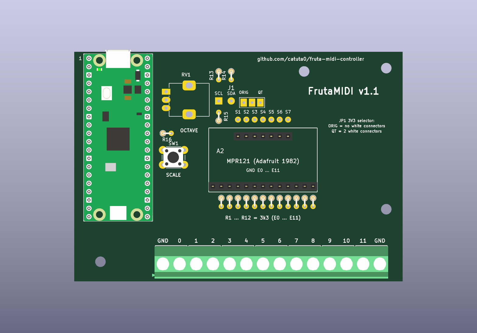
The Adafruit 1982 exists in two versions, with the 7 power/I²C pins in a different order. That is why the board does not connect them directly. Above the 7 module pins there are 7 holes S1–S7 (J3), each one directly above a module pin. You configure the board for your module in two steps.
Step 1: power (JP1). JP1 is a 3-pad solder bridge. The centre pad is 3V3. Bridge it to one side with solder or a resistor lead off-cut:
The silkscreen legend to the right of the module repeats this: "JP1 3V3 selector: / ORIG = no white connectors / QT = 2 white connectors".
Step 2: I²C (two wires). J1 has 2 holes, SCL on the left and SDA on the right. Connect:
To confirm, read the letters printed on the module next to the 7-pin row, and check this table:
| Version | How to recognise it | JP1 | SDA → | SCL → |
|---|---|---|---|---|
| Original | No small white connectors | ORIG | S5 | S6 |
| STEMMA QT (current) | Two small white 4-pin connectors (STEMMA QT / Qwiic) | QT | S3 | S4 |
Use insulated solid wire and run it on the component side. Solder the two wires underneath, on the copper. The other S holes stay empty. The module's GND needs no wire: it comes in through the electrode row and is the same in both versions.
A wrong JP1 position can damage the sensor. ORIG on a STEMMA QT module puts 3V3 on the module's ADDR pin; QT on an original module puts it on IRQ. The MPR121 chip is then unpowered, so 3V3 on that pin is above its absolute maximum rating (VDD + 0.3 V), and it can back-feed the module through its 10 kΩ pull-ups. There is no direct short to GND, but the module is not supplied correctly, the sensor does not respond and the Pico LED blinks fast. Check JP1 against the table above before inserting the module (section 6). Never bridge all three pads.
With the multimeter, without the Pico or the module plugged in:
The board uses different pins from the breadboard, so it needs the PCB version of the firmware:
| Board | File (in Releases) |
|---|---|
| Raspberry Pi Pico | FrutaMIDI-pcb-rpipico.uf2 |
| Raspberry Pi Pico W | FrutaMIDI-pcb-rpipicow.uf2 |
| Raspberry Pi Pico 2 | FrutaMIDI-pcb-rpipico2.uf2 |
| Raspberry Pi Pico 2 W | FrutaMIDI-pcb-rpipico2w.uf2 |
.uf2 onto the RPI-RP2 drive (on the Pico 2: RP2350).If you compile it yourself, uncomment #define FRUTAMIDI_PCB at the start of FrutaMIDI.ino. This definition moves I²C to GP26/GP27 (Wire1), the button to GP22 and the potentiometer to GP28, and enables the potentiometer.
| Signal | Pico pin | GP |
|---|---|---|
| SDA (I²C1) | 31 | GP26 |
| SCL (I²C1) | 32 | GP27 |
| Button | 29 | GP22 |
| Potentiometer | 34 | GP28 / ADC2 |
| 3V3 | 36 | — |
| AGND | 33 | — |
| GND | 3, 8, 13, 18, 23, 28, 38 | — |
| Symptom | Likely cause | What to do |
|---|---|---|
| Pico LED blinks fast | Sensor not responding | Check that JP1 is bridged to the side for your version and that the 2 wires go to the right S holes; check that you uploaded the pcb .uf2 |
| Nothing happens when plugged in | Pico the wrong way round, or charge-only cable | USB towards the top edge; change the cable |
| One terminal is always playing | Copper or solder bridge between tracks | Look with a magnifier in the electrode fan-out and the resistor row; cut with a craft knife |
| Two terminals play together | Short between neighbouring tracks | Same procedure |
| One terminal never plays | Resistor of that electrode not soldered, or broken track | Measure about 3.3 kΩ from the terminal to the module header pin (section 6); resolder |
| The potentiometer does not change the octave | Breadboard firmware | Upload the pcb .uf2 |
| The octave jumps by itself | Potentiometer tab or pin badly soldered | Resolder RV1 |
Sensitivity problems (fruit, cables, ground) are the same as on the breadboard: see the design notes in the main README.
Each electrode has a 3.3 kΩ series resistor (R1–R12) between the screw terminal and the sensor. Its protection against IEC 61000-4-2 contact discharge at ±4 kV is an estimate that rests on assumptions (the sensor pin's surge limit is inferred, not specified), not a pass. The resistor is not rated for the pulse voltage across it. Only an ESD-gun test, ideally with a pulse-rated resistor, can confirm it. The board has not been evaluated for higher discharge levels or for touching while it is connected to mains-powered equipment. See the electronics analysis. Never connect the electrodes to anything plugged into mains power.
The schematic and the PCB are generated by the scripts in scripts/, not drawn by hand. To change something, edit gen_schematic.py / gen_pcb.py and run:
sh hardware/scripts/build_all.shThe script regenerates everything, runs ERC and DRC (it fails if there are violations), checks that the PCB matches the schematic and exports the fabrication/ folder again. The KiCad files also open and edit normally in KiCad 10, but if you edit them by hand, stop regenerating them with the script.
The module footprint was measured from Adafruit's Eagle files (CC BY-SA). Both versions have the same geometry: only the order of the 7-pin row changes.
| Qty | Value | Footprint | References |
|---|---|---|---|
| 12 | 3k3 | FrutaMIDI:R_Axial_DIN0204_P2.54mm_Vertical_HomeEtch | R1, R2, R3, R4, R5, R6, R7, R8, R9, R10, R11, R12 |
| 4 | M3 | FrutaMIDI:MountingHole_3.2mm_M3 | H1, H2, H3, H4 |
| 2 | 220 | FrutaMIDI:R_Axial_DIN0204_P2.54mm_Vertical_HomeEtch | R15, R16 |
| 2 | 4k7 | FrutaMIDI:R_Axial_DIN0204_P2.54mm_Vertical_HomeEtch | R13, R14 |
| 1 | 10k lin (B10K) | FrutaMIDI:Potentiometer_RK09K_Vertical | RV1 |
| 1 | 3V3_ORIG_QT | FrutaMIDI:SolderJumper_3_THT_P2.54mm | JP1 |
| 1 | Adafruit_MPR121_1982 | FrutaMIDI:Adafruit_MPR121_1982_Socket | A2 |
| 1 | CFG_SCL_SDA | FrutaMIDI:Config_2pads | J1 |
| 1 | RaspberryPi_Pico | FrutaMIDI:RaspberryPi_Pico_Socket | A1 |
| 1 | SW_Push_6mm | FrutaMIDI:SW_PUSH_6mm | SW1 |
| 1 | Screw terminals 5.08 mm (7x 2-way) | FrutaMIDI:TerminalBlock_5.08_1x14 | J2 |
| 1 | WIRE_HOLES_S1_S7 | FrutaMIDI:WireHoles_1x07_P2.54mm | J3 |
catuta0/fruta-midi-controller
Controlador MIDI USB de fruta (estilo Playtron) com Raspberry Pi Pico + MPR121 — Windows e Mac

Rack-Robotics/Powercore-V3
electrical-discharge power supply, open-source


jackw01/pi-pico-printer-board
Tinkerer-friendly Klipper compatible 3D printer control board using Raspberry Pi Pico


Supermagnum/Europe-ergo
A 94 key ergonomic, split keyboard suitable for European countries.

lambdaBoost/MC6205-graphical-display
graphical display on old neon plasma screen


It measures 100 × 70 mm and has 2 copper layers, 1.6 mm thick.
28 parts, built around the SC0915, MFR-12FTF52-3K3, MFR-12FTF52-220R and MFR-12FTF52-4K7. The full list of its parts is on this page, with links to each part's symbol and footprint where PCBKit's library has them.
From the catuta0/fruta-midi-controller repository on GitHub, at the commit this page was made from: the board is hardware/frutamidi.kicad_pcb and its schematic hardware/frutamidi.kicad_sch. PCBKit opens the board in the browser, with nothing to install.
Its repository publishes it under the MIT licence: you may reuse it on that licence's terms (keep the author's notice, and for a copyleft licence share your changes alike).