

4 layers58 × 66 mm
H616 devboard
Bogdan8266/h616-board
8-layer Allwinner H616/618 SBC with DDR3, USB, Wi-Fi/BT and battery power support, designed for embedded Linux.
165 parts4CERN-OHL-P-2.0

 Bogdan8266/h616-board4
8-layer Allwinner H616/618 SBC with DDR3, USB, Wi-Fi/BT and battery power support, designed for embedded Linux.
Debug Adapter is an open-source printed circuit board by Bogdan8266, from the Bogdan8266/h616-board repository on GitHub, published under the CERN-OHL-P-2.0 licence. It is a 2-layer board of 39.5 × 56 mm with 25 parts on 45 nets, routed with 251 tracks and 179 vias.
It is built around the SMAJ5.0A. Its parts include 9 capacitors, 6 resistors, 5 connectors, 2 diodes and 2 fuses. It belongs with the computers and single-board computers and power boards of this library.




A compact, battery-powered 64-bit ARM development board measuring 50 mm × 50 mm based on the Allwinner H616 Quad-Core Cortex-A53 SoC with integrated powerbank PMU, high-speed DDR3, eMMC 5.1, and dual-band Wi-Fi.
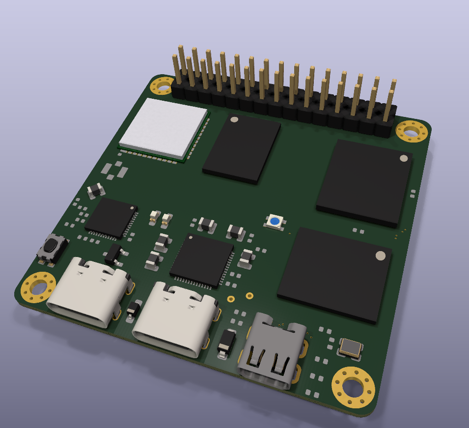
Unlike standard commercial H616 boards (Orange Pi, Banana Pi, etc.) that require a 5V/3A wall adapter and shut down the moment you unplug the cable, Nebula Board features an onboard bidirectional fast-charging system that runs from a single Li-ion cell (18650 / Li-Po) and recharges via USB-C with USB-PD / QC4+.
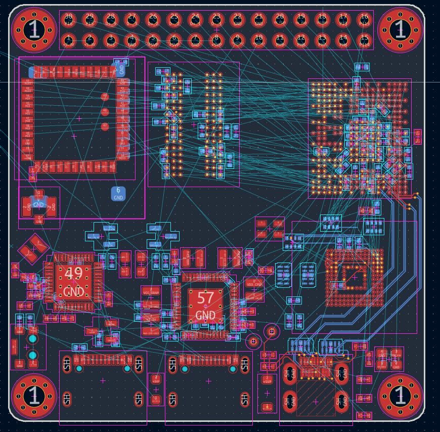
The PCB has been floorplanned to strictly separate high-speed digital buses, power conversion, and radio frequency:
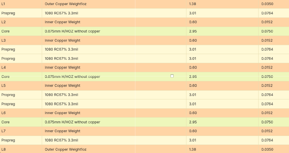
The board is designed around JLCPCB's standard 8-layer stackup JLC08101H-1080 with a finished thickness of 1.02 mm ±10%.
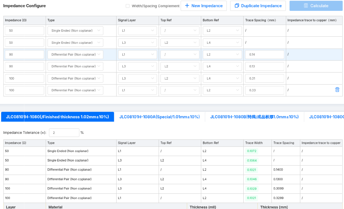
| Signal Group | Impedance | Layer | Trace Width | Spacing | Notes |
|---|---|---|---|---|---|
| RF / Single-Ended 50 Ω | $50\ \Omega$ | L1 (ref L2) | 0.107 mm | — | Wi-Fi 50 Ω line, eMMC, Clock |
| DDR3 Single-Ended 50 Ω | $50\ \Omega$ | L3 (ref L2/L4) | 0.106 mm | — | Inner stripline DDR3 DQ / Address |
| USB 2.0 Differential 90 Ω | $90\ \Omega$ | L1 (ref L2) | 0.102 mm | 0.140 mm | USB D+ / D- differential pairs |
| USB 2.0 Differential 90 Ω | $90\ \Omega$ | L3 (ref L2/L4) | 0.105 mm | 0.130 mm | Inner USB routing |
| HDMI / DDR Clock 100 Ω | $100\ \Omega$ | L1 (ref L2) | 0.102 mm | 0.330 mm | HDMI TMDS clock/data, DDR CK/DQS |
| HDMI / DDR Clock 100 Ω | $100\ \Omega$ | L3 (ref L2/L4) | 0.103 mm | 0.310 mm | Inner 100 Ω differential stripline |
[!IMPORTANT] To order this 8-layer board at promotional pricing without astronomical costs, keep minimum via hole size at 0.2 mm / 0.25 mm drill with a ≥0.4 mm pad (for a safe ≥0.1 mm annular ring). For BGA breakout, vias are placed via dog-bone or filled via-in-pad.
The board features a dual-PMIC architecture:
SW6206 (Battery & Fast Charger):
FLED/BSET 10k resistor).VOUTSP/VOUTSN) and synchronous buck-boost converter.+5VP_0) for the board whether running from an external wall charger or boosting from battery.0x3C) by H616.AXP305 (System PMIC):
+5VP_0 rail and steps it down via multiple high-efficiency DCDC buck converters:
Dual USB-C Topology:
D+/D-) with 5.1k CC pull-downs and Schottky diode power protection to +5VP_0. Allows flashing, ADB, Linux gadget networking, or USB host mode while on battery.The H616 supports 16-bit or 32-bit DRAM memory interfaces. According to the JEDEC standard, a single discrete DDR3 chip is 16-bit wide, so a single-chip design uses a 16-bit interface. Compatible 96-ball FBGA chips include:
H5TQ1G63BFR (1 Gb / 128 MB)H5TQ2G63BFR / H5TQ2G63DFR (2 Gb / 256 MB)H5TQ4G63AFR / H5TQ4G63CFR / H5TQ4G63MFR (4 Gb / 512 MB)H5TC8G63AMR / H5TC8G63CMR (8 Gb / 1 GB — DDR3L)K4B1G1646G / K4B1G1646I (1 Gb / 128 MB)K4B2G1646E / K4B2G1646F (2 Gb / 256 MB)K4B4G1646D / K4B4G1646E (4 Gb / 512 MB)K4B8G1646D / K4B8G1646B (8 Gb / 1 GB)MT41J64M16 (1 Gb / 128 MB)MT41J128M16 / MT41K128M16 (2 Gb / 256 MB)MT41J256M16 / MT41K256M16 (4 Gb / 512 MB)MT41J512M16 / MT41K512M16 (8 Gb / 1 GB)NT5CB64M16 (1 Gb / 128 MB)NT5CB128M16 / NT5CC128M16 (2 Gb / 256 MB)NT5CB256M16 / NT5CC256M16 (4 Gb / 512 MB)NT5CC512M16 (8 Gb / 1 GB)PG0–PG5).PG6–PG9).PG10 (X32KFOUT).U.FL_Hirose_U.FL-R-SMT-1_Vertical) right next to the module output with a 50 Ω coplanar waveguide and $\pi$-matching network. Connects to any standard 2.4/5GHz flexible FPC adhesive antenna.The board routes the H616 hardware Audio HUB I2S3 controller and I2C0 bus directly to the 40-pin header:
PH6 — H_I2S3_BCLK (Bit Clock)PH7 — H_I2S3_LRCK (Word Select / Left-Right Clock)PH8 — H_I2S3_DOUT0 (DAC Audio Output)PH9 — H_I2S3_DIN0 (ADC Audio Input)PI5 / PI6 — TWI0_SCK / TWI0_SDA (I2C0 bus)This allows building low-latency DSP daughterboards, such as a Neural Amp Modeler (NAM) guitar processor, Hi-Fi FLAC IEM DAC shield (PCM5102 / CS4272), or connecting micro-OLED status displays (SSD1306) via I2C. When audio drivers are disabled in the Device Tree, all pins function as standard 3.3V GPIOs.
For double-sided manual assembly with a hot plate and hot air rework station:
Mandatory Reading Before Soldering BGA by Hand

| Qty | Value | Footprint | References |
|---|---|---|---|
| 5 | 10u | Capacitor_SMD:C_0402_1005Metric_Pad0.74x0.62mm_HandSolder | C1, C2, C3, C4, C5 |
| 4 | 47u | Capacitor_SMD:C_1210_3225Metric_Pad1.33x2.70mm_HandSolder | C7, C8, C9, C10 |
| 4 | 5K1 | Resistor_SMD:R_0402_1005Metric | R2, R3, R4, R5 |
| 3 | USB_C_Receptacle_USB2.0_16P | Connector_USB:USB_C_Receptacle_GCT_USB4105-xx-A_16P_TopMnt_Horizontal | J2, J6, J7 |
| 2 | 22K | Resistor_SMD:R_0402_1005Metric | R6, R7 |
| 2 | Fuse_Small | Fuse:Fuse_1812_4532Metric_Pad1.30x3.40mm_HandSolder | F1, F2 |
| 2 | SMAJ5.0A | Diode_SMD:D_SMA | D1, D2 |
| 1 | Conn_01x08_MountingPin | Connector_FFC-FPC:TE_84952-8_1x08-1MP_P1.0mm_Horizontal | J3 |
| 1 | Conn_01x20_MountingPin | Connector_FFC-FPC:TE_2-84952-0_1x20-1MP_P1.0mm_Horizontal | J5 |
| 1 | GL823K | Package_SO:SSOP-16_3.9x4.9mm_P0.635mm | U1 |
Bogdan8266/h616-board
8-layer Allwinner H616/618 SBC with DDR3, USB, Wi-Fi/BT and battery power support, designed for embedded Linux.

Bogdan8266/h616-board
8-layer Allwinner H616/618 SBC with DDR3, USB, Wi-Fi/BT and battery power support, designed for embedded Linux.

Bogdan8266/h616-board
8-layer Allwinner H616/618 SBC with DDR3, USB, Wi-Fi/BT and battery power support, designed for embedded Linux.


brickbots/PiFinder
A plate solving telescope finder based around a Raspberry PI and RPI HQ Camera

tombueng/LuxDMX
Open-source Art-Net / sACN (E1.31) → DMX512 gateway for ESP32 / ESP32-S3 / Ethernet. Live web UI shows all 512 channels in real time, flags console conflicts, and drives galvanically-isolated DMX.


jackw01/pi-pico-printer-board
Tinkerer-friendly Klipper compatible 3D printer control board using Raspberry Pi Pico

bobberdolle1/SkySweep32
Open-source passive multi-band RF monitoring system | 855–925 MHz, 2.4 GHz, 5.8 GHz | Rev C first prototype

It measures 39.5 × 56 mm and has 2 copper layers, 1.6 mm thick.
25 parts, built around the SMAJ5.0A. The full list of its parts is on this page, with links to each part's symbol and footprint where PCBKit's library has them.
From the Bogdan8266/h616-board repository on GitHub, at the commit this page was made from: the board is Hardware/Debug_Adapter/Debug_Adapter.kicad_pcb and its schematic Hardware/Debug_Adapter/Debug_Adapter.kicad_sch. PCBKit opens the board in the browser, with nothing to install.
Its repository publishes it under the CERN-OHL-P-2.0 licence: you may reuse it on that licence's terms (keep the author's notice, and for a copyleft licence share your changes alike).