2 layers100 × 100 mm

 VIP-LES/leos-efm-pcb
This repository is the starting-point PCB template for VIP Lightning From the Edge of Space (LEOS). All LEOS modules should be spun off from this template so that every module begins with the standard Raspberry Pi Pico…
LEOS efm is an open-source printed circuit board by VIP-LES, from the VIP-LES/leos-efm-pcb repository on GitHub. It is a 2-layer board of 100 × 100 mm with 58 parts on 83 nets, routed with 334 tracks and 83 vias.
It is built around the MCP2562FD-E/P, ADS1220IPW and OPA2333AID, with the MCP2518FDT-E/SL-HX, CL21B104KBCNNNC and S3B-XH-A-1 among its other parts. Its parts include 19 resistors, 18 capacitors, 10 connectors, 5 ICs and 1 crystal. It belongs with the RP2040 boards of this library.


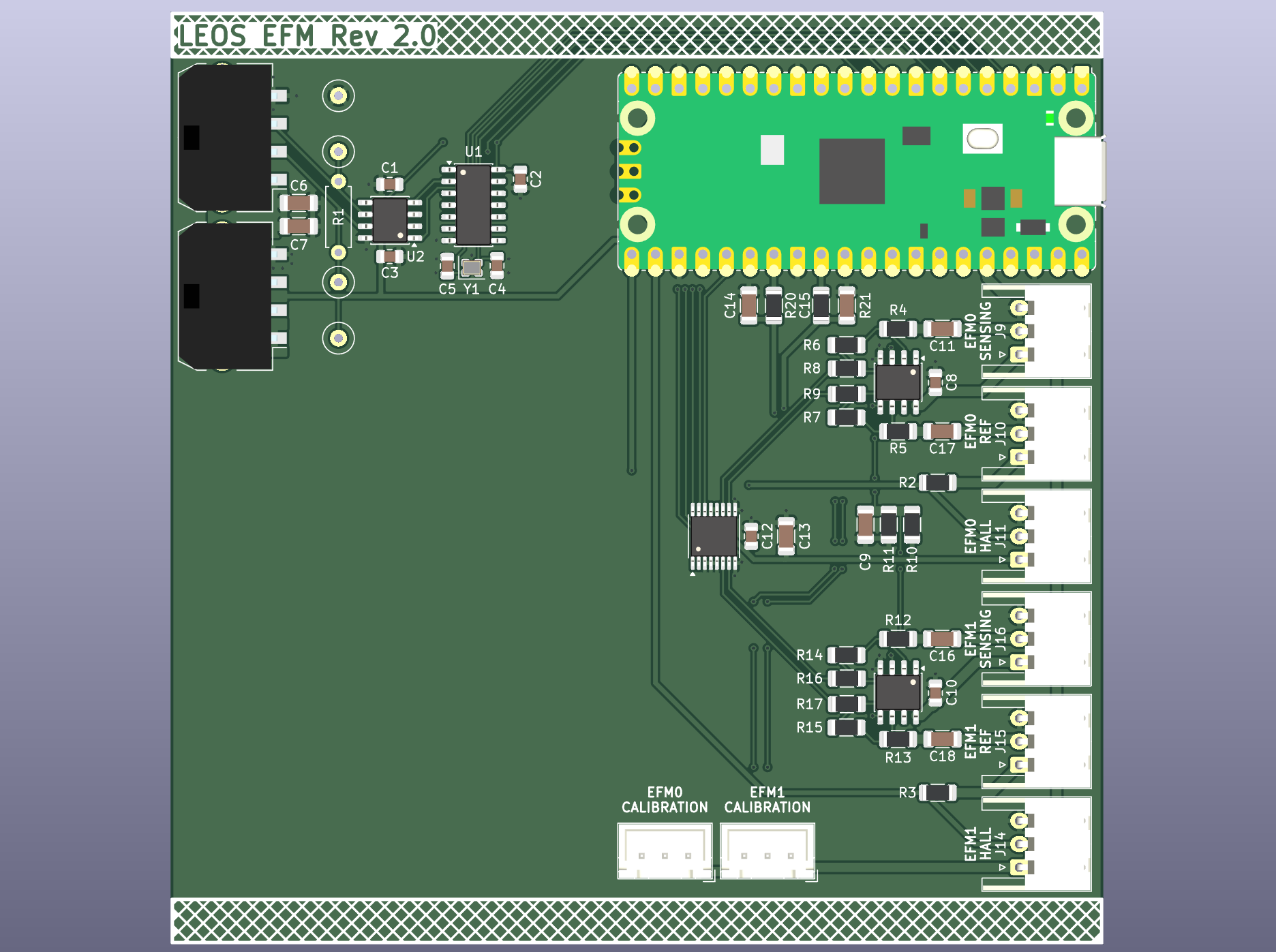
This repository is the starting-point PCB template for VIP Lightning From the Edge of Space (LEOS). All LEOS modules should be spun off from this template so that every module begins with the standard Raspberry Pi Pico, CAN-FD network, stack connectors, board shape, and mechanical layout.
Do not fork or clone this repository as the permanent home of a new module. Create a fresh repository from the public GitHub template instead:
LEOS-stack-template.kicad_pro in KiCad.GitHub also allows this template to be selected from the Repository template menu while creating a new repository. See GitHub's repository template instructions for the current interface.
| Qty | Value | Footprint | References |
|---|---|---|---|
| 8 | 10k | Resistor_SMD:R_1206_3216Metric | R2, R3, R4, R5, R12, R13, R20, R21 |
| 6 | 0.1u | Capacitor_SMD:C_0805_2012Metric | C1, C2, C3, C8, C10, C12 |
| 6 | S3B-XH-A-1 | Connector_JST:JST_XH_S3B-XH-A-1_1x03_P2.50mm_Horizontal | J9, J10, J11, J14, J15, J16 |
| 4 | 1M | Resistor_SMD:R_1206_3216Metric | R6, R7, R14, R15 |
| 4 | 3.3u | Capacitor_SMD:C_1206_3216Metric | C11, C16, C17, C18 |
| 4 | 33 | Resistor_SMD:R_1206_3216Metric | R8, R9, R16, R17 |
| 4 | 4.7u | Capacitor_SMD:C_1206_3216Metric | C9, C13, C14, C15 |
| 2 | 10p | Capacitor_SMD:C_0805_2012Metric | C4, C5 |
| 2 | 1k | Resistor_SMD:R_1206_3216Metric | R10, R11 |
| 2 | 22u | Capacitor_SMD:C_1206_3216Metric | C6, C7 |
| 2 | B3B-XH-A | Connector_JST:JST_XH_B3B-XH-A_1x03_P2.50mm_Vertical | J12, J13 |
| 2 | MicroFit_1x4 | LEOS:Molex_MicroFit3.0_43650-0410_1x04_Horizontal | J1, J2 |
| 2 | OPA2333AID | Package_SO:SOIC-8_3.9x4.9mm_P1.27mm | U3, U5 |
| 1 | 120 | Resistor_THT:R_Axial_DIN0207_L6.3mm_D2.5mm_P7.62mm_Horizontal | R1 |
| 1 | 40 MHz | Crystal:Crystal_SMD_2016-4Pin_2.0x1.6mm | Y1 |
| 1 | 5V Test Point | TestPoint:TestPoint_Loop_D2.60mm_Drill0.9mm_Beaded | TP3 |
| 1 | ADS1220IPW | Package_SO:TSSOP-16_4.4x5mm_P0.65mm | U4 |
| 1 | CAN-H Test Point | TestPoint:TestPoint_Loop_D2.60mm_Drill0.9mm_Beaded | TP1 |
| 1 | CAN-L Test Point | TestPoint:TestPoint_Loop_D2.60mm_Drill0.9mm_Beaded | TP2 |
| 1 | GND Test Point | TestPoint:TestPoint_Loop_D2.60mm_Drill0.9mm_Beaded | TP4 |
| 1 | MCP2518FD | Package_SO:SOIC-14_3.9x8.7mm_P1.27mm | U1 |
| 1 | MCP2562FD | Package_SO:SOIC-8_3.9x4.9mm_P1.27mm | U2 |
| 1 | RaspberryPi Pico | Module:RaspberryPi_Pico_Common_Unspecified | A1 |


VIP-LES/flight-computer-pcb
The flight computer PCB stack design. Started Fall '25


Tinkerbug-Robotics/TinkerRocket
Model rocket flight computer, ground station, iOS app, and simulation
It measures 100 × 100 mm and has 2 copper layers, 1.6 mm thick.
58 parts, built around the MCP2562FD-E/P, ADS1220IPW, OPA2333AID and MCP2518FDT-E/SL-HX. The full list of its parts is on this page, with links to each part's symbol and footprint where PCBKit's library has them.
From the VIP-LES/leos-efm-pcb repository on GitHub, at the commit this page was made from: the board is LEOS-efm.kicad_pcb and its schematic GAIN100stage.kicad_sch. PCBKit opens the board in the browser, with nothing to install.
Its repository states no licence, so its author keeps all rights: ask VIP-LES before reusing the design.