14MHz Accelerator V2 2
14MHz 68000 accelerator with 1MB fast ram for amiga 500
- Size
- 84 × 89 mm
- Copper layers
- 2
- Thickness
- 1.6 mm
- Parts
- 42
- Nets
- 98
- Pads
- 366
- Tracks, vias
- 1,878, 180
- Pours
- 4
- Routed
- Yes
- KiCad
- KiCad 4
- Created
- 30 Jun 2021
- Updated
- 1 Aug 2021
Overview
14MHz Accelerator V2 2 is an open-source printed circuit board by Mathesar, from the Mathesar/14mhz-accelerator repository on GitHub. It is a 2-layer board of 84 × 89 mm with 42 parts on 98 nets, routed with 1,878 tracks and 180 vias.
It is built around the 74ACT02M, 74ACT08SC and 74ACT11251D, with the 74ACT32PC, 74HCT4046AD and 74HCT74D among its other parts. Its parts include 17 capacitors, 11 ICs, 5 resistors and 3 connectors. It belongs with the retro computing and games boards of this library.
Main components
774ACT02M
SOIC-14SOIC-14 Specialty Logic ROHSSTMicroelectronicsSpecialty Logic74ACT08SC
SOIC-14-40℃~+85℃ 2 24mA 24mA 2V 3.76V、4.76V 4 4.5V~5.5V 440mV 4uA 74ACT Series 800mV 9ns@5V,50pF AND Gate SOIC-14 Logic Gates ROHSonsemiLogic Gates74ACT11251D
SOIC-16-40℃~+85℃ 24mA 24mA 4.5V~5.5V 5.2ns 74ACT 8uA Output enable high-impedance、Tri-state output SOIC-16 Signal Switches, Multiplexers, DecodersTexas InstrumentsSignal Switches, Multiplexers, Decoders74ACT32PC
DIP-14-40℃~+85℃ 2 24mA 24mA 2V 3.76V、4.76V 4 4.5V~5.5V 440mV 4uA 74ACT Series 800mV 9ns@5V,50pF OR Gate TTL Compatible CMOS DIP-14 Logic Gates ROHSonsemiLogic Gates74HCT4046AD
SOIC-16-40℃~+125℃ 4.5V~5.5V SOIC-16 Clock Generators, PLLs, Frequency Synthesizers ROHSNexperiaClock Generators / Frequency Synthesizers / PLL74HCT74D
SOIC-14-40℃~+125℃ 1 2 3.5pF 3ns 4.5V~5.5V 40uA 44ns@4.5V,50pF 4mA 4mA 59MHz 5ns 74HCT Series Asynchronous Complementary D-Type Rising Edge Set and Reset SO-14 Flip Flops ROHSNexperia74 SeriesTLC555CD
SOIC-80℃~+70℃ 2.1MHz 2V~15V 360uA SOIC-8 555 Timers / Counters ROHSTexas InstrumentsTimers / Counters
README
README.md14mhz-accelerator
This is 14MHz 68000 accelerator with 1MB fast ram and disable switch for the Amiga. Tested on a rev. 5 Amiga 500. It might also work on other revisions and Amiga models but that has not been tested. The design is licensed under CERN OHL-S V2.0
The design is a complete overhaul of a design by Livio Plos and Jorg Richter. Although based upon that design so much has been changed that it is almost like a new design.
Changes include:
- New clock doubler using an old school 4046 PLL to generate the 7MHz quadrature clock This is more reliable than the RC delays in the original design. Alternatively the quadrature clock can be taken from the motherboard. The latter has not been tested
- 3 input NOR's have been replaced by more common 2-input NOR's In the process the basic design could be reduced to 4 IC's.
- some JK flipflops have been replaced by D latches.
- The E vs VMA/VPA timing has been improved for more robust write timing
- AS is now delayed before being fed to the motherboard fixing issues when the CPU does a chipset cycle after a CIA cycle.
- an optional 1Mb of zero waitstate Ranger RAM has been added to take full advantage of the 14MHz cpu.
- an optional reset timing based switch has been added to disable the ranger RAM upon boot.
Variants
The accelerator can be build in 3 variant:
- Accelerator only This only doubles the clock of the CPU to 14MHz.
- Accelerator plus 1MB zero waitstate ranger RAM The above but adds 1MB of fast RAM. This makes the accelerator about 2.7 times faster than a stock A500
- Accelerator plus 1MB zero waitstate ranger RAM plus disable circuit The above but adds a timer based disable option for the RAM. By holdiing ctrl-amiga-amiga down for more than 5..6 seconds the RAM is disabled. It is enabled again on the next (less than 5..6 seconds) reset cycle
Building hints
- use turned/machined pins only for the host connector! The thick part is soldered on the accelerator, the thin part goes into the 68000 socket on the motherboard. Makes sure to use the full length of the pins (only solder the tips in the accelerator board) so the accelerator sits above the Kickstart.
- an MC68HC000 (HCMOS version) is preferred as it uses less power and has better drive. This might also help with EPROM Kickstarts on a rev. 5 motherboard.
- The PLL might needs some tuning to provide a 50% dutycycle clock. Tuning is done by making the value of R3 slightly smaller or larger until testpoint J2 shows a nice 50% / 14MHZ clock signal. An oscilloscope works best here but alternatively a simple multimeter can be used to adjust the DC voltage to read half the VCC value. (thus typically about 2.5V if VCC is really 5V)
- Alternatively the CDAC signal from the motherboard can be used. No tuning needed but untested at this point.
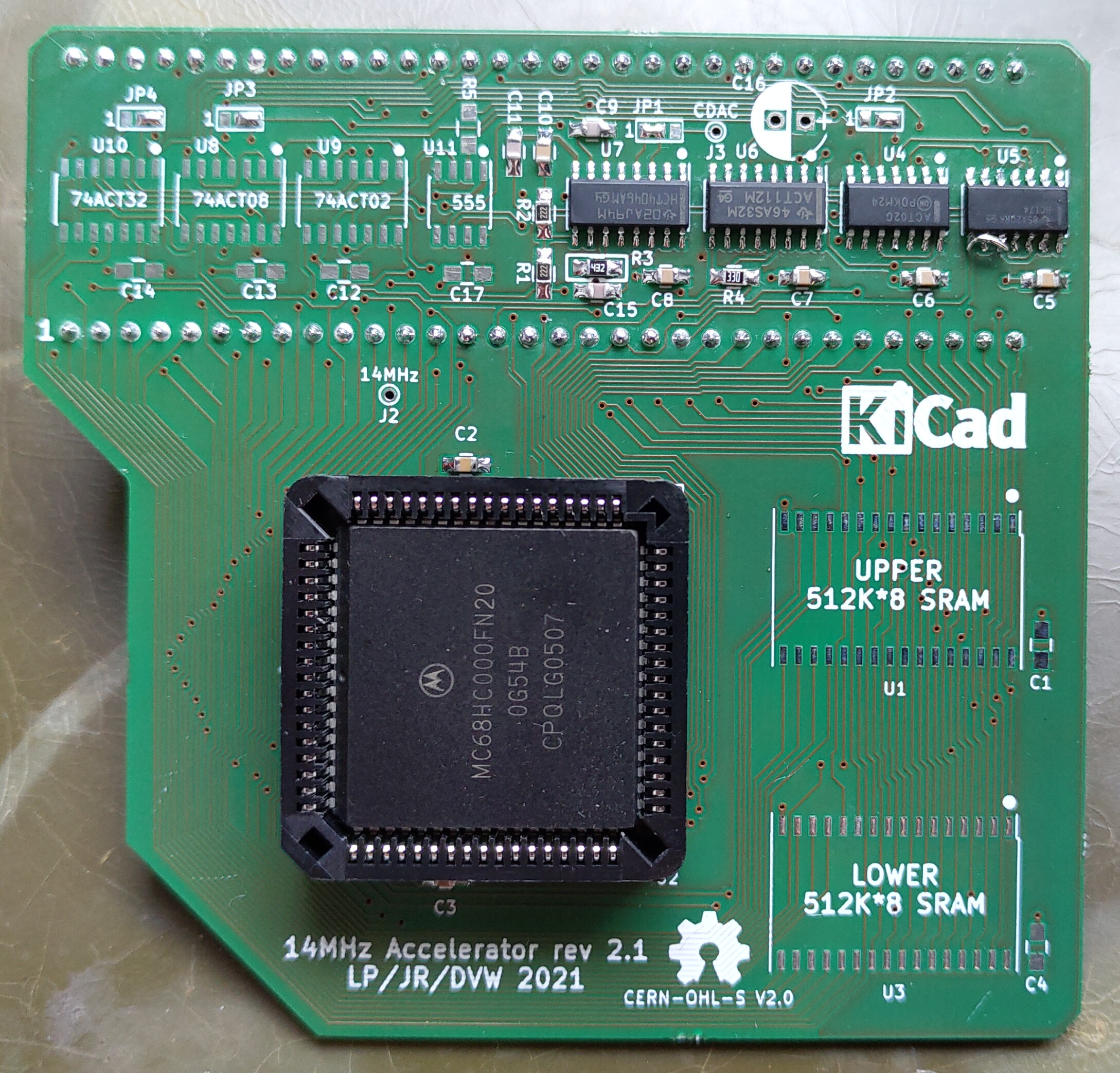
Here is a picture of the most basic variant (accelerator only) for reference purposes:

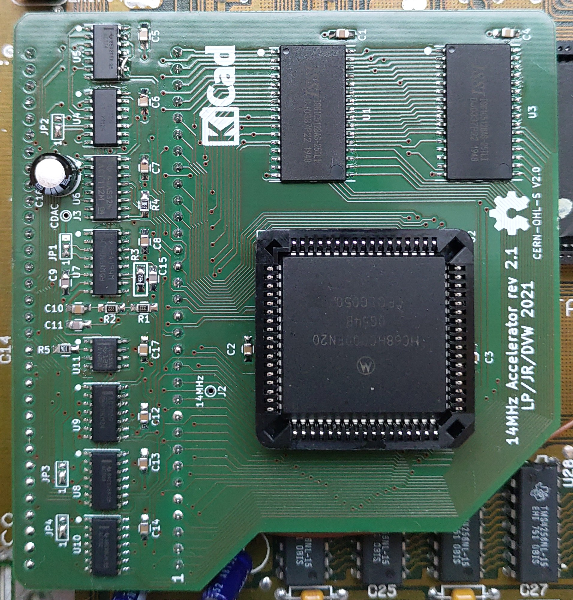
And here a picture of what a complete build should look like:

Have fun!
Parts
42| Qty | Value | Footprint | References |
|---|---|---|---|
| 13 | 100n | Capacitors_SMD:C_0805_HandSoldering | C1, C2, C3, C4, C5, C6, C7, C8, C10, C12, C13, C14, C17 |
| 4 | GS3 | Connectors:GS3 | JP1, JP2, JP3, JP4 |
| 2 | 100p | Capacitors_SMD:C_0805_HandSoldering | C9, C15 |
| 2 | 2K2 | Resistors_SMD:R_0805_HandSoldering | R1, R2 |
| 2 | 512K*8_SRAM | Housings_SSOP:TSOP-II-32_21.0x10.2mm_Pitch1.27mm | U1, U3 |
| 2 | 74ACT02 | Housings_SOIC:SOIC-14_3.9x8.7mm_Pitch1.27mm | U4, U9 |
| 1 | 100K | Resistors_SMD:R_0805_HandSoldering | R5 |
| 1 | 22p | Capacitors_SMD:C_0805_HandSoldering | C11 |
| 1 | 33 | Resistors_SMD:R_0805_HandSoldering | R4 |
| 1 | 47u/16V | Capacitors_THT:CP_Radial_D6.3mm_P2.50mm | C16 |
| 1 | 4K3 | Resistors_SMD:R_0805_HandSoldering | R3 |
| 1 | 68K_Host_Interface | Housings_DIP:DIP-64_W22.86mm | J1 |
| 1 | 74ACT08 | Housings_SOIC:SOIC-14_3.9x8.7mm_Pitch1.27mm | U8 |
| 1 | 74ACT112 | Housings_SOIC:SOIC-16_3.9x9.9mm_Pitch1.27mm | U6 |
| 1 | 74ACT32 | Housings_SOIC:SOIC-14_3.9x8.7mm_Pitch1.27mm | U10 |
| 1 | 74HCT4046 | Housings_SOIC:SOIC-16_3.9x9.9mm_Pitch1.27mm | U7 |
| 1 | 74HCT74 | Housings_SOIC:SOIC-14_3.9x8.7mm_Pitch1.27mm | U5 |
| 1 | CDAC IN | Connectors:PINTST | J3 |
| 1 | MC68HC000 | Kicad_modules:PLCC68_through_hole_socket | U2 |
| 1 | TEST_POINT | Connectors:PINTST | J2 |
| 1 | TLC555CD | Housings_SOIC:SOIC-8_3.9x4.9mm_Pitch1.27mm | U11 |
The 40 most common of 42 parts.
Similar boards
- 2 layers160 × 100 mm

- 2 layers118 × 50 mm

- 2 layers56.6 × 57.7 mm

TashTwenty Tiny
lampmerchant/tashtwenty
An interface for the DCD protocol used by Apple's Hard Disk 20.
31 parts35GPL-3.0 - 4 layers

6-Slot Backplane
transistorfet/retroverse
A collection of VME-based hardware and software for modular computers
136 parts17 - 4 layers401.3 × 203.2 mm

Cpu010
thorpej/pg68k
The 68k Playground, a 680x0-based home-brew computer with multiple CPU options
272 parts15 - 4 layers253 × 169.1 mm

- 2 layers65.5 × 58.4 mm

- 4 layers191 × 229 mm

Questions
How big is the 14MHz Accelerator V2 2 PCB?
It measures 84 × 89 mm and has 2 copper layers, 1.6 mm thick.
What parts does the 14MHz Accelerator V2 2 use?
42 parts, built around the 74ACT02M, 74ACT08SC, 74ACT11251D and 74ACT32PC. The full list of its parts is on this page, with links to each part's symbol and footprint where PCBKit's library has them.
Where can I download the 14MHz Accelerator V2 2 KiCad files?
From the Mathesar/14mhz-accelerator repository on GitHub, at the commit this page was made from: the board is hardware/14MHz_Accelerator_V2_2.kicad_pcb. PCBKit opens the board in the browser, with nothing to install.
Can I use the 14MHz Accelerator V2 2 design in my own project?
Its repository states no licence, so its author keeps all rights: ask Mathesar before reusing the design.