4 layers50 × 30 mm
Picodvi
Fr4nkFletcher/ESP32-Marauder-Cheap-Yellow-Display
ESP32Marauder Cheap Yellow Display
55 parts1.8kMIT

 Wren6991/PicoStation3D50
3D games console based on RP2040 and iCE40 UP5k
Picostation is an open-source printed circuit board by Wren6991, from the Wren6991/PicoStation3D repository on GitHub, published under the CC0-1.0 licence. It is a 4-layer board of 100 × 50 mm with 78 parts on 103 nets, routed with 628 tracks and 189 vias.
It is built around the RP2040, W25Q128JVSIQ and NCP115ASN330. Its parts include 31 capacitors, 26 resistors, 7 connectors, 5 ICs and 2 diodes. It belongs with the fPGA and programmable logic boards and the RP2040 and FPGA and CPLD boards of this library.


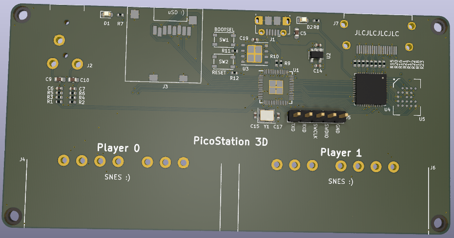
This is an unfinished, untested project to develop a 3D games console based on an RP2040 microcontroller and an iCE40 UP5k FPGA. Quick links:
From left to right, the components on the top edge are:
The bottom edge has two SNES controller sockets. Also on the board is an 8MiB HyperRAM connected to the FPGA.
There is a RESET and BOOTSEL button for the RP2040, for quick firmware updates over USB, but the debug header (UART + SWD) is a better solution for iterating and developing code.
There are 12 wires connecting the FPGA to the microcontroller, one of them going from a GPOUT clock output on the RP2040 to a GB_IN global clock input pin on the UP5k. The intention is to use these for an 8 bit parallel bus with a free-running clock, a valid-ready handshake and an IRQ line, and for the UP5k to derive its internal clocks from the bus clock. This interface overlaps with the pins required to load the FPGA's internal configuration memory (and the RP2040 also has control of the UP5k's reset) so there is no separate external flash required for the UP5k.
Run everything, including graphics routines, on RP2040, and use the UP5k as a parallel to DVI-D bridge -- see here for a quick demo of some scanline blitting on RP2040
Run everything, including a soft processor, on the UP5k, and use RP2040 as a surprisingly cost-effective USB-serial bridge, as well as for firmware upload. You'll need some kind of shell running on the RP2040 to provide audio and controller port access from the FPGA
Run game logic, audio, controller access and SD card access on RP2040, put all the graphics hardware in the UP5k (with the local 8MB HyperRAM as VRAM, plus the UP5k's internal 128k SPRAM)
Run 3D vertex-side operations on RP2040, and put 3D fragment-side hardware on the FPGA
I've laid out a first iteration of the board, and have soldered up a prototype, but haven't had the chance to bring up the board or write any firmware, thanks to being a bit overloaded with the launch of RP2040 itself!
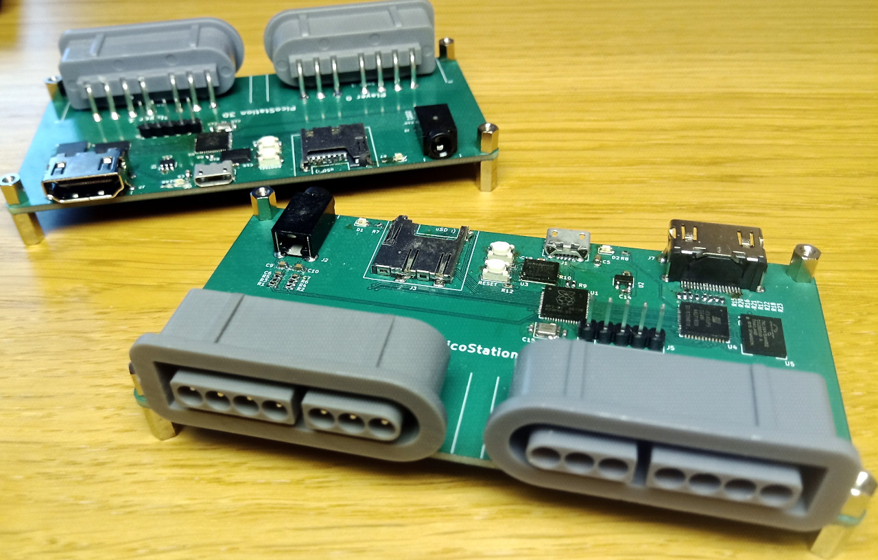
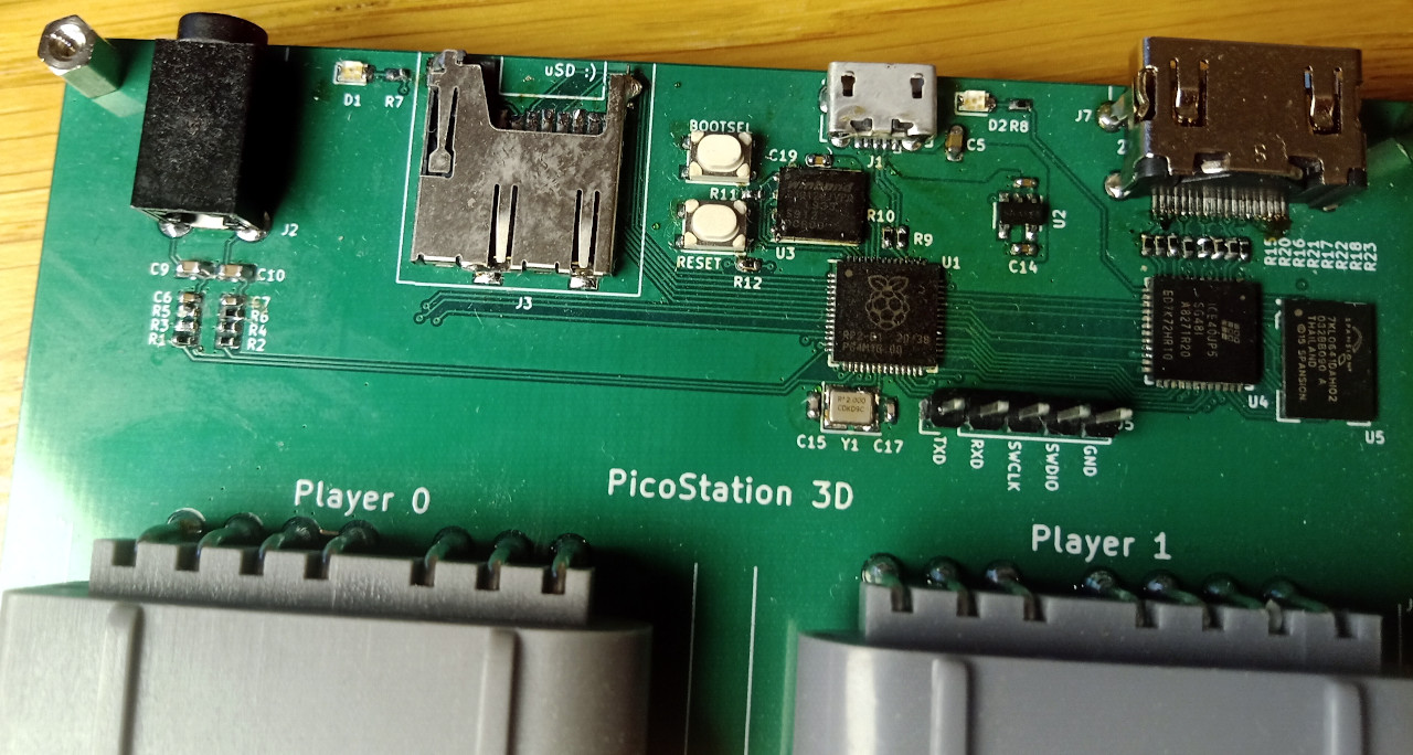
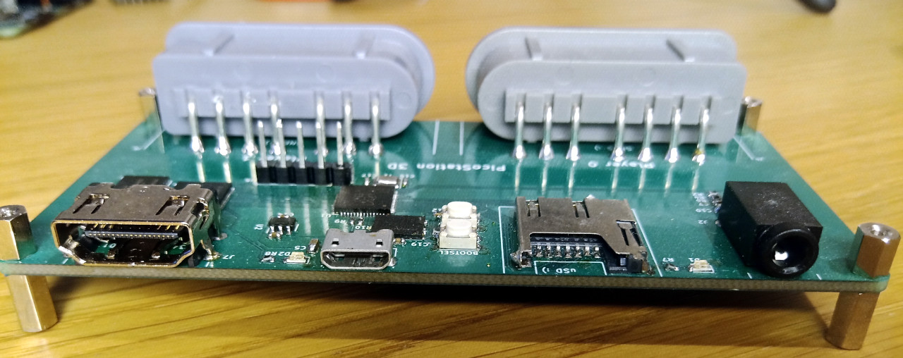
There are questionable decisions in the schematic (in particular the power chain violates the UP5k's sequencing requirements) so you shouldn't copy what you see here, but I'm posting this anyway because it might inspire somebody to make something better, and that is more important than me being embarrassed about my shoddy design work.
You can find a proof of concept for direct DVI output from a UP5k FPGA in this repo.
I've also managed to squeeze RISCBoy plus a DVI output onto a UP5k. Still need to push that code but you can see a video of it I tweeted. This shows you can fit plenty of interesting graphics hardware (and in this case a RISC-V processor) into a UP5k whilst generating DVI-D signals.
Known issues with rev A:
If you have read all the way to the end and you have spotted something else that irritates you about this design, please raise an issue! It will be a while until I get to Rev B. The main purpose of Rev A was to explore what I could get away with, and to develop the comms and interactions between microcontroller and FPGA.
| Qty | Value | Footprint | References |
|---|---|---|---|
| 18 | 100n | Capacitor_SMD:C_0402_1005Metric | C3, C4, C6, C11, C13, C19, C21, C22, C23, C24, C25, C26, C28, C29, C30, C31 +2 |
| 15 | 270 | Resistor_SMD:R_0402_1005Metric | R1, R2, R3, R4, R5, R6, R15, R16, R17, R18, R20, R21, R22, R23, R24 |
| 7 | 1u | Capacitor_SMD:C_0402_1005Metric | C1, C2, C12, C14, C16, C18, C20 |
| 7 | 2k2 | Resistor_SMD:R_0402_1005Metric | R7, R8, R11, R13, R14, R19, R26 |
| 4 | 10u | Capacitor_SMD:C_0603_1608Metric | C5, C9, C10, C27 |
| 2 | 10p | Capacitor_SMD:C_0402_1005Metric | C15, C17 |
| 2 | 27 | Resistor_SMD:R_0402_1005Metric | R9, R10 |
| 2 | LED | LED_SMD:LED_0603_1608Metric | D1, D2 |
| 2 | PTS815 | picostation:SW_SPST_PTS815 | SW1, SW2 |
| 1 | 100 | Resistor_SMD:R_0402_1005Metric | R25 |
| 1 | AudioJack3 | picostation:STX-3000-TRS | J2 |
| 1 | Conn_01x05 | Connector_PinHeader_2.54mm:PinHeader_1x05_P2.54mm_Vertical | J5 |
| 1 | Micro_SD_Card | picostation:MEM2061-MICRO-SD | J3 |
| 1 | NCP115ASN330 | Package_TO_SOT_SMD:SOT-23-5 | U2 |
| 1 | NF | Resistor_SMD:R_0402_1005Metric | R12 |
| 1 | NOT_HDMI_A | picostation:HDMI-SS-53000 | J7 |
| 1 | RH100-12.000 | Crystal:Crystal_SMD_3225-4Pin_3.2x2.5mm | Y1 |
| 1 | RP2040 | picostation:QFN-56_EP_7x7_Pitch0.4mm | U1 |
| 1 | S70KS128 | picostation:S70KS128 | U5 |
| 1 | SNES | picostation:SNES-Controller-Left | J6 |
| 1 | SNES | picostation:SNES-Controller-Right | J4 |
| 1 | USB_B_Micro | Connector_USB:USB_Micro-B_Molex-105017-0001 | J1 |
| 1 | W25Q128JV | Package_SON:WSON-8-1EP_6x5mm_P1.27mm_EP3.4x4mm | U3 |
| 1 | iCE40UP5k-QFN48 | Package_DFN_QFN:QFN-48-1EP_7x7mm_P0.5mm_EP5.3x5.3mm | U4 |
The 74 most common of 78 parts.
Fr4nkFletcher/ESP32-Marauder-Cheap-Yellow-Display
ESP32Marauder Cheap Yellow Display


shanteacontrols/OpenDeck
A platform for building interactive control and sensing devices using MIDI and OSC built with Zephyr RTOS.


polpo/picogus
Emulation of ISA sound cards and CD-ROM on Raspberry Pi Pico (GUS, SB/Adlib, MPU-401, Tandy, CMS, Panasonic CD-ROM) with USB mouse/joystick support

Bastardkb/Dilemma
The Dilemma is a vertical stagger low-profile keyboard with mods.
It measures 100 × 50 mm and has 4 copper layers, 1.6 mm thick.
78 parts, built around the RP2040, W25Q128JVSIQ and NCP115ASN330. The full list of its parts is on this page, with links to each part's symbol and footprint where PCBKit's library has them.
From the Wren6991/PicoStation3D repository on GitHub, at the commit this page was made from: the board is board/picostation.kicad_pcb. PCBKit opens the board in the browser, with nothing to install.
Its repository publishes it under the CC0-1.0 licence: you may reuse it on that licence's terms (keep the author's notice, and for a copyleft licence share your changes alike).