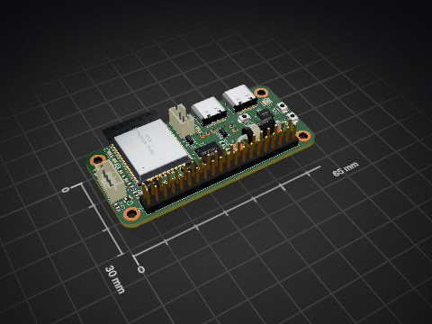
4 layers45.7 × 76.2 mm
Node v5 0 0
VTC-WISDOM/node_hardware
Schematic/PCB designs for WiSDOM nodes, also includes a few other related hardware projects
107 parts2CERN-OHL-W-2.0

 VTC-WISDOM/node_hardware2
Schematic/PCB designs for WiSDOM nodes, also includes a few other related hardware projects
Node v5 0 0 is an open-source printed circuit board by VTC-WISDOM, from the VTC-WISDOM/node_hardware repository on GitHub, published under the CERN-OHL-W-2.0 licence. It is a 4-layer board of 45.7 × 76.2 mm with 103 parts on 125 nets, routed with 84 tracks and 8 vias.
It is built around the RP2040, SIM7080G and W25Q128JVSIQ, with the AP2112K-3.3, MAX31342EWA+T and DMG2301L among its other parts. Its parts include 46 capacitors, 19 resistors, 13 ICs, 8 connectors and 3 diodes. It belongs with the RP2040 boards of this library.


a collection of schematic and pcb designs for the WiSDOM node unless otherwise specified, everything contained in this repository is licensed under the CERN Open Hardware License version 2 - Weakly Reciprocal License (CERN-OHL-W). this is comparable to the gpl2, see LICENSE for details
using your favorite package manager, install kicad-footprints and kicad-symbols alongside kicad. this is the best way to get the standard libraries. if you for some reason cannot do so, see the linked official kicad libraries in kicad-libs/footprints and kicad-libs/symbols. in the kicad symbol editor, go to preferences -> manage symbol libraries and select "add existing", navigate to the kicad-libs/symbols directory and select the symbol libraries contained therein. repeat this with the symbols contained in kicad-libs/JLCPCB-Kicad-Library. repeat this for footprints.
stores all of the relevant design files for the WiSDOM node that is based on the RP2040
like above but the RP2350
test projects, antenna and transmission equipment, etc. anything unspecified
will add as much documentation as possible!
changes:
SIM7080G NON-FUNCTIONAL
change since previous version:
| Qty | Value | Footprint | References |
|---|---|---|---|
| 18 | 0.1u | Capacitor_SMD:C_0402_1005Metric_Pad0.74x0.62mm_HandSolder | C1, C2, C3, C4, C5, C6, C7, C10, C11, C12, C18, C28, C30, C37, C38, C44 +2 |
| 9 | 10u | Capacitor_SMD:C_0805_2012Metric_Pad1.18x1.45mm_HandSolder | C13, C15, C17, C23, C24, C29, C31, C45, C46 |
| 6 | 1u | Capacitor_SMD:C_0805_2012Metric_Pad1.18x1.45mm_HandSolder | C14, C16, C25, C26, C27, C41 |
| 4 | 33p | Capacitor_SMD:C_0402_1005Metric_Pad0.74x0.62mm_HandSolder | C34, C35, C36, C43 |
| 4 | MountingHole_Pad | MountingHole:MountingHole_2.2mm_M2_Pad_TopBottom | H1, H2, H3, H4 |
| 3 | 100u | Capacitor_SMD:C_0805_2012Metric_Pad1.18x1.45mm_HandSolder | C39, C40, C42 |
| 3 | 10k | Resistor_SMD:R_0805_2012Metric_Pad1.20x1.40mm_HandSolder | R8, R10, R19 |
| 3 | 22 | Capacitor_SMD:C_0805_2012Metric_Pad1.18x1.45mm_HandSolder | R11, R12, R13 |
| 2 | 10k DNF | Resistor_SMD:R_0402_1005Metric_Pad0.72x0.64mm_HandSolder | R14, R15 |
| 2 | 15pF | Capacitor_SMD:C_0402_1005Metric_Pad0.74x0.62mm_HandSolder | C19, C20 |
| 2 | 1k | Resistor_SMD:R_0805_2012Metric_Pad1.20x1.40mm_HandSolder | R5, R7 |
| 2 | 27.4 | Resistor_SMD:R_0603_1608Metric_Pad0.98x0.95mm_HandSolder | R1, R2 |
| 2 | 4.7u | Capacitor_SMD:C_0805_2012Metric_Pad1.18x1.45mm_HandSolder | C21, C22 |
| 2 | 470k | Resistor_SMD:R_0805_2012Metric_Pad1.20x1.40mm_HandSolder | R17, R18 |
| 2 | 5.1k | Resistor_SMD:R_0805_2012Metric_Pad1.20x1.40mm_HandSolder | R3, R4 |
| 2 | 6p | Capacitor_SMD:C_0603_1608Metric_Pad1.08x0.95mm_HandSolder | C32, C33 |
| 2 | Conn_01x02_Pin | Connector_JST:JST_PH_B2B-PH-K_1x02_P2.00mm_Vertical | J1, J8 |
| 2 | DMG2301L | Package_TO_SOT_SMD:SOT-23 | Q1, Q2 |
| 2 | PTS526 SK15 SMTR2 LFS | WiSDOM:PTS526 | U7, U8 |
| 2 | SS14 | Diode_SMD:D_SMA | D2, D3 |
| 1 | logos:github_qr | LOGO | |
| 1 | logos:qrcode | LOGO | |
| 1 | 1042240820 | WiSDOM:1042240820_MOL | U11 |
| 1 | 12402012E212A | WiSDOM:AMPHENOL_12402012E212A | J2 |
| 1 | 22 | Resistor_SMD:R_0805_2012Metric_Pad1.20x1.40mm_HandSolder | R16 |
| 1 | 2k | Resistor_SMD:R_0805_2012Metric_Pad1.20x1.40mm_HandSolder | R6 |
| 1 | AP2112K-3.3 | Package_TO_SOT_SMD:SOT-23-5 | U3 |
| 1 | CAT24M01W | Package_SO:SOIC-8_3.9x4.9mm_P1.27mm | U12 |
| 1 | CAT3200-5 | Package_TO_SOT_SMD:SOT-23-6 | U4 |
| 1 | Conn_02x02_Odd_Even | Connector_PinHeader_2.54mm:PinHeader_2x02_P2.54mm_Vertical | J5 |
| 1 | Conn_02x08_Odd_Even | Connector_PinHeader_2.54mm:PinHeader_2x08_P2.54mm_Vertical | J4 |
| 1 | Conn_Coaxial | Connector_Coaxial:SMA_Samtec_SMA-J-P-H-ST-EM1_EdgeMount | J3 |
| 1 | GNSS_ANT | WiSDOM:CONN_CONMHF1-SMD_LNX | J6 |
| 1 | L | Inductor_SMD:L_0402_1005Metric_Pad0.77x0.64mm_HandSolder | L1 |
| 1 | LED | LED_SMD:LED_1206_3216Metric_Pad1.42x1.75mm_HandSolder | D1 |
| 1 | LOGO | WiSDOM:prince | G*** |
| 1 | LOGO | logos:wisdom_logo_lineborder | G*** |
| 1 | MAX31342EWA+T | WiSDOM:21-100291_W80D&plus_1_MXM | U13 |
| 1 | MCP73831-2-OT | Package_TO_SOT_SMD:SOT-23-5 | U5 |
| 1 | MCP7940 / DS1307 / PCF8523 | Package_SO:SOIC-8_3.9x4.9mm_P1.27mm | U10 |
| 1 | R | Resistor_SMD:R_0805_2012Metric_Pad1.20x1.40mm_HandSolder | R9 |
| 1 | RFM69HCW | RF_Module:HOPERF_RFM9XW_SMD | U6 |
| 1 | RF_ANT | WiSDOM:CONN_CONMHF1-SMD_LNX | J7 |
| 1 | RP2040 | RP2040_minimal_r2:RP2040-QFN-56 | U1 |
| 1 | RTC_BAT | WiSDOM:BAT_BAT-HLD-001-THM | BT1 |
| 1 | SC32S-7PF20PPM | WiSDOM:XTAL_SC32S-7PF20PPM_EPS | XTAL1 |
| 1 | SIM7080G | WiSDOM:XCVR_SIM7080G | U9 |
| 1 | W25Q128JVS | Package_SO:SOIC-8_5.23x5.23mm_P1.27mm | U2 |
| 1 | ~ | WiSDOM:XTAL-445 | X1 |
It measures 45.7 × 76.2 mm and has 4 copper layers, 1.6 mm thick.
103 parts, built around the RP2040, SIM7080G, W25Q128JVSIQ and AP2112K-3.3. The full list of its parts is on this page, with links to each part's symbol and footprint where PCBKit's library has them.
From the VTC-WISDOM/node_hardware repository on GitHub, at the commit this page was made from: the board is node-rp2040/node_v5_0_0/node_v5_0_0_.kicad_pcb and its schematic antennas/915-yagi/915-yagi-v2/yagi/yagi.kicad_sch. PCBKit opens the board in the browser, with nothing to install.
Its repository publishes it under the CERN-OHL-W-2.0 licence: you may reuse it on that licence's terms (keep the author's notice, and for a copyleft licence share your changes alike).
VTC-WISDOM/node_hardware
Schematic/PCB designs for WiSDOM nodes, also includes a few other related hardware projects

VTC-WISDOM/node_hardware
Schematic/PCB designs for WiSDOM nodes, also includes a few other related hardware projects

VTC-WISDOM/node_hardware
Schematic/PCB designs for WiSDOM nodes, also includes a few other related hardware projects

VTC-WISDOM/node_hardware
Schematic/PCB designs for WiSDOM nodes, also includes a few other related hardware projects

VTC-WISDOM/node_hardware
Schematic/PCB designs for WiSDOM nodes, also includes a few other related hardware projects

VTC-WISDOM/node_hardware
Schematic/PCB designs for WiSDOM nodes, also includes a few other related hardware projects


OklahomaOpenSourceHardware/OKC-OSH-2024-Badge
2024 badge for Oklahoma PCB Tech Conferences


OpenJBOD/rp2040
This repository contains the hardware design files OpenJBOD RP2040 Baseboard.

rein-baremetal/REIN_R1_KiCad
Dual-MCU baremetal embedded development board featuring high-speed QSPI storage, hardware USB hub, and flexible power management. Open for PCB trace routing collaboration