
2 layers107 × 54 mm

 vishalbodkhe/555-Timer-LED-Blinker-PCB
555 Timer LED Blinker PCB designed using KiCad
555-Timer LED Blinker PCB is an open-source printed circuit board by vishalbodkhe, from the vishalbodkhe/555-Timer-LED-Blinker-PCB repository on GitHub. It is a 2-layer board of 42 × 18 mm with 8 parts on 8 nets, routed with 68 tracks and 0 vias.
It is built around the NE555D. Its parts include 3 resistors, 2 capacitors, 1 IC, 1 diode and 1 connector.
A 555 Timer based LED Blinker PCB designed using KiCad.
This project is a simple LED blinker circuit using the NE555 timer IC in astable mode.
The complete PCB design workflow was performed using KiCad, including:
| Reference | Component | Value |
|---|---|---|
| U1 | NE555 Timer IC | NE555D |
| R1 | Resistor | 1kΩ |
| R2 | Resistor | 10kΩ |
| R3 | Resistor | 330Ω |
| C1 | Capacitor | 10µF |
| C2 | Capacitor | 100nF |
| D1 | LED | LED |
| J1 | Screw Terminal | 2-Pin |
The NE555 timer is configured in astable mode to generate a continuous square-wave output.
The output of the 555 timer drives the LED through a 330Ω current-limiting resistor.
The PCB was designed and routed using KiCad.
The board includes:
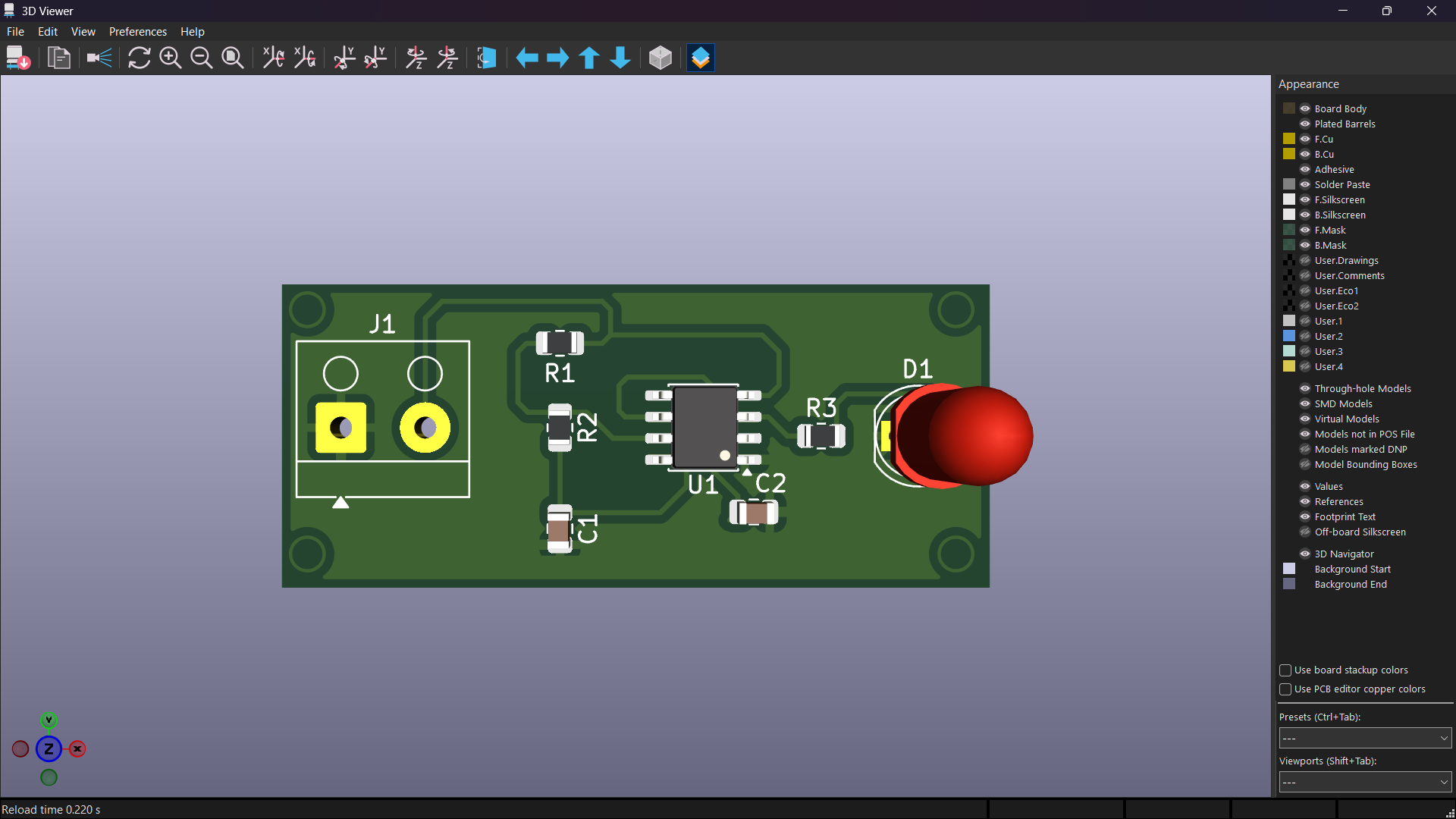
Gerber files required for PCB fabrication are included in this repository.
Included fabrication files:
p2.kicad_sch — Schematicp2.kicad_pcb — PCB Layoutp2.kicad_pro — KiCad Projectp2-F_Cu.gbrp2-B_Cu.gbrp2-F_Mask.gbrp2-B_Mask.gbrp2-F_Silkscreen.gbrp2-B_Silkscreen.gbrp2-Edge_Cuts.gbrp2-PTH.drlp2-NPTH.drlThrough this project, I learned and practiced:
Completed
Schematic → PCB Layout → Routing → DRC → 3D Verification → Gerber Generation
Vishal Bodkhe
Electronics & Computer Engineering
This project is created for educational and portfolio purposes.
| Qty | Value | Footprint | References |
|---|---|---|---|
| 1 | 100nF | Capacitor_SMD:C_0805_2012Metric | C2 |
| 1 | 10k | Resistor_SMD:R_0805_2012Metric | R2 |
| 1 | 10uF | Capacitor_SMD:C_0805_2012Metric | C1 |
| 1 | 1k | Resistor_SMD:R_0805_2012Metric | R1 |
| 1 | 330 | Resistor_SMD:R_0805_2012Metric | R3 |
| 1 | LED | LED_THT:LED_D5.0mm | D1 |
| 1 | NE555D | Package_SO:SOIC-8_3.9x4.9mm_P1.27mm | U1 |
| 1 | Screw_Terminal_01x02 | TerminalBlock_Altech:Altech_AK100_1x02_P5.00mm | J1 |

Millisman/EG8010
Collection of designs for the EG8010 (ASIC for single-phase SPWM control H-bridge)

Andre1Becker/GalvOS
Open-source ESP32-S3 laser show controller — built to replace proprietary OEM controllers in RGB galvo laser projectors


Robert-Mones/Claculator
A reverse Polish notation calculator with added features such as comparisons, branching, and custom recursive operators taken from the Clac project from the 15-122 course at Carnegie Mellon University.

It measures 42 × 18 mm and has 2 copper layers, 1.6 mm thick.
8 parts, built around the NE555D. The full list of its parts is on this page, with links to each part's symbol and footprint where PCBKit's library has them.
From the vishalbodkhe/555-Timer-LED-Blinker-PCB repository on GitHub, at the commit this page was made from: the board is p2.kicad_pcb and its schematic p2.kicad_sch. PCBKit opens the board in the browser, with nothing to install.
Its repository states no licence, so its author keeps all rights: ask vishalbodkhe before reusing the design.