
2 layers107 × 54 mm
 ben5049/ICRS-PCB-Ruler3
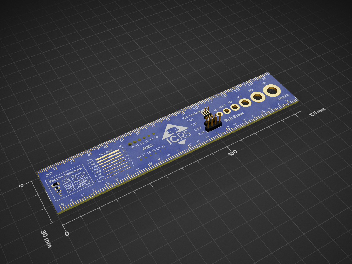
ICRS PCB ruler
Ruler V2 KiCad is an open-source printed circuit board by ben5049, from the ben5049/ICRS-PCB-Ruler repository on GitHub, published under the Apache-2.0 licence. It is a 2-layer board of 155 × 30 mm with 38 parts on 20 nets, routed with 93 tracks and 2 vias.
It is built around the NE555D. Its parts include 10 diodes, 3 resistors, 2 ICs, 1 capacitor and 1 connector.
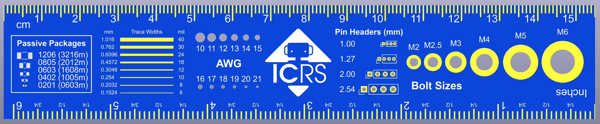
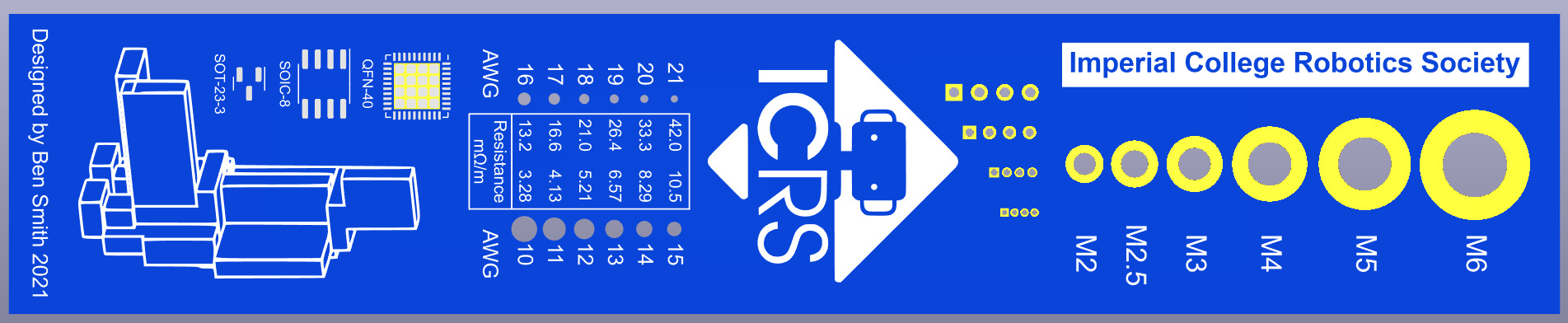
A 15cm PCB ruler designed for Imperial College Robotics Society. It can be easily adapted/rebranded using the KiCad project in this repository.
Front:
Back:
To open this project in KiCad 7.0 clone this repository and open the .kicad_pro file in Ruler_KiCad. Next open the PCB editor and go to Preferences > Manage Footprint Libraries > Add Existing (the folder icon below the list of libraries). Then navigate to Ruler_KiCad/ruler_footprints and click "select folder". This is in order to get the custom footprints used in this project.
The gerber files needed for ordering can be found in Ruler_gerbers.zip. Simply upload this .zip file to any PCB manufacturer's website.
The recommended specifications for ordering this PCB are as follows:
Using JLCPCB's pricing, the cost of ordering x number of boards has been plotted in Pricing.xlsx.
| Qty | Value | Footprint | References |
|---|---|---|---|
| 10 | LED_Small | LED_SMD:LED_0402_1005Metric | D101, D102, D103, D104, D105, D106, D107, D108, D109, D110 |
| 2 | 1k | Resistor_SMD:R_0402_1005Metric | R101, R102 |
| 1 | 1u | Capacitor_SMD:C_0402_1005Metric | C101 |
| 1 | 4017 | Package_SO:SOP-16_3.9x9.9mm_P1.27mm | U102 |
| 1 | 47k | Resistor_SMD:R_0402_1005Metric | R103 |
| 1 | LOGO | ruler_footprints:Alert 40mm | G*** |
| 1 | LOGO | ruler_footprints:ICRS_20mm | G*** |
| 1 | LOGO | ruler_footprints:ICRS_28mm | G*** |
| 1 | NE555D | Package_SO:SOIC-8_3.9x4.9mm_P1.27mm | U101 |
| 1 | USB_C_Receptacle_PowerOnly_6P | Connector_USB:USB_C_Receptacle_GCT_USB4135-GF-A_6P_TopMnt_Horizontal | J102 |
The 20 most common of 38 parts.

Millisman/EG8010
Collection of designs for the EG8010 (ASIC for single-phase SPWM control H-bridge)

Andre1Becker/GalvOS
Open-source ESP32-S3 laser show controller — built to replace proprietary OEM controllers in RGB galvo laser projectors


Robert-Mones/Claculator
A reverse Polish notation calculator with added features such as comparisons, branching, and custom recursive operators taken from the Clac project from the 15-122 course at Carnegie Mellon University.

marove2000/UniBadge-9x9
A simple Badge PCP with 9x9 LEDs. Create symbols, figures, pxiel-art by just soldering LEDs to the spots you want. No programming needed.
It measures 155 × 30 mm and has 2 copper layers, 1.6 mm thick.
38 parts, built around the NE555D. The full list of its parts is on this page, with links to each part's symbol and footprint where PCBKit's library has them.
From the ben5049/ICRS-PCB-Ruler repository on GitHub, at the commit this page was made from: the board is Ruler_V2_KiCad/Ruler_V2_KiCad.kicad_pcb and its schematic Ruler_KiCad/Ruler_KiCad.kicad_sch. PCBKit opens the board in the browser, with nothing to install.
Its repository publishes it under the Apache-2.0 licence: you may reuse it on that licence's terms (keep the author's notice, and for a copyleft licence share your changes alike).