2 layers93.2 × 99.1 mm
Panelized
unicab369/ESP-MESS
I am building a Wireless Bridge System that can manage multiple devices using a variety of wireless technologies.
1,643 parts
 unicab369/ESP-MESS
I am building a Wireless Bridge System that can manage multiple devices using a variety of wireless technologies.
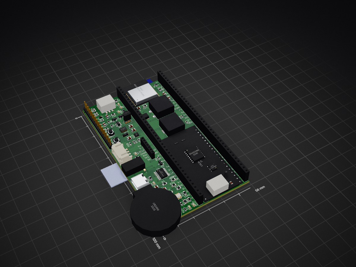
Sensor node is an open-source printed circuit board by unicab369, from the unicab369/ESP-MESS repository on GitHub. It is a 2-layer board of 58 × 100 mm with 106 parts on 175 nets, routed with 1,729 tracks and 211 vias.
It is built around the CH32V003F4P6, E18-MS1-PCB and ESP-12F, with the ESP32-C3-WROOM-02-H4, APDS-9960 and BH1750FVI-TR among its other parts. Its parts include 49 resistors, 18 ICs, 11 capacitors, 9 diodes and 9 connectors. It belongs with the home automation and IoT and sensors and measurement boards and the ESP32, ESP8266 and RISC-V boards of this library.


ESP-MESS is an open-source firmware for ESP8266 and ESP32 microcontrollers, enabling
rapid IoT prototyping for home automation, smart farming, smart business, and more.
Back in 2020 during Covid, I got an opportunity to look back and decide on what I want to do next. I thought about what I liked as a kid so I decided to build a remote control car. During my search for a suitable microcontroller, I stumbled upon the NodeMcu, a development board that house the ESP8266 module. Initially underestimating its capabilities, I soon realized its potential. Since then, my journey has led me to acquire skills in soldering, basic electronics, embedded programming, web development for microcontrollers, PCB design, and various wireless communication technologies.
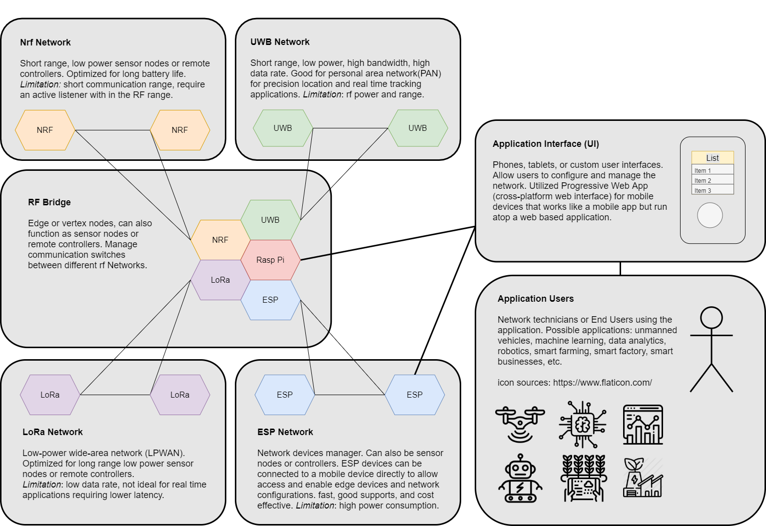
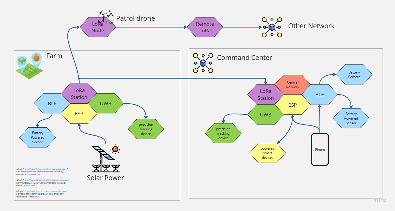
I am building a Wireless Bridge System that can manage multiple devices using a variety of wireless technologies. The system is designed to be flexible and scalable, allowing it to adapt to different wireless application requirements. My goal is to explore and discover different IoT applications while keeping the cost minimal. To achieve this, I created ESP-MESS.
Because it's cool. It's very cool. Ok, seriously, different wireless technologies have their own unique advantages and disadvantages. For instance, LoRa technology allows devices to communicate with each other over long distances, which is not possible with WiFi or Bluetooth. However, LoRa has a low data rate, which makes it unsuitable for transmitting large amounts of data such as videos or audios. On the other hand, UWB (Ultra Wide Band) technology has a short range but enables devices to be accurately positioned relative to another device. WiFi can stream a lot more data over the air compared to Bluetooth, but at the cost of higher power consumption, making it less suitable for battery-operated devices than Bluetooth or BLE. These are just a few examples of the advantages and disadvantages of different wireless technologies.
A Wireless Bridge System offers a versatile solution by allowing the integration of diverse wireless technologies to address various challenges. Users can enhance their networks by adding supported modules to the bridge, taking advantage of the strengths of each wireless technology. This flexibility empowers users to tailor custom wireless networks to fulfill specific needs, whether it's creating a wireless sensor network, a smart home automation system, a mesh network for industrial automation, or a communication system for autonomous vehicles. The system facilitates the extension, management, monitoring, and control of device networks. ESP-MESS is an implementation of this system, it offers carefully chosen supporting devices that balance performance and cost, enabling users to choose components that align with their requirements and budgets.
checkout our discord channel: https://discord.com/channels/793348436475904022/858758498875342878
A Live ESP-MESS Node: This is an ESP-MESS Node that runs on a Lithium-ion 18650 battery and a solar panel. The device records the temperature, humidity, ambient light level, battery voltage level, and the charging current from a solar panel. It utilizes ESP-Now to send signals to another Node, which is connected to my WiFi network. This Node publishes the readings to IoTPlotter for storage and data analysis. https://iotplotter.com/user/feed/627987619219815565
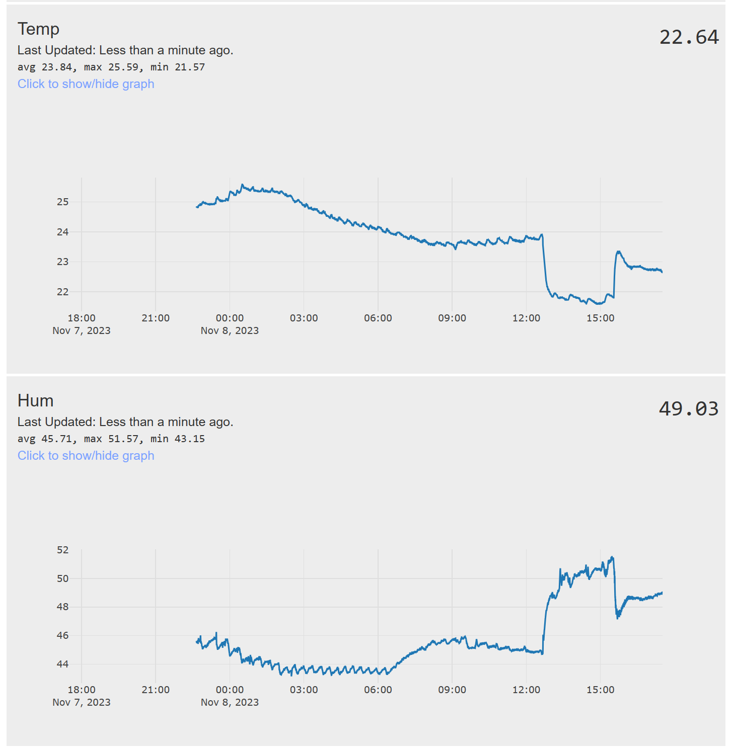
Right now it's functional but I have not finished document the setup. I will try to make a video with instructions on how to work it.
Currently I have got ESP-Now working and some works for the LoRa communication has been completed. Next step is to refine the ESP-Now, LoRa, and then add support for BLE.
Currently, I'm testing a few BLE modules. I'm trying to measure the power consumption of different devices and compare them with each other. This way I can pick one that I think is best suited for a low power device that can monitor multiple sensor nodes and can last on a battery for the minimum of 1 year.
make all monitor
| Qty | Value | Footprint | References |
|---|---|---|---|
| 30 | R | Resistor_SMD:R_0805_2012Metric | R1, R2, R3, R10, R12, R13, R14, R15, R16, R17, R18, R23, R25, R26, R30, R35 +14 |
| 18 | R | Resistor_SMD:R_0603_1608Metric | R4, R5, R11, R19, R20, R21, R22, R27, R28, R29, R31, R32, R33, R34, R36, R37 +2 |
| 11 | C | Capacitor_SMD:C_0805_2012Metric | C1, C2, C3, C4, C5, C6, C7, C8, C9, C10, C12 |
| 7 | LED | LED_SMD:LED_0603_1608Metric | D1, D3, D4, D7, D8, D9, D11 |
| 3 | Si2371EDS | Package_TO_SOT_SMD:SOT-23 | Q1, Q2, Q3 |
| 2 | Conn_01x39_Socket | Connector_PinSocket_2.54mm:PinSocket_1x39_P2.54mm_Vertical | J1, J4 |
| 2 | S3B-PH-SM4-TB | S3B-PH:JST_S3B-PH-SM4-TB | P1, P3 |
| 2 | SW_Push | Button_Switch_SMD:SW_SPST_PTS810 | SW1, SW3 |
| 1 | APDS-9960 | Sensor:Avago_APDS-9960 | U12 |
| 1 | BH1750FVI-TR | BH1750:XDCR_BH1750FVI-TR | U17 |
| 1 | CH32V003F4P6 | Package_SO:TSSOP-20_4.4x6.5mm_P0.65mm | U4 |
| 1 | CR2450 | Battery:BatteryHolder_ComfortableElectronic_CH273-2450_1x2450 | U3 |
| 1 | Conn_01x07_Pin | Connector_PinSocket_2.00mm:PinSocket_1x07_P2.00mm_Vertical | J6 |
| 1 | Conn_01x15_Pin | Connector_PinHeader_2.54mm:PinHeader_1x15_P2.54mm_Vertical | J5 |
| 1 | Crystal | Crystal:Crystal_Round_D1.5mm_Vertical | Y1 |
| 1 | Crystal | Crystal:Crystal_SMD_3215-2Pin_3.2x1.5mm | Y2 |
| 1 | DS1307Z+ | Package_SO:SOIC-8_3.9x4.9mm_P1.27mm | U15 |
| 1 | DS3231M | Package_SO:SOIC-16W_7.5x10.3mm_P1.27mm | U16 |
| 1 | D_Schottky | Diode_SMD:D_SOD-323 | D2 |
| 1 | E18-MS1-PCB | RF_Module:E18-MS1-PCB | U9 |
| 1 | ESP-12F | A_SensorNode:ESP12_SMD | U10 |
| 1 | ESP32-C3-WROOM-02 | ESP32-C3:MODULE_ESP32-C3-WROOM-02-H4 | U2 |
| 1 | EVM3ESX50B12 | EVM3ES:EMV3ESX50B12 | R24 |
| 1 | LL-R3528RGBC-008-B | R3528RGB:LED_LL-R3528RGBC-008-B | D6 |
| 1 | Lolin_Base | A_SensorNode:LolinBase | U14 |
| 1 | MCP1700x-330xxTO | Package_TO_SOT_THT:TO-92_Inline | U6 |
| 1 | MMBT5551L | Package_TO_SOT_SMD:SOT-23 | Q5 |
| 1 | PJ-320D-A | A_SensorNode:PJ-320D | J2 |
| 1 | RotaryEncoder | A_SensorNode:RotaryEncoder_E11 | SW2 |
| 1 | S4B-PH-SM4-TB | S4B-PH:JST_S4B-PH-SM4-TB | P2 |
| 1 | SHT31-DIS | Sensor_Humidity:Sensirion_DFN-8-1EP_2.5x2.5mm_P0.5mm_EP1.1x1.7mm | U13 |
| 1 | SW_Push | A_SensorNode:ButtonSwitch12mm_SMD | SW4 |
| 1 | TPL5110 | Package_TO_SOT_SMD:SOT-23-6 | U8 |
| 1 | USB_C_Receptacle_USB2.0 | Connector_USB:USB_C_Receptacle_HRO_TYPE-C-31-M-12 | J3 |
| 1 | XC6206PxxxMR | Package_TO_SOT_SMD:SOT-23-3 | U7 |
| 1 | ~ | A_SensorNode:E220-900MM | U18 |
| 1 | ~ | A_SensorNode:JDY-41 | U11 |
| 1 | ~ | A_SensorNode:E104-BT07 | U5 |
| 1 | ~ | A_SensorNode:JDY-Base | U1 |
It measures 58 × 100 mm and has 2 copper layers, 1.6 mm thick.
106 parts, built around the CH32V003F4P6, E18-MS1-PCB, ESP-12F and ESP32-C3-WROOM-02-H4. The full list of its parts is on this page, with links to each part's symbol and footprint where PCBKit's library has them.
From the unicab369/ESP-MESS repository on GitHub, at the commit this page was made from: the board is 5hardware/sensor_node_v6/sensor_node.kicad_pcb. PCBKit opens the board in the browser, with nothing to install.
Its repository states no licence, so its author keeps all rights: ask unicab369 before reusing the design.
unicab369/ESP-MESS
I am building a Wireless Bridge System that can manage multiple devices using a variety of wireless technologies.

unicab369/ESP-MESS
I am building a Wireless Bridge System that can manage multiple devices using a variety of wireless technologies.

unicab369/ESP-MESS
I am building a Wireless Bridge System that can manage multiple devices using a variety of wireless technologies.

unicab369/ESP-MESS
I am building a Wireless Bridge System that can manage multiple devices using a variety of wireless technologies.

unicab369/ESP-MESS
I am building a Wireless Bridge System that can manage multiple devices using a variety of wireless technologies.

unicab369/ESP-MESS
I am building a Wireless Bridge System that can manage multiple devices using a variety of wireless technologies.

unicab369/ESP-MESS
I am building a Wireless Bridge System that can manage multiple devices using a variety of wireless technologies.

unicab369/ESP-MESS
I am building a Wireless Bridge System that can manage multiple devices using a variety of wireless technologies.

unicab369/ESP-MESS
I am building a Wireless Bridge System that can manage multiple devices using a variety of wireless technologies.

unicab369/ESP-MESS
I am building a Wireless Bridge System that can manage multiple devices using a variety of wireless technologies.

unicab369/ESP-MESS
I am building a Wireless Bridge System that can manage multiple devices using a variety of wireless technologies.

unicab369/ESP-MESS
I am building a Wireless Bridge System that can manage multiple devices using a variety of wireless technologies.


DangerousPrototypes/BusPirate5-hardware
Bus Pirate Hardware and accessories for v5 and higher


kvazimoda24/TionO2-ZigBee
Ядром проекта является микроконтроллер ATmega328P. Для работы по протоколу ZigBee используется модуль E18-MS1-PCB.


vooon/smart-roller-gate-controller
ESP32 based roller gate controller with ZigBee remotes

Czubixx/zigbee-desk-lamp
DIY Zigbee desk lamp based on CC2530 controllable smart light for workbench/desk use.
