2 layers
Pcbgolf
chilly23/PCBGolf-master-Comma.ai
Compact PCB studies for the comma.ai PCBGolf challenge, including KiCad and EasyEDA designs, BOMs, STEP models, and routing-status reports.
245 partsMIT

 ulyssecrn/PCBGolf
comma.ai PCBGolf entry: 4-port CAN-FD dev board on a 35 × 43 mm, 4-layer PCBA. KiCad 10.
PCBGolf is an open-source printed circuit board by ulyssecrn, from the ulyssecrn/PCBGolf repository on GitHub. It is a 4-layer board of 33.9 × 42.3 mm with 253 parts on 275 nets, routed with 2,531 tracks and 303 vias.
It is built around the STM32H725VGH6, AP62300TWU and TPS25944ARVCR, with the USB2517-JZX, RC0402FR-0710KL and RC0402JR-07100RL among its other parts. Its parts include 123 resistors, 55 capacitors, 27 diodes, 16 ICs and 9 transistors. It belongs with the microcontroller boards boards and the STM32 boards of this library.


Original challenge · Leaderboard · View my layout in KiCanvas
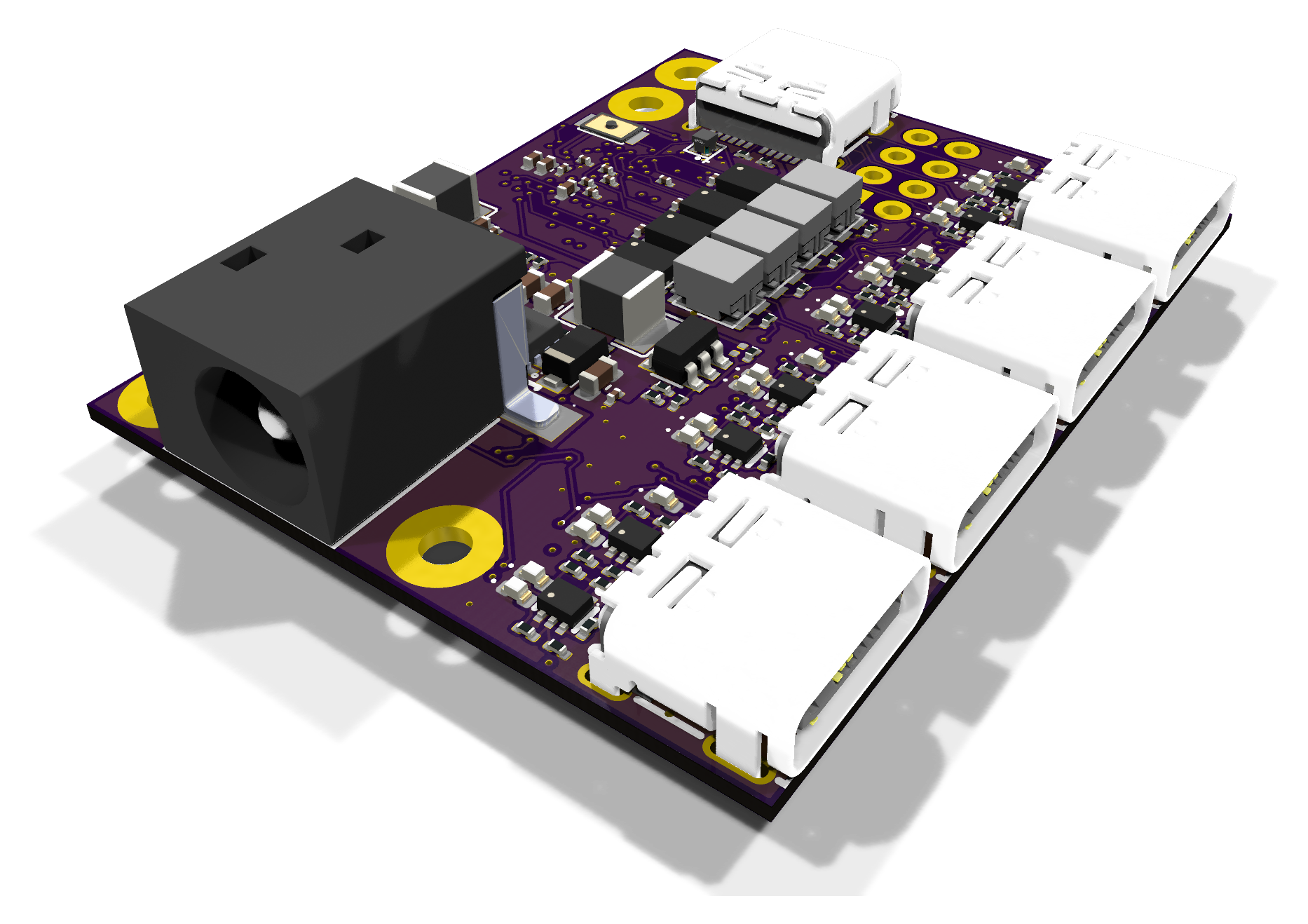
PCBGolf is a challenge from comma.ai: take their reference board, loosely based on the panda jungle, and make the assembled PCBA as small as possible while keeping every interface working and every mating connector compatible. The board must be manufacturable and assemblable at JLCPCB. The score is
bounding-box volume (mm³) + 50 × vias + 5,000 × copper layers, lowest wins.
This repo is my submitted entry, finished on the October 12, 2026 deadline. The schematic is comma's. The layout, part choices and the design changes below are mine. comma's original README is kept unchanged at the bottom.
| PCBA bounding box | 34.98 × 43.00 × 9.32 mm (includes the USB-C connector overhang) |
| Board outline | 33.9 × 42.3 mm, 0.79 mm thick |
| Copper layers | 4: signal / power / ground / signal |
| Vias | 303, all through-hole |
| Parts | 253, on both sides |
| Score (by the formula) | 14,027 + 15,150 + 20,000 = ≈ 49,200 |
The official score is assigned by comma after review.
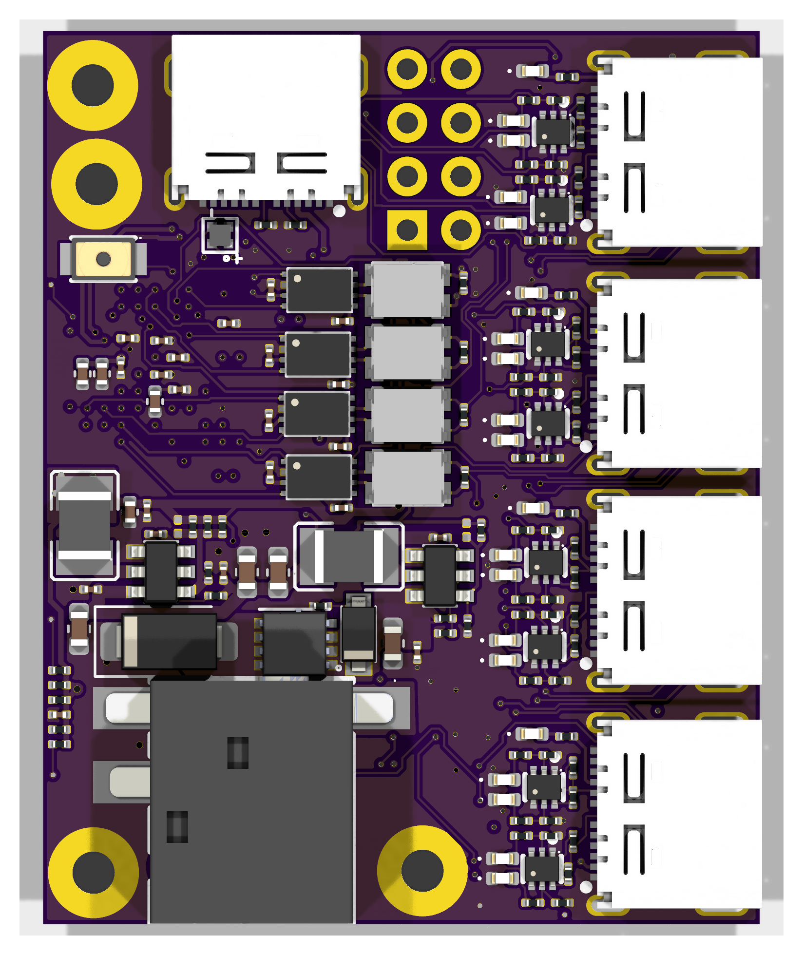 | 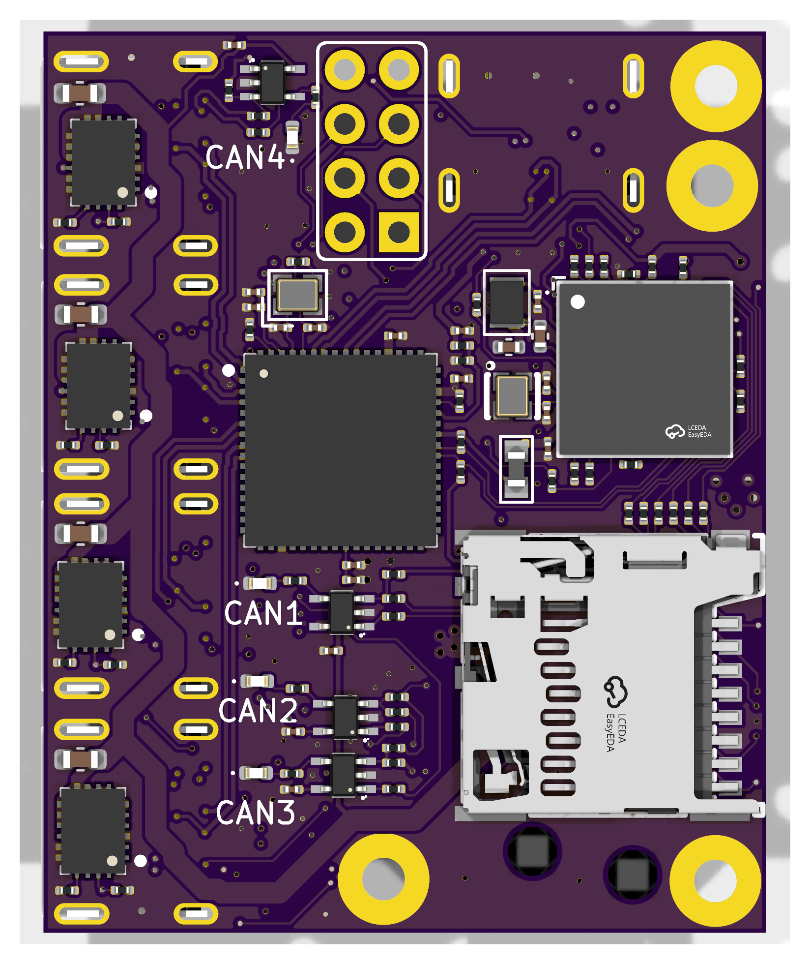 |
| Top: connectors, CAN transceivers and chokes, power supplies | Bottom: STM32 (TFBGA-100), USB hub, microSD, port eFuses |
The penalties for layers and vias outweigh size. On this board, layers (20,000) and vias (15,150) make up 71% of the score, while the volume itself is only 14,027.
The top entries went the other way: one copper layer and no vias, with a board up to twice the area. Their fixed penalty is 5,000 instead of my 35,150. Once I had committed to a 4-layer board with a BGA, no amount of shrinking could close that gap. A 4-layer board scores 30,000+ before it has any volume at all.
What I'd do differently:
The MCU is an STM32H725VGH6 (TFBGA-100), the same die as the reference STM32H725ZGT (LQFP-144). Power, USB and clock setup are unchanged.
| Signal | Reference | This board | Notes |
|---|---|---|---|
| CAN2_TX / CAN2_RX | PG9 / PG10 | PD13 / PD12 | same FDCAN3 peripheral |
| BTN (GPIO read) | PE15 | PE5 | button still also drives BOOT0 |
| CH2_SBU2 sense | PF7 | PA3 | ADC12_INP15 (was ADC3) |
| CH4_SBU2 sense | PF8 | PA2 | ADC12_INP14 (was ADC3) |
| CH2_SBU1 sense | PF9 | PC5 | ADC12_INP8 (was ADC3) |
| CH4_SBU1 sense | PF10 | PB0 | ADC12_INP9 (was ADC3) |
| CH2_IMON | PB1 | PA6 | ADC12_INP3 |
| CH3_IMON | PF11 | PA5 | ADC12_INP19 |
| CH4_IMON | PA6 | PB1 | ADC12_INP5 |
| CH4_PWR_EN | PA5 | PA7 | |
| CH1_SBU1_IGN / RELAY | PD0 / PD1 | PD6 / PD3 | |
| CH1_SBU2_IGN | PD3 | PE0 | |
| CH2_SBU1_IGN / RELAY | PD5 / PD6 | PD1 / PE1 | |
| CH2_SBU2_IGN / RELAY | PD8 / PD10 | PD0 / PD5 | |
| CH3_SBU1_IGN / RELAY | PD12 / PD11 | PD14 / PD15 | |
| CH3_SBU2_IGN / RELAY | PD9 / PD13 | PE7 / PD11 | |
| CH4_SBU1_IGN / RELAY | PD14 / PD15 | PD9 / PE8 | |
| CH4_SBU2_IGN / RELAY | PE0 / PE1 | PD8 / PD10 |
All other signals keep their reference pins.
pcbgolf.kicad_pro: KiCad 10 project (the schematics are comma's, the layout is mine)lib_jlc/, pcbgolf.pretty/: footprints, symbols and 3D models; all paths are project-relativeassets/renders/: the renders above, made with kicad-cli pcb render[blocked] Everything below is comma.ai's original challenge README, unchanged.
The schematic is loosely based on our panda jungle v2, a development and debugging board for comma devices and pandas. This version includes:
Explore in your browser with KiCanvas: PCB layout.
Schematics: Power · Microcontroller · USB & microSD · CAN · OBD-C ports

Your goal is to make the most compact, efficient board that retains the same interfaces and functionality as the original design. The lowest score wins.

Lowest score on the leaderboard by October 12, 2026 wins $1,000 cash.
Submit a .zip file containing your finalized KiCad project and a STEP file of the final assembly here.
Competitive scores will be posted on the leaderboard after review. Multiple submissions allowed.
| Qty | Value | Footprint | References |
|---|---|---|---|
| 39 | 10k | lib_jlc:R_0201_0603Metric | R1, R3, R11, R12, R28, R29, R100, R101, R102, R103, R104, R105, R122, R123, R124, R125 +23 |
| 30 | 100nF | lib_jlc:C_0201_0603Metric | C2, C4, C11, C16, C18, C22, C23, C24, C26, C27, C30, C31, C35, C36, C38, C39 +14 |
| 24 | 100 | lib_jlc:R_0201_0603Metric | R82, R83, R84, R85, R106, R107, R108, R109, R110, R111, R112, R113, R115, R117, R119, R121 +8 |
| 17 | 100k | lib_jlc:R_0201_0603Metric | R4, R5, R6, R13, R14, R15, R16, R17, R18, R19, R20, R24, R25, R52, R55, R58 +1 |
| 11 | 1k | lib_jlc:R_0201_0603Metric | R2, R21, R23, R90, R92, R94, R96, R114, R116, R118, R120 |
| 8 | LED_GREEN_0402 | lib_jlc:LED_0402_1005Metric | LED30, LED31, LED32, LED33, LED34, LED35, LED36, LED37 |
| 8 | LED_RED_0402 | lib_jlc:LED_0402_1005Metric | LED10, LED11, LED12, LED13, LED14, LED15, LED16, LED17 |
| 8 | NFET-DUAL-COMMON-SOURCE-QS5K2 | lib_jlc:SSM6N44FE-SOT563-remap | Q2, Q3, Q4, Q5, Q6, Q7, Q8, Q9 |
| 6 | 0R | lib_jlc:R_0201_0603Metric | R38, R39, R40, R41, R42, R43 |
| 5 | 10uF | lib_jlc:C_0402_1005Metric | C8, C15, C19, C20, C21 |
| 5 | 2k7 | lib_jlc:R_0201_0603Metric | R22, R62, R63, R64, R65 |
| 4 | 10u | lib_jlc:C_0201_0603Metric | C29, C33, C34, C37 |
| 4 | 10u | lib_jlc:C_0603_1608Metric | C50, C51, C52, C53 |
| 4 | 10uF | lib_jlc:C_0603_1608Metric | C1, C3, C12, C13 |
| 4 | 12pF | lib_jlc:C_0201_0603Metric | C14, C17, C28, C32 |
| 4 | 28k | lib_jlc:R_0201_0603Metric | R66, R67, R68, R69 |
| 4 | 33k | lib_jlc:R_0201_0603Metric | R70, R71, R72, R73 |
| 4 | 3k3 | lib_jlc:R_0201_0603Metric | R74, R75, R76, R77 |
| 4 | 60 | lib_jlc:R_0201_0603Metric | R46, R47, R48, R49 |
| 4 | ACT1210D_CHOKE | pcbgolf:CHOKE-3.2X2.5 | L5, L6, L7, L8 |
| 4 | CH1_PWR | lib_jlc:LED_0402_1005Metric | LED6, LED7, LED8, LED9 |
| 4 | M2_BOLT | pcbgolf:M2_BOLT | BH1, BH2, BH3, BH4 |
| 4 | MCP2542FDT-E/MNY | pcbgolf:TDFN8_2X3MC_MCH | U5, U6, U7, U8 |
| 4 | TLV9101IDCKR | lib_jlc:TLV9101-SC70-5 | U17, U18, U19, U20 |
| 4 | TPS25942 | pcbgolf:WQFN20 | U13, U14, U15, U16 |
| 4 | USB-C-FEMALEGCT | lib_jlc:USB-C-SMD_TYPE-C-USB-18 | J5, J6, J7, J8 |
| 2 | 3u3 | lib_jlc:IND_3225_3R3 | L1, L2 |
| 2 | 5.1k | lib_jlc:R_0201_0603Metric | R32, R44 |
| 2 | AP62300T | pcbgolf:SOT23-6 | U1, U2 |
| 2 | DNP | lib_jlc:C_0201_0603Metric | C6, C10 |
| 1 | 12k | lib_jlc:R_0201_0603Metric | R27 |
| 1 | 1M | lib_jlc:R_0201_0603Metric | R26 |
| 1 | 220pF | lib_jlc:C_0201_0603Metric | C25 |
| 1 | 24MHz | lib_jlc:Crystal_2016_24M | Y2 |
| 1 | 25MHz | lib_jlc:Crystal_2016_25M | Y1 |
| 1 | 2u2 | pcbgolf:0806 | L4 |
| 1 | 4.7uF | lib_jlc:C_0402_1005Metric | C54 |
| 1 | 52k3 | lib_jlc:R_0201_0603Metric | R10 |
| 1 | CAN | pcbgolf:2X04 | J4 |
| 1 | CAN0 | lib_jlc:LED_0402_1005Metric | LED2 |
| 1 | CAN1 | lib_jlc:LED_0402_1005Metric | LED3 |
| 1 | CAN2 | lib_jlc:LED_0402_1005Metric | LED4 |
| 1 | CAN3 | lib_jlc:LED_0402_1005Metric | LED5 |
| 1 | CREE-RGB-CLMVC | lib_jlc:RGB_NH-B1010 | LED1 |
| 1 | DCBARRELSMT | lib_jlc:DC-IN-SMD_DC-044D-2.5A-2.0-SMT | J1 |
| 1 | DIODEDB2W40100L | pcbgolf:SOD-123F | D2 |
| 1 | L-US-L2 | pcbgolf:0603-L | L3 |
| 1 | MICRO_SD-0472192001 | lib_jlc:microSD_Molex_5033981892 | J2 |
| 1 | SIS427-VI | pcbgolf:PP-1212-8 | Q1 |
| 1 | SPST-2-4PIN | lib_jlc:SW_TS2306A | SW1 |
| 1 | STM32H725VGH6 | lib_jlc:STM32H725-TFBGA100-remap | U3 |
| 1 | TVS-BI-DO214AA | lib_jlc:D_SMA | D1 |
| 1 | USB-C-FEMALE | lib_jlc:USB-C-J3-molex | J3 |
| 1 | USB2517 | pcbgolf:QFN64-9X9 | U4 |
It measures 33.9 × 42.3 mm and has 4 copper layers, 0.79 mm thick.
253 parts, built around the STM32H725VGH6, AP62300TWU, TPS25944ARVCR and USB2517-JZX. The full list of its parts is on this page, with links to each part's symbol and footprint where PCBKit's library has them.
From the ulyssecrn/PCBGolf repository on GitHub, at the commit this page was made from: the board is pcbgolf.kicad_pcb and its schematic pcbgolf.kicad_sch. PCBKit opens the board in the browser, with nothing to install.
Its repository states no licence, so its author keeps all rights: ask ulyssecrn before reusing the design.
chilly23/PCBGolf-master-Comma.ai
Compact PCB studies for the comma.ai PCBGolf challenge, including KiCad and EasyEDA designs, BOMs, STEP models, and routing-status reports.

YeetTheAnson/MerlynCAM
An action camera that records at 1080p@90, 1440p@60 and 4k@20 (With I2S microphone and gyro logging @ 150Hz)

gabrielpgagne/imu-geolocator-hw
An experimental project about trying to use an IMU as a geolocalization device.


OpenDrone-hw/OpenRemoteID
Open hardware concept for a standalone Remote ID module: ESP32-C3 plus GNSS receiver. Incomplete, not a compliant product.

DomPka/LuxLibre
Pick a light · Compare · Web apps · Firmware · Design your own · Build a FlashKa · Repository map · Help