4 layers100 × 100 mm
A SGSS cskpin routed
ThatguyCplus/throttleECU
STM32F411CE Throttle ECU — PID position control with AS5048A encoder, H-bridge motor, safety module
571 parts1

 ThatguyCplus/throttleECU1
STM32F411CE Throttle ECU — PID position control with AS5048A encoder, H-bridge motor, safety module
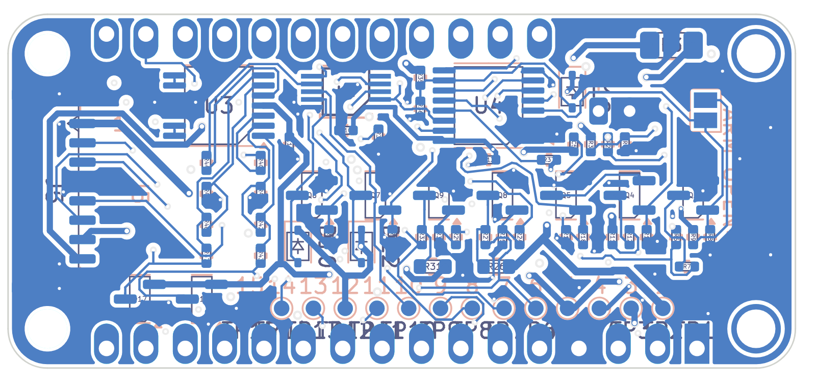
Eps tap wing is an open-source printed circuit board by ThatguyCplus, from the ThatguyCplus/throttleECU repository on GitHub. It is a 4-layer board of 50.8 × 22.9 mm with 77 parts on 58 nets, routed with 572 tracks and 69 vias.
It is built around the MCP6004-I/ST, ADS1115IDGSR and 0402B102K500NT, with the 1N4148WS and NCD0805R1 among its other parts. Its parts include 32 resistors, 19 capacitors, 6 diodes, 3 ICs and 3 connectors.


A FeatherWing for the EPS logger stack that does four jobs:
It sits between the Adalogger and the OLED FeatherWing, on stacking headers, and every cable connector is right-angle and exits a board edge. The brief is HANDOFF.md.
Status: routed and checked in KiCad 10.0.8, nothing ordered. The board is fully routed, and the Gerbers, BOM and CPL are in fab/. Read Before ordering first: several part numbers, the relay pinout and the JLC rotations still need a human check.
KiCad 10.0.8 check (with JLCPCB's rules, bench_stim_wing.kicad_dru) Result ERC 0 errors. 20 warnings: symbols drawn from KiCad 7's library differ from KiCad 10's copies, and KiCad 10 renamed G6K-2DRC 0 copper errors, 0 unconnected, 0 schematic-parity issues, including JLCPCB's 0.2 mm track-to-through-hole-pad rule and 1.0 mm / 0.15 mm text. Warnings left: stock footprint outlines touching their own pads (JLC clips those), footprints differ from KiCad 10's library copies, and J2's outline at the board edge (deliberate, edge connector)
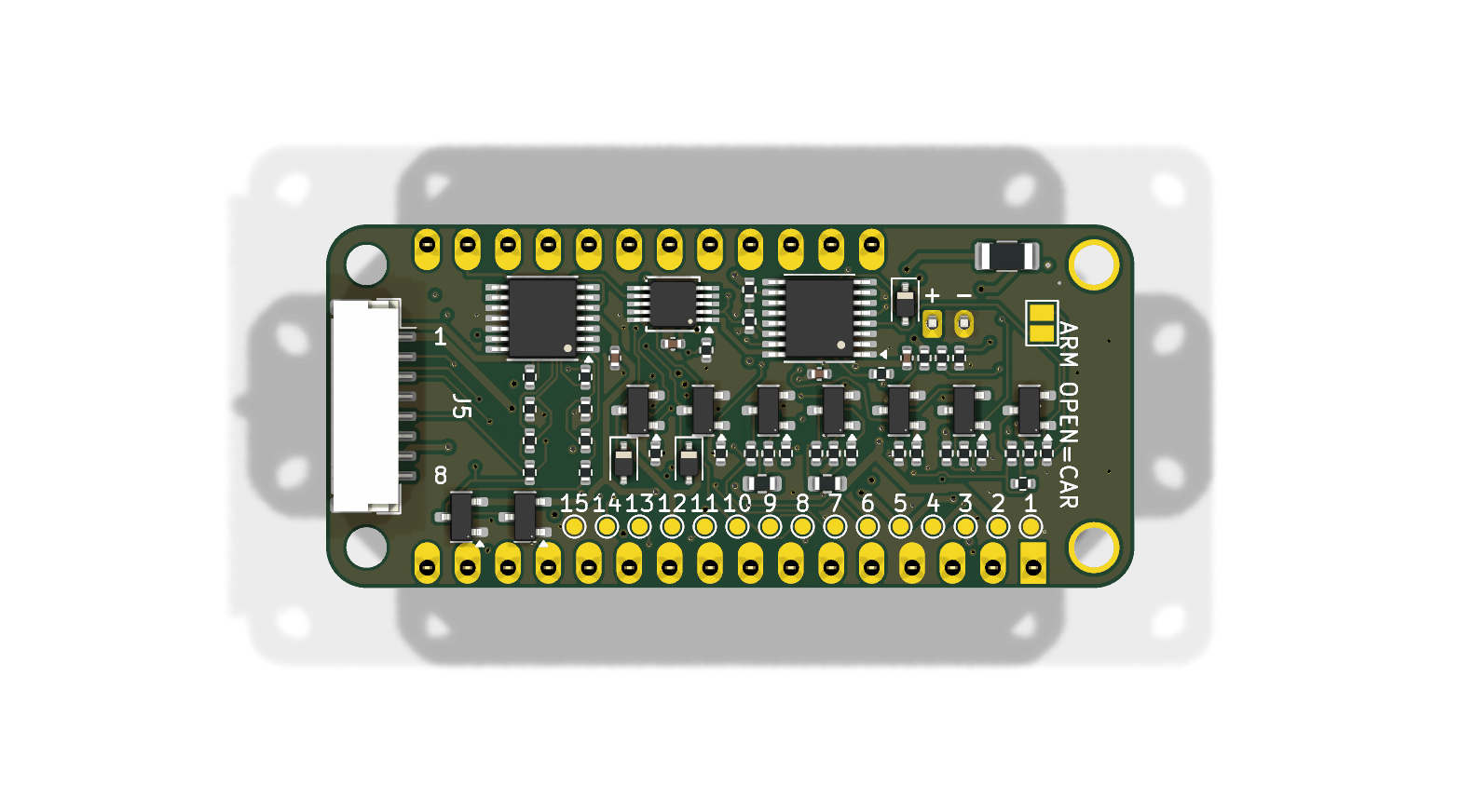
| Top (3D) | Back (3D) |
|---|---|
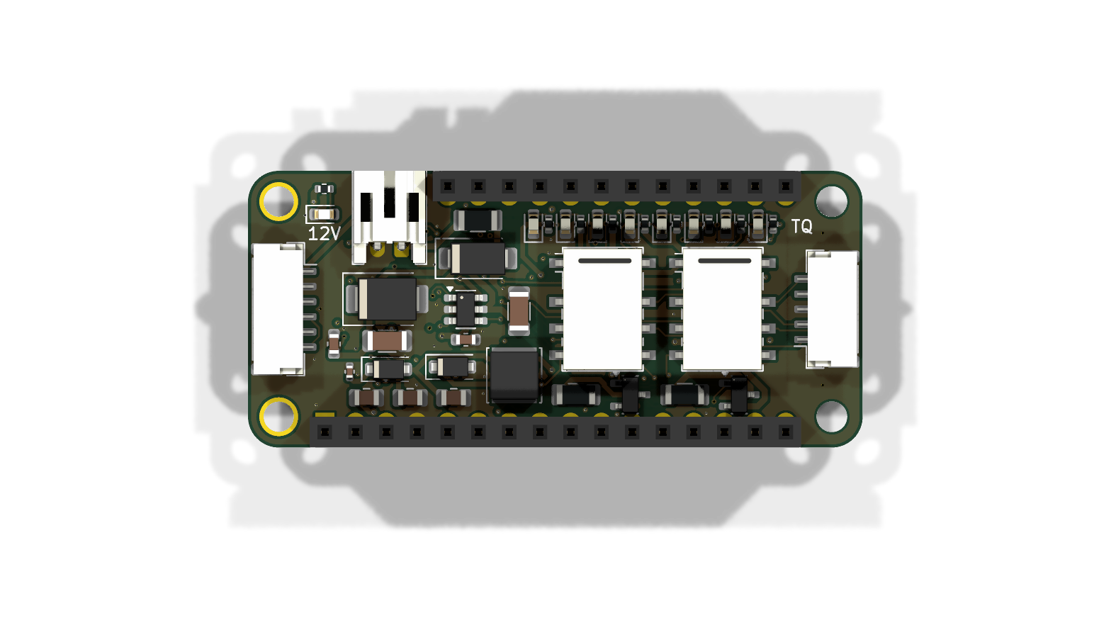 |  |
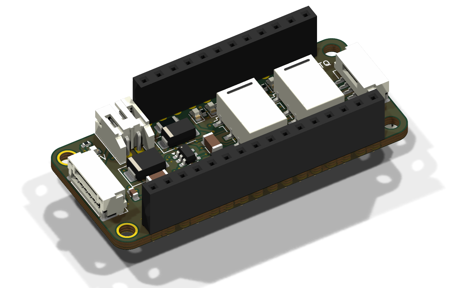
Every part has a 3D model, and the models ship with the project in bench_stim_wing.3dshapes/. They're STEP files from KiCad's official library, referenced as ${KIPRJMOD}/bench_stim_wing.3dshapes/..., so the 3D viewer and STEP export work on any machine with KiCad 7 to 10, whatever 3D libraries are installed. J1 shows the Feather stacking headers' female sockets (1×16 + 1×12). Only the test pads and the JP1 solder jumper have no model, because they're bare copper.
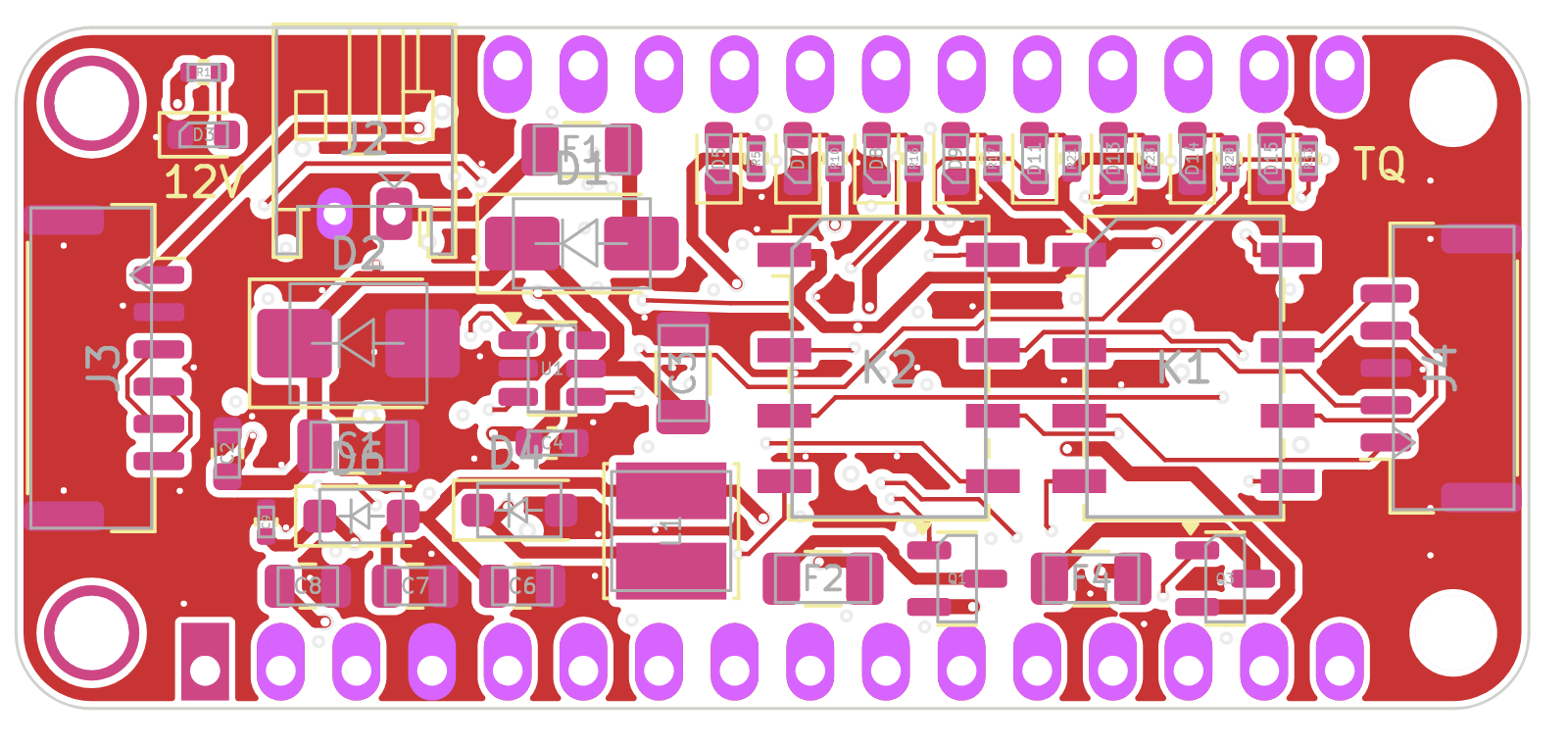
| Top layers | Back layers (seen from below) |
|---|---|
 |  |
The user asked for this to be overbuilt. Faking VT3/VT6 makes the EPS motor steer by itself: front wheels off the ground (or the rack on a bench rig), hands clear of the wheel.
| Layer | What it does |
|---|---|
| Relays, fail to the car | Every EPS line (VT3, VT6, NEP, VSP) goes through an Omron G6K relay. The NC contact connects the EPS to the car's own wire, and the NO contact connects it to this board. No power, a reset, a crash or a blown fuse all leave the EPS wired exactly as the car wires it. |
| ARM loop (hard kill) | Both relay coils and the IG1 output are powered only through the ARM loop on J5 pins 7–8. Wire a normally-closed e-stop or a key switch there. Loop open = car wiring, whatever the firmware does. The red ARM LED shows the loop is closed. |
| Enable bits | Each output also needs its own bit from the TCA9534 I2C expander. The expander powers up with every pin as an input, and 100 kΩ pull-downs hold every driver off until firmware sets the bit. |
| Clamped torque range | The DAC uses its 2.048 V internal reference and the op-amp gain is 2.2, so the torque outputs top out at 4.5 V even at full scale. They're also clamped to 0–5 V, with a 470 Ω series resistor each. |
| Inject on the EPS side only | NEP and VSP also feed the gauges, ECM, MCM, TCM and climate control. Only ever break them at the EPS with a breakout harness: the relay then isolates the EPS from the car wire, and the car side never sees the stimulus. |
Latching DTCs. The torque-sensor and sensor-supply codes (11/15/16/17/18/67) latch until erased with the SCS procedure, so a bad VT3/VT6 fake bricks assist until you clear them. The relay swaps only VT3/VT6: the real sensor stays connected to Vcc1/Vcc2 and stays powered, so the supply checks still see a real load.
Plausibility rules (from the manual, also in EPS_PINOUT.md):
Key ON, engine off: the 12 V battery isn't being charged. The DC-DC converter doesn't charge it in that state (LiBCM FAQ), so all assist current comes from the battery. Keep bench sessions short, or put a charger on the battery.
  OLED FeatherWing
  ─ female side of this wing's stacking headers ─
  BENCH STIM WING        top: relays, inductor, J2/J3/J4, LEDs   (tallest part: relays, 5.2 mm)
                         back: logic, test pads, J5              (back parts <= 1.25 mm, J5 4.25 mm)
  ─ long male tails into the Adalogger's female headers ─
  Adalogger FeatherWing  (CR1220 holder and microSD socket on its top: ~2-4 mm)
  Feather M4 CAN         (USB-C at the left end, CAN terminal block at the right end)
  EPS tap wing           (bottom wing, connectors facing down)
Why this slot:
Use Feather stacking headers (female on top, long male tails) on this wing. Check the gap with the real parts before soldering the headers.
This wing and the EPS tap wing logger run alone or together, in the car or on a bench EPS. STACK_MODES.md covers every combination: power, ground, which pins to wire, and the timers and I2C addresses they share.
The one rule: J2's ground (the stack's ground) goes to the ECU end of A4 (PG, BLK), spliced within ~10 cm of the EPS connector. On a bench, it goes to the EPS's A4 terminal. It must not go to a chassis bolt or the battery. A4 carries the 40 A motor return, so anywhere else puts an offset between the stack and the EPS's sensor ground (B9).
Leave J4.3 and J5.4 (GND) unwired in the car, so there's only one ground path. Fitted but unpowered (J2 unplugged), this board is passive: the relays rest on the car's wiring, and the logger keeps floating on its power bank.
| Spec item | This wing |
|---|---|
| 0.9" × 2.0", 0.1" holes at each corner | 22.86 × 50.8 mm, four 2.5 mm holes 2.54 mm in from the edges |
| 16-pin and 12-pin header positions | Same footprint as the EPS tap wing; make_pcb.py asserts the pad positions every build |
| Power: take 3.3 V from the Feather | The expander and DAC run on the Feather's 3V3 (about 1 mA) |
| Powering the Feather from a wing | 5 V goes into the USB pin through a Schottky (D6). On the Feather M4 CAN the USB pin is VBUS straight off the USB-C connector, and the Feather's own MBR540 then feeds its regulator, so this is the normal path (checked against Adafruit's schematic) |
| Avoid AREF, RX/TX, SPI and its CS | AREF, RX and SPI are untouched. TX is used (VSP output): only D4 and RX/TX are left free in this stack, and NEP and VSP each need their own timer |
| I2C pull-ups on Wings | Not fitted: the Adalogger already has them |
A LiPo on the Feather. If one is plugged into the Feather's JST, its charger draws up to ~200 mA from this 5 V rail. The buck is rated 0.6 A, so that still fits, but leave the LiPo off unless you want it charging.
The current clamp's supply. The HSTS016L on the tap wing takes its 5 V from the USB pin, so on 12 V alone it gets ~4.7 V. Its output is read as Vout − Vref, which cancels most of that offset, but check its zero at key-on the first time.
All connectors are right-angle and exit a board edge. JLC assembles the three GH connectors (J3, J4, J5: SMD, 1.25 mm pitch, awkward by hand). J2 (through-hole PH) and the Feather stacking headers are hand-soldered. The GH parts have locking latches: use JST GH housings (GHR-0xV-S) with SSHL-002T-P0.2 contacts, or buy pre-crimped GH leads.
J2, 12 V IN (top edge, JST PH S2B-PH-K, 2 mm). Pin 1 (marked +) is +12 V and pin 2 is GND. 2 A fuse.
J3, SAS / CAN (left end, JST GH 6-way). This is a pass-through: build one cable to the SAS, plus one pair from pins 5/6 to the Feather's CAN terminal.
| Pin | Net | Goes to |
|---|---|---|
| 1 | SAS 12V | SAS power (switched, 0.1 A PTC) |
| 2 | GND | SAS ground |
| 3 | CANH | SAS CAN-H |
| 4 | CANL | SAS CAN-L |
| 5 | CANH | Feather M4 CAN terminal pin 3 (H) |
| 6 | CANL | Feather M4 CAN terminal pin 1 (L) |
The Feather's terminal has a 120 Ω terminator behind a solder jumper (SJ2). The SAS bus here is two nodes, so close SJ2 unless the SAS end already terminates the bus.
Second microcontroller: J3 is also the stack's port for another board. Splice its CAN-H/CAN-L into the pin 5/6 lead (no ground or power wire), keep exactly two terminators on the bus (about 60 Ω across H/L, powered off), and use IDs 0x6C0–0x6CF. See AUX_LINK.md.
J4, TORQUE (right end, top, JST GH 5-way). Break the torque sensor's VT3 and VT6 wires in a breakout harness: the CAR side goes to the sensor, the EPS side to the EPS.
| Pin | Net |
|---|---|
| 1 | VT3 EPS side (gearbox 7-pin 3 / ECU B10) |
| 2 | VT3 sensor side |
| 3 | GND (leave unwired in the car: the reference comes through J2's ground, see below) |
| 4 | VT6 EPS side (gearbox 7-pin 1 / ECU B8) |
| 5 | VT6 sensor side |
J5, ECM / IG1 / ARM (right end, back, JST GH 8-way). The back silk marks "J5" with pins "1" and "8"; the pin names are below.
| Pin | Net | Notes |
|---|---|---|
| 1 | IG1 OUT | Switched 12 V, 0.5 A PTC. Bench EPS only (ECU B6) |
| 2 | NEP CAR | Car-side NEP wire (ECM) |
| 3 | NEP EPS | EPS B14 |
| 4 | GND | Separates the 12 V-level pins from the 5 V-level pins. Leave unwired in the car |
| 5 | VSP EPS | EPS B4 |
| 6 | VSP CAR | Car-side VSP wire (VSS) |
| 7 | ARM+ | 5 V out to the ARM loop (0.1 A PTC) |
| 8 | ARM | Back from the loop: powers the relay coils, enables IG1 |
Loopback for free. The tap wing's J2 reads NEP (D6), VSP (D5), VT3 (A2) and VT6 (A3). Tap the EPS side of the breakout harness and the logger records exactly what the EPS receives, including whether the relay switched.
| Block | Parts | Notes |
|---|---|---|
| 12 V input | F1 2 A fast fuse → D1 SS34 (reverse polarity) → D2 SMBJ24CA TVS → C1 10 µF/50 V | Everything on +12 V is rated ≥ 40 V; the TVS clamps a load dump to ~39 V |
| 5 V | U1 LMR16006 (40 V, 65 V transient, 0.6 A, 0.7 MHz), L1 22 µH, D4 catch diode, 56k/10k → 5.05 V | ~250 mA load: stack ~150 mA, relays 2 × 28 mA, LEDs |
| Feather feed | D6 PMEG6010 → Feather USB pin | See USB and 12 V at the same time |
| SAS power | Q1 Si2319 high side, Q2 2N7002, F2 0.1 A PTC | Expander P0. JP1 (open as shipped): bridge for "SAS always on", for use with the unmodified logger firmware |
| IG1 out | Q3 Si2319, Q4 + Q5 in series (IG1_EN and ARM), F4 0.5 A PTC | Expander P1 |
| Relays | K1 (VT3/VT6), K2 (NEP/VSP): G6K-2F-Y 5 V, Q6/Q7 drivers, 1N4148WS flyback | Expander P2, P3. Coils fed from ARM |
| NEP | D4 (PA14) → Q8 → open drain, 4.7 kΩ to 12 V, 100 Ω series | Like the ECM's open-collector output |
| VSP | TX (PB16) → Q9 → open drain, 4.7 kΩ to 5 V, 100 Ω series | Like the VSS |
| Torque | U2 MCP4728 (I2C 0x60, 2.048 V ref, gain ×1) → U3 MCP6004 on 5 V, gain 2.2 → 470 Ω → BAT54S clamp | DAC A = VT3, B = VT6. DAC C and D go straight to test pads 10/11 as spare 0–2.048 V outputs (unbuffered, ~mA); op-amp sections C/D are parked as grounded followers |
| Expander | U4 TCA9534 (I2C 0x20) | P0 SAS, P1 IG1, P2 K1, P3 K2 (outputs); P4 ARM sense, P5 12 V sense (inputs); P6/P7 on test pads |
Pulse output polarity. GPIO high pulls the output low (open drain), and the idle level is high. Both D4 and TX sit on independent timers: PA14 on TCC1/WO2 or TCC2/WO0, PB16 on TC6/WO0 or TCC0/WO4. Don't use TC3: the logger (eps_logger) uses it for its 1 kHz sample tick. The rates are low (NEP 1.5 pulses/rev: 22.5 Hz at 900 rpm; VSP ~1.24 Hz per mph, unverified), so plain micros() timing also works.
I2C addresses on the shared bus: RTC 0x68, OLED 0x3C, ADS1115 0x48, MCP4728 0x60, TCA9534 0x20. There are no clashes.
Top side, in one row above the relays. Left to right: 5V, SAS, IG1, ARM, TQ, SIG, NEP, VSP; the legend is also on the back silk. The 12 V LED is in the top-left corner. TQ and SIG light when their relay is energised. NEP and VSP blink with the pulse outputs.
The pads are numbered 1–15 on the back silk; names don't fit at JLC's 1 mm minimum text height.
| TP | Net | TP | Net | TP | Net |
|---|---|---|---|---|---|
| 1 | GND | 6 | NEP out | 11 | DAC D (raw, 0–2.048 V) |
| 2 | +12 V | 7 | VSP out | 12 | ARM |
| 3 | +5 V | 8 | VT3 out | 13 | Expander P6 |
| 4 | +3V3 | 9 | VT6 out | 14 | Expander P7 |
| 5 | USB pin | 10 | DAC C (raw, 0–2.048 V) | 15 | GND |
| Item | Value |
|---|---|
| Layers | 4: F.Cu parts + signals + GND pour, In1.Cu solid GND, In2.Cu signals + GND pour, B.Cu parts + signals + GND pour |
| Signal tracks | 0.15 mm (mA and below) |
| Power tracks | +12 V path and IG1 0.5 mm; +5 V, USB, buck SW, SAS and ARM 0.4 mm; 3V3 0.3 mm |
| Clearance | 0.127 mm; 0.21 mm from tracks to plated through-hole pads (JLCPCB's 0.2 mm pad-to-trace rule) |
| GND plane | In1 is a solid GND pour; a few low-speed signals cross it where routing needed the room |
| Silkscreen | All text >= 1.0 mm high with a 0.15 mm stroke (JLCPCB minimum) |
| JLCPCB rules | bench_stim_wing.kicad_dru, the 4-layer 1 oz set from Cimos/kicad-druid (MIT). KiCad loads it as the project's custom rules |
| Vias | 0.45/0.2 mm signal, 0.6/0.3 mm power |
| Assembly | Both sides (SMD top and back). The back carries only parts ≤ 1.25 mm tall |
| File | What it is |
|---|---|
| bench_stim_wing.kicad_sch / schematic PDF | Schematic (generated) |
| bench_stim_wing.kicad_pcb | Board, 50.8 × 22.86 mm (FeatherWing), 4 layers |
| doc/ | 3D renders (KiCad 10) and layer renders of the top and back |
| bench_stim_wing.3dshapes/ | The 3D models every footprint points to (KiCad library STEP files, CC-BY-SA 4.0 with the KiCad library exception) |
| fab/ | Gerbers + drill (zipped), JLC BOM and CPL. All SMD parts including the GH connectors; J1 (stacking headers), J2, JP1 and the test pads are excluded |
| gen/ | Generators. Everything comes from gen/design.py (parts and nets) and gen/placement.py (positions, silk, hand stubs). gen/bench_stim_wing.ses is the accepted Freerouting result |
The board was generated in a Linux cloud session. The generators ran on KiCad 7.0.11, the version Ubuntu ships. Sign-off ran on KiCad 10.0.8, which gen/setup_kicad10.sh installs from the official kicad/kicad Docker image. That image comes through Google's Docker Hub mirror, because KiCad's Launchpad PPA is blocked there and Docker Hub rate-limits anonymous pulls. The script runs KiCad 10 through chroot, which needs root. Routing used Freerouting 1.9.0 on Java 21, under xvfb-run. The files are written in KiCad 7's format. KiCad 10 opens them and asks to upgrade on save. Upgrading is fine, but then the generators would overwrite your edits, so pick one way of working.
cd gen
sh route.sh --keep-routing   # rebuild everything from the committed routing (bench_stim_wing.ses)
sh route.sh                  # full re-route with Freerouting (a different result every run)
route.sh expects kicad-cli and a Python that can import pcbnew (PY=...). A full re-route also needs the Freerouting 1.9 jar (JAR=...). On Windows with KiCad 10, point PY at KiCad's bundled python.exe, and set KICAD_SYMBOL_DIR / KICAD_FOOTPRINT_DIR if the libraries aren't found.
How it got to 0 unconnected (and JLCPCB-clean):
-oit 100. Without that flag the post-route optimiser runs for hours.make_pcb.py grows the through-hole pads in the router's copy of the board instead (dsn_router_tweaks).MANUAL_ROUTES, which belongs to the committed bench_stim_wing.ses). KiCad 7 exports some back-side pads to Freerouting on the wrong layer, which leaves a few connections "connected" in its eyes but open on the board. maze_route.py (a small 4-layer grid router that keeps every clearance) and find_via.py close them:
check_netlist.py checks every pin in the exported netlist against design.py. When kicad10-cli is installed, route.sh also runs KiCad 10's ERC, its DRC with schematic parity, and the 3D renders.
How the CPL is made (gen/export_fab.py), the same way Bouni's kicad-jlcpcb-tools plugin does it:
cpl_rotations_db.csv):| Footprint | Correction |
|---|---|
| SOT-23, SOT-23-6 | −90° |
| TSSOP-14/16, MSOP-10 | 270° (MSOP-10 isn't listed; it's the same package as VSSOP-10) |
| Omron G6K-2F-Y relay | 270° |
| JST GH (and PH) | 180° |
Other tools: the schematic symbols carry MPN and LCSC fields, which is what the kicad-jlcpcb-tools plugin and JLC's own KiCad workflow read. Opening the project with that plugin should therefore pick up every part number. All footprints and symbols use KiCad's standard library names (Resistor_SMD:R_0402_1005Metric and so on), plus the project's own bench_stim_wing libraries for the Feather headers and JP1, through ${KIPRJMOD} library tables.
All 38 line items have LCSC numbers in fab/bench_stim_wing_bom_jlc.csv.
| Part | LCSC | Notes |
|---|---|---|
| LMR16006YQDDCRQ1 buck | C544521 | Extended. TI rates it 40 V, 65 V transient. The TVS clamps at ~39 V |
| MCP4728-E/UN DAC | C108207 | Extended |
| MCP6004T-I/ST op-amp | C50282 | Extended. Microchip, tape & reel. Replaced C185811 (tube version: only 3 in stock at JLC). Fallback: UMW MCP6004T-I/ST, C32713110 |
| TCA9534PWR expander | C783615 | Extended |
| Si2319CDS-T1-GE3 P-FET | C146287 | Vishay. Avoid the "-JSM" copy, C18191323, which has a different rating |
| G6K-2F-Y DC5 relay | C231389 | In stock. C1560486 is the same MPN but listed unavailable |
| SWPA4030S220MT 22 µH | C83472 | Isat 1.3 A |
| SMBJ24CA TVS | C1973089 | Bourns. Every SMBJ24CA listing found is Extended |
| PMEG6010CEH-QX Schottky | C5311567 | Extended. AEC-Q101 version of PMEG6010CEH, same SOD-123F part. Replaced C110797 (no stock at JLC) |
| SS34 Schottky | C8678 | Basic, but marked "not recommended for new designs"; alternative is FOSAN C5119706 |
| BAT54S | C171786 | |
| JST GH headers, SM05B / SM06B / SM08B-GHS-TB(LF)(SN) | C189896 / C133065 / C265111 | Extended. J4 / J3 / J5. C133065 showed 0 stock on one LCSC page |
| 2 A fuse, 1206 | C3105 | Littelfuse 0466002.NRHF, the halogen-free version of 0466002.NR |
| 0.1 A PTC, 60 V | C2153714 | Littelfuse 1206L010/60WR |
| 0.5 A PTC, 30 V | C7542947 | LUTE 1206L050/30NR. No LCSC listing found for the Littelfuse 1206L050/30WR |
| 10 µF 50 V 1206 | C13585 | |
| 4.7 µF 50 V 1206 | C51205 | |
| 10 µF 25 V 0805 | C15850 | Basic |
| 100 nF 50 V 0603 | C14663 | Basic. Showed out of stock on one LCSC page |
| 0402 resistors (100R, 470R, 1k, 10k, 12k, 22k, 33k, 100k) | C25076, C25117, C11702, C25744, C25752, C25768, C25779, C25741 | UNI-ROYAL, Basic |
| 56k 0402 | C25796 | UNI-ROYAL. Extended, not Basic |
| 4.7k 0603 | C23162 | Basic |
| 2N7002 | C8545 | Basic |
| 1N4148WS | C2128 | Basic |
| LEDs 0603, Hubei KENTO: red KT-0603R, yellow KT-0603Y, blue KT-0603B, green KT-0603G | C2286, C2287, C2288, C12624 | Red is Basic; the others are Extended. Replaced the Everlight C72038/C72041/C72043, which JLC had no stock of |
About 19 Extended part types, at about $3 each in setup fees. Swapping R3 56k for a Basic value would mean recomputing the 5 V divider. Not worth it.
Nothing is written yet. A bench sketch (or a bench mode in eps_logger) needs:
eps_logger/config.h says D4 is the CAN boost enable. Adafruit's Feather M4 CAN schematic shows boost enable and CAN standby are internal pins PB13 and PB12, and D4 (PA14) only goes to the header. Fix that comment when the firmware is touched.
| Qty | Value | Footprint | References |
|---|---|---|---|
| 14 | BYPASS | eps_tap_wing:SolderJumper_Bypass | JP1, JP2, JP3, JP4, JP5, JP6, JP7, JP8, JP9, JP10, JP11, JP12, JP13, JP14 |
| 13 | 1nF | Capacitor_SMD:C_0402_1005Metric | C1, C2, C3, C4, C8, C9, C10, C11, C12, C14, C15, C16, C17 |
| 11 | 100k | Resistor_SMD:R_0402_1005Metric | R8, R12, R13, R14, R16, R18, R20, R25, R27, R29, R31 |
| 11 | 1M | Resistor_SMD:R_0402_1005Metric | R1, R2, R3, R4, R5, R6, R7, R24, R26, R28, R30 |
| 6 | 100nF | Capacitor_SMD:C_0402_1005Metric | C5, C6, C7, C13, C18, C19 |
| 5 | 1N4148WS | Diode_SMD:D_SOD-323 | D1, D2, D3, D4, D5 |
| 4 | 33k | Resistor_SMD:R_0402_1005Metric | R15, R17, R19, R21 |
| 2 | 10k | Resistor_SMD:R_0402_1005Metric | R9, R22 |
| 2 | 47k | Resistor_SMD:R_0402_1005Metric | R10, R23 |
| 2 | MCP6004 | Package_SO:TSSOP-14_4.4x5mm_P0.65mm | U1, U2 |
| 1 | 100R | Resistor_SMD:R_0402_1005Metric | R11 |
| 1 | 1k | Resistor_SMD:R_0805_2012Metric_Pad1.20x1.40mm_HandSolder | R32 |
| 1 | ADS1115 | Package_SO:TSSOP-10_3x3mm_P0.5mm | U3 |
| 1 | Current clamp | TerminalBlock_Phoenix:TerminalBlock_Phoenix_MPT-0,5-4-2.54_1x04_P2.54mm_Horizontal | J3 |
| 1 | EPS taps | Connector_JST:JST_XA_B15B-XASK-1_1x15_P2.50mm_Vertical | J2 |
| 1 | Feather M4 CAN | eps_tap_wing:Feather_Wing_Headers | J1 |
| 1 | RED | LED_SMD:LED_0805_2012Metric_Pad1.15x1.40mm_HandSolder | D6 |
ThatguyCplus/throttleECU
STM32F411CE Throttle ECU — PID position control with AS5048A encoder, H-bridge motor, safety module

ThatguyCplus/throttleECU
STM32F411CE Throttle ECU — PID position control with AS5048A encoder, H-bridge motor, safety module

ThatguyCplus/throttleECU
STM32F411CE Throttle ECU — PID position control with AS5048A encoder, H-bridge motor, safety module

Twisted-Fields/acorn-robot-electronics
PCB hardware designs in KICAD for Acorn, the precision farming rover from Twisted Fields.


gallicchio/AMOD-and-RFMOD
The tutorial's 2x12 adapter (/mudd/133electronics/icepi-zero-dac-adc/adapterboard/) with a 2 x 6 right-angle Pmod socket on a 15 mm extension of its right-hand end, so an Icepi Zero can drive AMOD-A's and RF-MOD's Pmod…

P-Shreyas543/BatteryPack_16S_A4_Breakout
KiCad 10 project for a 14S (58.8 V max, 50.4 V nominal) 18650 battery pack on a 297 × 210 mm (A4) 4-layer PCB, built as a BMS breakout and training board.


Celnardur/rfc_tackle_sensor
Open a git bash terminal in the directory of your choosing and call the following command:

elagil/net-bmp
An Ethernet-connected SWD/JTAG debug adapter (blackmagic probe)
It measures 50.8 × 22.9 mm and has 4 copper layers, 1.6 mm thick.
77 parts, built around the MCP6004-I/ST, ADS1115IDGSR, 0402B102K500NT and 1N4148WS. The full list of its parts is on this page, with links to each part's symbol and footprint where PCBKit's library has them.
From the ThatguyCplus/throttleECU repository on GitHub, at the commit this page was made from: the board is steering_control_unit/data_capture/hardware/eps_tap_wing/eps_tap_wing.kicad_pcb and its schematic f411testingreliablitymotor/c2000_f280049_throttle/throttleecupcb/TasaruV0.0.1/TasaruV0.0.1.kicad_sch. PCBKit opens the board in the browser, with nothing to install.
Its repository states no licence, so its author keeps all rights: ask ThatguyCplus before reusing the design.