
4 layers60 × 100 mm

A small 2.4GHz module based on the nRF24L01P+, with an SMA jack for an external antenna, an on-board RFX2401C PA/LNA for extra range, and a breadboard friendly SPI header. Runs from 3.3V or 5V off an on-board LDO.
NRF24 is an open-source printed circuit board by sneakylizard123-4, from the sneakylizard123-4/nRF24 repository on GitHub, published under the CERN-OHL-P-2.0 licence. It is a 4-layer board of 50 × 30 mm with 40 parts on 25 nets, routed with 128 tracks and 221 vias.
It is built around the RFX2401C, NRF24L01P-R and TLV75733PDBV. Its parts include 22 capacitors, 5 resistors, 5 inductors, 3 ICs and 2 connectors.


A small 2.4GHz module based on the nRF24L01P+, with an SMA jack for an external antenna, an on-board RFX2401C PA/LNA for extra range, and a breadboard friendly SPI header. Runs from 3.3V or 5V off an on-board LDO.
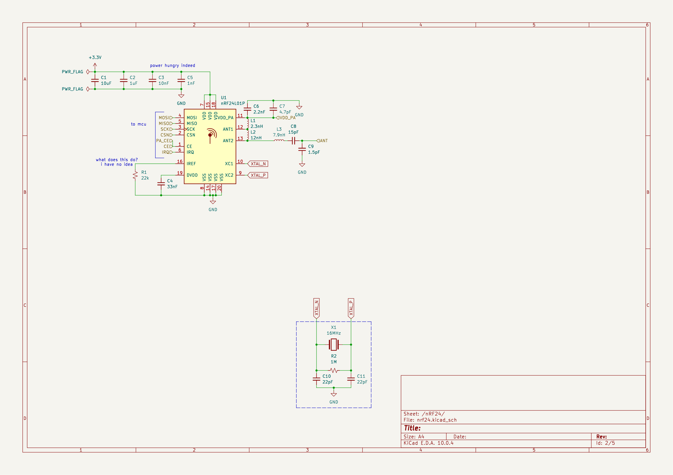
The 16MHz crystal clocks the radio, a 1M bias resistor plus 22pF load caps set the oscillator frequency.
graph LR
  VIN[VIN: header pin 2, 3.3V or 5V]
  VIN --> LDO[U2 TLV75733]
  LDO --> R[+3.3V rail]
  R --> R1[U1 nRF24L01P+]
  R --> R2[U3 RFX2401C PA/LNA]
  R1 -->|ANT1/ANT2| Balun[LC balun + harmonic filter]
  Balun --> R2
  R2 --> Match[LC match + DC block]
Match --> SMA[J2 antenna port]50.0 x 30.0 mm, 4-layer, 1.6mm thick, 5mm radius corners, on the JLCPCB JLC04161H-7628 stackup. F.Cu carries the routing, In1.Cu is a solid ground plane, In2.Cu is the +3.3V plane, and B.Cu has the leftover CE and VIN runs.
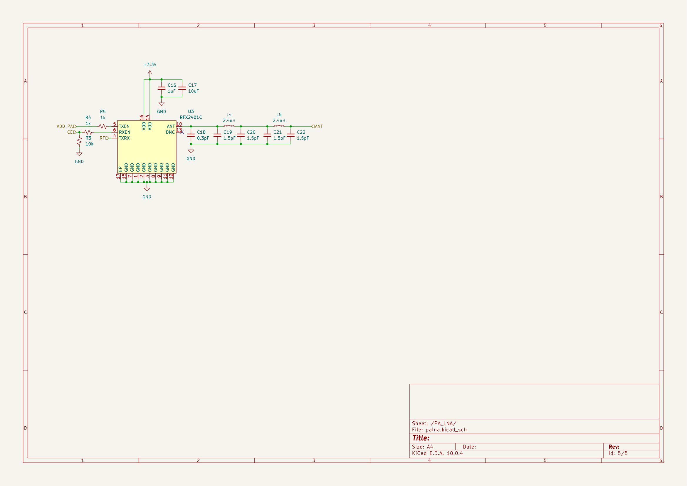
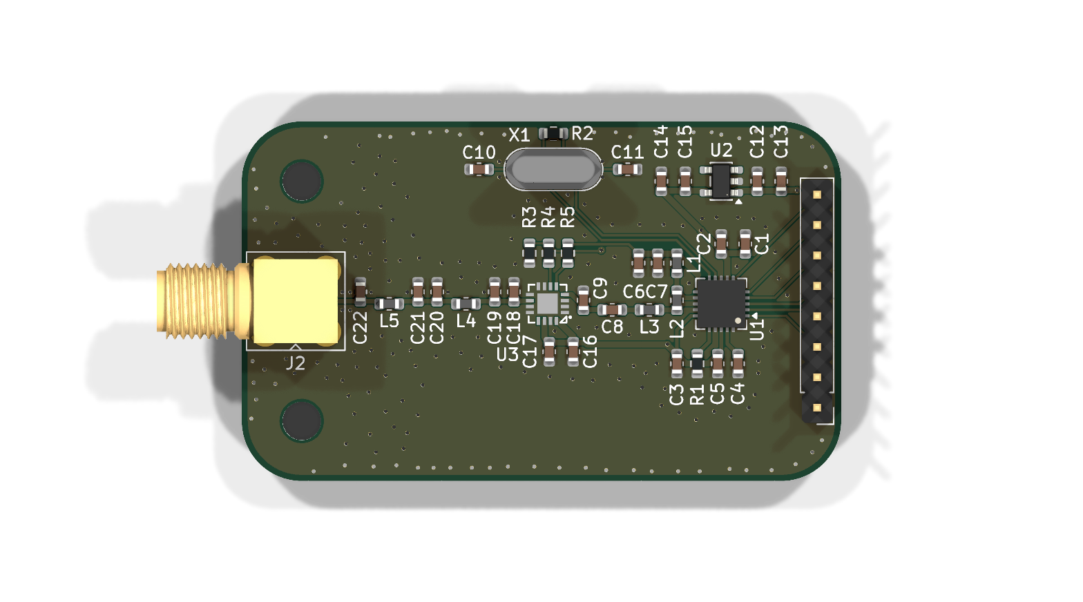
The PA/LNA sits on the RF line between the radio and the SMA, which hangs off the board edge.
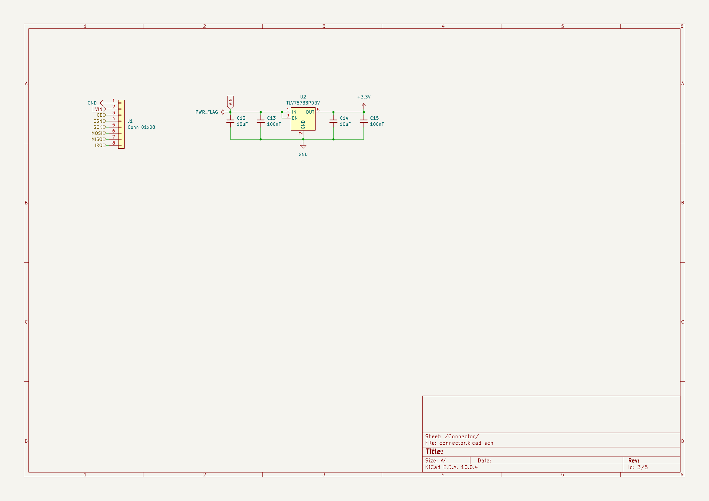
| Pin | Function |
|---|---|
| 1 | GND |
| 2 | VIN (3.3-5V) |
| 3 | CE |
| 4 | CSN |
| 5 | SCK |
| 6 | MOSI |
| 7 | MISO |
| 8 | IRQ |
| Item | Cost |
|---|---|
| Components (per board) | $6.55 |
| Components (first order, MOQ rounded, 5 boards) | $20.12 |
| PCB (qty 5, 4-layer) | $8.10 ($1.62/board) |
| Controlled impedance (optional) | not quoted |
| Total (5 boards, parts + boards) | $28.22 |
| Shipping (economy direct line, 8-13 business days) | $8.47 |
Quoted 2026-09-29 from the JLCPCB instant quote on the uploaded gerbers. The detected board is 4 layer 30x50mm, qty 5. The $8.10 is a web-tier price made up of a $8.00 promo plus $0.10 edge rounding; the JLCONE desktop tier came out at $2.10 for the same order. Shipping, tax, rush and controlled impedance are all outside that number. Confirm the total at checkout, the promo may not persist.
See BOM.csv for the full part list with LCSC part numbers, prices and supplier links.
Not built yet. Board house is JLCPCB, 4-layer FR4 on the JLC04161H-7628 stackup, 1.6mm, HASL (lead-free), green, 50.0 x 30.0 mm inside a 100x100mm panel, qty 5. That stackup puts 0.2104mm of prepreg between F.Cu and In1.Cu, so the antenna trace on F.Cu references a ground plane 0.2104mm away, and In2.Cu carries the +3.3V plane.
The board is hand-routed, no autorouter. The antenna-side net (U3-ANT) runs
as single-ended 0.4mm microstrip on F.Cu from the RFX2401C antenna pin to J2,
with the matching network (C19, L4, C20, C21, L5, C22) as an alternating LC
ladder along the way. The nRF24 differential PA outputs (U1-ANT1, U1-ANT2)
are also 0.4mm and stay paired until the balun. 221 through vias, mostly
stitching the top layer down to the In1.Cu ground plane.
The 0.4mm width is close but not exact. Over 0.2104mm of prepreg, 0.4mm works out to 54 ohm and 0.46mm works out to 50, which stays inside the 45-55 ohm band that JLCPCB's published +/-10% impedance tolerance allows on 4 layer and up. The 0.06mm change has not been made yet. See Known Issues.
|-- kicad/            # PCB source files (.kicad_sch / .kicad_pcb)
|   |-- parts/        # Project-local symbol / footprint / 3D libs
|   `-- production/   # Gerbers, drill files, netlist, position files
|-- images/           # Schematic exports and renders
|   |-- schematic/    # Per-sheet PNGs
|   |-- pcb/          # Layout progress shots
|   `-- screenshots/  # Build photos
|-- BOM.csv           # Bill of materials w/ links + total cost line
|-- JOURNAL.md        # Work journal
|-- LICENSE           # CERN OHL v2-P (hardware)
`-- LICENSE-MIT # MIT (code)Hardware (schematics, PCB layout, CAD and 3D models) is under CERN OHL v2-P, the permissive variant, because this is a personal build and not a product. If boards are ever sold, relicense to CERN-OHL-S.
SPDX-License-Identifier: CERN-OHL-P-2.0Any code in this repository (build scripts, and any firmware added later) is licensed under the MIT License.
SPDX-License-Identifier: MIT| Qty | Value | Footprint | References |
|---|---|---|---|
| 5 | 1.5pF | Capacitor_SMD:C_0603_1608Metric | C9, C19, C20, C21, C22 |
| 4 | 10uF | Capacitor_SMD:C_0603_1608Metric | C1, C12, C14, C17 |
| 2 | 100nF | Capacitor_SMD:C_0603_1608Metric | C13, C15 |
| 2 | 1k | Resistor_SMD:R_0603_1608Metric | R4, R5 |
| 2 | 1uF | Capacitor_SMD:C_0603_1608Metric | C2, C16 |
| 2 | 2.4nH | Inductor_SMD:L_0603_1608Metric | L4, L5 |
| 2 | 22pF | Capacitor_SMD:C_0603_1608Metric | C10, C11 |
| 2 | MountingHole | MountingHole:MountingHole_3.2mm_M3 | H1, H2 |
| 1 | 0.3pF | Capacitor_SMD:C_0603_1608Metric | C18 |
| 1 | 10k | Resistor_SMD:R_0603_1608Metric | R3 |
| 1 | 10nF | Capacitor_SMD:C_0603_1608Metric | C3 |
| 1 | 12nH | Inductor_SMD:L_0603_1608Metric | L2 |
| 1 | 15pF | Capacitor_SMD:C_0603_1608Metric | C8 |
| 1 | 16MHz | Crystal:Crystal_SMD_3225-4Pin_3.2x2.5mm | X1 |
| 1 | 1M | Resistor_SMD:R_0603_1608Metric | R2 |
| 1 | 1nF | Capacitor_SMD:C_0603_1608Metric | C5 |
| 1 | 2.2nF | Capacitor_SMD:C_0603_1608Metric | C6 |
| 1 | 2.3nH | Inductor_SMD:L_0402_1005Metric | L1 |
| 1 | 22k | Resistor_SMD:R_0603_1608Metric | R1 |
| 1 | 33nF | Capacitor_SMD:C_0603_1608Metric | C4 |
| 1 | 4.7pF | Capacitor_SMD:C_0603_1608Metric | C7 |
| 1 | 7.9nH | Inductor_SMD:L_0402_1005Metric | L3 |
| 1 | Conn_01x08 | Connector_PinHeader_2.54mm:PinHeader_1x08_P2.54mm_Vertical | J1 |
| 1 | Conn_Coaxial | Connector_Coaxial:SMA_Amphenol_901-143_Horizontal | J2 |
| 1 | RFX2401C | RFX2401C:QFN-16_L3.0-W3.0-P0.50-BL-EP1.7 | U3 |
| 1 | TLV75733PDBV | Package_TO_SOT_SMD:SOT-23-5 | U2 |
| 1 | nRF24L01P | Package_DFN_QFN:QFN-20-1EP_4x4mm_P0.5mm_EP2.5x2.5mm | U1 |

bemelab/nrf24L01-modules
nRF24L01+ tabanlı RF modül tasarımları. Her proje kendi klasöründe, kendi README'si ve tasarım notlarıyla durur.


Madjogger1202/RP2350B-Flight-controller
Ultra-compact flight controller for mini quadcopters, based on RP2350B MCU.

OpenDrone-hw/OpenRX
OpenRX open-source ExpressLRS receiver family hub; board sources live in four dedicated hardware repositories.

AnyLeaf/elrs-hardware
This repo contains open source hardware information for AnyLeaf ELRS receivers

OpenDrone-hw/OpenRX-Gemini
Open-source dual-radio, dual-band ExpressLRS receiver for Gemini and Xrossband.

Paschalis/UAV-TelemetryLink
Receiver and transmitter solution for GCS using ELRS, mLRS, and MAVLink for reliable telemetry and control.
It measures 50 × 30 mm and has 4 copper layers, 1.61 mm thick.
40 parts, built around the RFX2401C, NRF24L01P-R and TLV75733PDBV. The full list of its parts is on this page, with links to each part's symbol and footprint where PCBKit's library has them.
From the sneakylizard123-4/nRF24 repository on GitHub, at the commit this page was made from: the board is kicad/nRF24.kicad_pcb and its schematic kicad/connector.kicad_sch. PCBKit opens the board in the browser, with nothing to install.
Its repository publishes it under the CERN-OHL-P-2.0 licence: you may reuse it on that licence's terms (keep the author's notice, and for a copyleft licence share your changes alike).