2 layers99.9 × 99.9 mm

 skiselev/minimax808560
Simple Intel 8085 based Single Board Computer (SBC)
Mini8085 is an open-source printed circuit board by skiselev, from the skiselev/minimax8085 repository on GitHub, published under the GPL-3.0 licence. It is a 2-layer board of 100 × 80 mm with 45 parts on 87 nets, routed with 1,285 tracks and 62 vias.
It is built around the MAX232ACSE+, 27C128-15 and 74HC573. Its parts include 15 capacitors, 8 ICs, 5 connectors, 3 resistors and 2 diodes. It belongs with the computers and single-board computers boards and the FPGA and CPLD boards of this library.


Minimal 8085 Single Board Computer
The MiniMax8085 project has been brewing for almost three years. In the spring of 2014 my kids and I visited a local surplus store, where my kids found some Intel 8000 series parts in the kids-fill-your-bucket area. Among these ICs were there: an 8085 CPU, an 8155 RAM with I/O ports and timer, a couple of 8255 PPIs, an 8282 latch, and some 27C128 UV EPROMs. It looked like a good start for an 8085 based computer that can be used to teach my kids some computer design and programming basics. I wanted the project to be simple to build, with a minimal number of components, but yet to be a fully functional single board computer (e.g. to include the memory and an input/output device, for example a UART) with an extension bus. I checked the Internet for existing homebrew 8085 computers and found Roman Fülek's NCB85 and NCB85v2 projects, and Glitch Works 8085 projects. While I liked these projects, they didn't quite meet my project design goals:
The resulting design includes 8085 CPU, 8251 USART, 32 KiB SRAM, 32 KiB or 16 KiB ROM. It uses a GAL16V8/ATF16V8 simple programmable logic device (SPLD) instead of discrete logic ICs for the address decode and the frequency divider for USART. It reduces the number of components, allows for tweaking the configuration by re-programming the SPLD, and provides an introduction to the programmable logic devices.
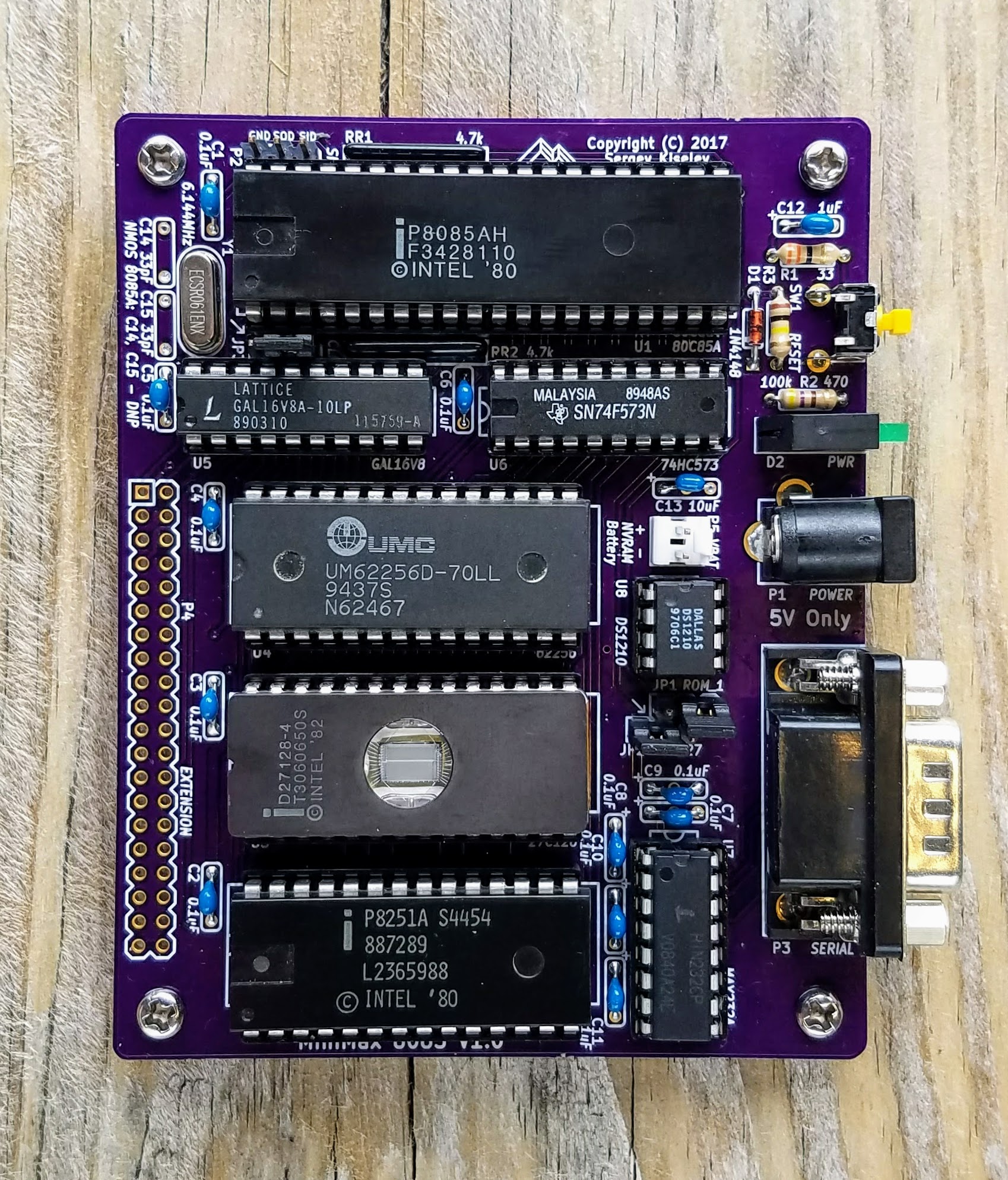
The MiniMax8085 is based on the Intel 8085A CPU (U1). The 74*573 octal latch (U6) is used to demultiplex the lower 8-bit of address and data bus. The board uses the Intel 8251A USART (U2) for serial input / output, for example for connecting a console. The MAX232A RS-232 driver/receiver (U7) is used to convert TTL logic levels to RS-232 voltage. The 62256 32 KiB SRAM (U4) is used for the system RAM. The RAM is battery backed using the DS1210 NVRAM controller (U8). The board supports a variety of ROM options (U3): The 28C256 EEPROM; UV EPROMs, such as 27C256 (32 KiB), 27C128 (16 KiB), and 27C64 (8 KiB); or The 29C256 Flash ROM ICs. Normally the ROM is mapped to the CPU memory beginning from the address 0x0000, while the RAM is mapped beginning from the address 0x8000. The ROM and RAM addresses can be swapped by pulling /SWAP_MEM signal low. This can be used, for example, to implement a CP/M extension card. The GAL16V8 simple programmable logic device (U5) implements all the required "glue" logic functions:
Please refer to the Simple Programmable Logic Device section below for more details regarding the SPLD configuration and programming.
The MiniMax8085 includes a 40-pin extension connector (P4), that features the 8085A address and data buses, and control signals. Please refer to the Jumpers and Connectors section below for the connector pinout and signals description.
These jumpers configure how pins 1 and 27 of the ROM IC (U3) are connected. The jumper settings are printed on the bottom side of the PCB.
| ROM Type | Jumper JP1 Position - ROM Pin 1 Connection | JP2 Position - ROM Pin 27 Connection |
|---|---|---|
| 27C128, 27C64, 27128, 2764 | 2-3 - pin 1 connected to VCC | 1-2 - pin 27 connected to VCC |
| 27C256 | 2-3 - pin 1 connected to VCC | 2-JP1 pin 1 (jumper installed vertically), pin 27 connected to A14 |
| 28C256 | 1-2 - pin 1 connected to A14 | 2-3 - pin 27 connected to /WR |
| 29C256 | 2-JP2 pin 3 (jumper installed vertically), pin 1 connected to /WR | 2-JP1 pin 1 (jumper installed vertically), pin 27 connected to A14 |
JP3 sets the USART input clock frequency
| Jumper Position | Crystal Y1 Frequency (CPU Frequency) | USART Clock Frequency | USART Bit rate |
|---|---|---|---|
| 1-2 | 6.144 MHz (3.073 MHz), 8 MHz (4 MHz), 9.8304 MHz (4.9152 MHz) | 307.2 kHz | 19200 bps (default) or 2400 bps, depending on USART configuration |
| 1-2 | 12.288 MHz (6.144 MHz), 16 Mhz (8 MHz) | 614.4 kHz | 38400 bps (default) or 4800 bps, depending on USART configuration |
| 2-3 | 6.144 MHz (3.073 MHz), 8 MHz (4 MHz), 9.8304 MHz (4.9152 MHz) | 153.6 kHz | 9600 bps (default) or 1200 bps, depending on USART configuration |
| 2-3 | 12.288 MHz (6.144 MHz), 16 MHz (8 MHz) | 307.2 kHz | 19200 bps (default) or 2400 bps, depending on USART configuration |
Connect regulated +5V power supply to this connector.
| Pin | Description |
|---|---|
| tip (the inner contact) | Positive terminal - +5V |
| barrel / sleeve | Negative terminal - ground |
Connector P2 contains the 8085A CPU serial input and output lines.
| Pin | Description |
|---|---|
| 1 | Ground |
| 2 | SOD / Serial Output Data |
| 3 | SID / Serial Input Data |
P3 is the serial port connector. It is normally used for connecting a console or terminal. P3 uses pinout similar to that of IBM AT serial port (with some signals missing). Use a null modem cable to connect to a PC.
| Pin Number | Signal Name | Description and Notes |
|---|---|---|
| 1 | DCD | Carrier Detect; Not used - Not connected on the SBC |
| 2 | RX | Receive Data; Input to SBC |
| 3 | TX | Transmit Data; Output from SBC |
| 4 | DTR | Data Terminal Ready; Not used - Not connected on the SBC |
| 5 | Signal Ground | Connected to the SBC GND signal |
| 6 | DSR | Data Set Ready; Not used - Not connected on the SBC |
| 7 | RTS | Request to Send; Output from SBC |
| 8 | CTS | Clear to Send; Input to SBC |
| 9 | RI | Ring Indicator; Not used - Not connected on the SBC |
| Shield | DE9 Shield | Connected to the SBC GND signal |
Connector P4 contains the 8085A CPU address and data buses, and control signals.
| Pin | Signal | Description | Pin | Signal | Description |
|---|---|---|---|---|---|
| 1 | TRAP | Non-maskable interrupt input | 21 | AD5 | Address/data bus - bit 5 bi-directional |
| 2 | 3.073 MHz | CPU clock output | 22 | AD4 | Address/data bus - bit 4 bi-directional |
| 3 | RST5_5 | RST5.5 interrupt input | 23 | AD7 | Address/data bus - bit 7 bi-directional |
| 4 | INTR | Interrupt request input | 24 | AD6 | Address/data bus - bit 6 bi-directional |
| 5 | RST7_5 | RST7.5 interrupt input | 25 | /RD | Read control output |
| 6 | /INTA | Interrupt acknowledge output | 26 | IO/M | I/O / memory cycle status output |
| 7 | ALE | Address latch enable output | 27 | /WR | Write control output |
| 8 | /SWAP_MEM | Swap ROM & RAM addresses input | 28 | RESET | Reset output |
| 9 | A9 | Address bus - bit 9 output | 29 | A1 | Address bus - bit 1 output |
| 10 | A8 | Address bus - bit 8 output | 30 | A0 | Address bus - bit 0 output |
| 11 | A11 | Address bus - bit 11 output | 31 | A3 | Address bus - bit 3 output |
| 12 | A10 | Address bus - bit 10 output | 32 | A2 | Address bus - bit 2 output |
| 13 | A13 | Address bus - bit 13 output | 33 | A5 | Address bus - bit 5 output |
| 14 | A12 | Address bus - bit 12 output | 34 | A4 | Address bus - bit 4 output |
| 15 | A15 | Address bus - bit 15 output | 35 | A7 | Address bus - bit 7 output |
| 16 | A14 | Address bus - bit 14 output | 36 | A6 | Address bus - bit 6 output |
| 17 | AD1 | Address/data bus - bit 1 bi-directional | 37 | VCC | Power - 5V |
| 18 | AD0 | Address/data bus - bit 0 bi-directional | 38 | VCC | Power - 5V |
| 19 | AD3 | Address/data bus - bit 3 bi-directional | 39 | GND | Power - Ground |
| 20 | AD2 | Address/data bus - bit 2 bi-directional | 40 | GND | Power - Ground |
P5 is used to connect the battery for the SRAM backup. A 3-volt lithium cell, or 2-3 alkaline batteries connected in series can be used for this purpose.
| Pin | Description |
|---|---|
| 1 | Battery voltage, 3V - 5V |
| 2 | Ground |
As described above, the MiniMax8085 SBC uses a GAL16V8 simple programmable logic device (SPLD) to implement all the necessary glue logic. The SLPD sources and images (fuse maps are available SPLD folder of this GitHub repository:
The SPLD IC has to be programmed using an EPROM programmer, such as a popular MiniPro TL866CS programmer. The process is very similar to programming regular EPROM ICs:
The Mini8085-3.072MHz.pld, Mini8085-3.9936MHz.pld, and Mini8085-4.9152MHz.pld files contain the SPLD source code, that describes the logic equations defining the desired SPLD functionality. The source code can be divided into the following sections:
This part contains the name of the SPLD and the project name:
GAL16V8       ; 8085 SBC Logic first line : used GAL
8085Mini ; second line: any text (max. 8 char.)This part assigns names to the SPLD pins. The names order corresponds to the pin numbers: the first line assigns names to the pins 1 - 10, and the second line to the pins 11 - 20. Note that several pins have fixed functions: pin 1 - Clock, pin 10 - GND, pin 11 - /OE, and pin 20 - VCC. Also pins 2 - 9 can be used as inputs only, while pins 12 - 19 can be used as either inputs or outputs.
Clock IOM    A15    SWAPMEM A7    A6    A5    A4    A3   GND
/OE RAMCS ROMCS USARTCS Q4 Q3 Q2 Q1 Q0 VCCThe frequency divider is implemented as a synchronous counter, where all the outputs change their state simultaneously with the rising edge of the Clock signal. To achieve this, the SPLD is configured in registered mode (this is done automatically, by the SPLD assembler). In this mode the SPLD outputs with .R suffix (Q0.R - Q4.R) are configured as D flip-flops, and their logic equations describe the next state of the flip-flops (the values on their D inputs, that will be latched with the Clock signal). For example, in Mini8085-4.9152MHz.pld the next state of Q0 output is defined to be the inverse of its current state: Q0.R = /Q0. The Q0 - Q2 outputs are the outputs of intermediate stages of counter/divider, and they are not used in the MiniMax8085. The USART clock inputs are connected to either Q3 or Q4 output, depending on the position of the jumper JP3, resulting in divide by either 10 or 20 for 3.072 MHz CPU clock (using the Mini8085-3.072MHz.pld fuse map), divide by either 13 or 26 for 4.9152 MHz CPU clock (using the Mini8085-3.9936MHz.pld fuse map), or divide by either 16 or 32 for 4.9152 MHz CPU clock (using the Mini8085-4.9152MHz.pld fuse map).
Mini8085-4.9152MHz.pld: 5-bit binary counter, or divide by 32 frequency divider.
Q0.R =   /Q0

Q1.R =    Q1 * /Q0
       + /Q1 *  Q0

Q2.R =    Q2 * /Q1
       +  Q2 * /Q0
       + /Q2 *  Q1 *  Q0

Q3.R =    Q3 * /Q2
       +  Q3 * /Q1
       +  Q3 * /Q0
       + /Q3 *  Q2 *  Q1 *  Q0

Q4.R =    Q4 * /Q3
       +  Q4 * /Q2
       +  Q4 * /Q1
       +  Q4 * /Q0
+ /Q4 * Q3 * Q2 * Q1 * Q0Mini8085-3.072MHz.pld: Q2-Q0 implement divide by 5 frequency divider, Q3 and Q4 stages divide the frequency further by 2 and 4 respectively.
Q0.R =   /Q2 * /Q0

Q1.R =   /Q2 * /Q1 *  Q0
       + /Q2 *  Q1 * /Q0

Q2.R =   /Q2 *  Q1 *  Q0

Q3.R =    Q3 * /Q2
       + /Q3 *  Q2

Q4.R =    Q4 * /Q3
       +  Q4 * /Q2
+ /Q4 * Q3 * Q2These equations activate /ROMCS and /RAMCS signals: The /ROMCS is active (LOW) when 8085 IO/M signal is LOW, indicating a memory access, and either A15 is LOW (lower 32 KiB of memory address space) and SWAPMEM is inactive (HIGH), or then A15 is HIGH (upper 32 KiB of memory address space), and SWAPMEM is active (LOW). The /RAMCS is active (LOW) when 8085 IO/M is LOW, indicating a memory access, and either A15 is HIGH (upper 32 KiB of memory address space) and SWAPMEM is inactive (HIGH), or then A15 is LOW (lower 32 KiB of memory address space), and SWAPMEM is active (LOW).
/ROMCS =   /IOM *  SWAPMEM * /A15
         + /IOM * /SWAPMEM *  A15

/RAMCS =   /IOM *  SWAPMEM *  A15
+ /IOM * /SWAPMEM * /A15This equation activates the /USARTCS signal. It is active (LOW) when 8085 IO/M signal is HIGH, indicating an I/O port access, address lines A7-A4 are LOW, and address line A3 is high. So that USART is selected using 00001xxxb addresses (8h-0Fh).
/USARTCS = IOM * /A7 * /A6 * /A5 * /A4 * A3MiniMax8085 project on Mouser.com - View and order all components except of the 8085A CPU, the 8251A USART, and the PCB.
MiniMax8085 project on OSHPark.com - View and order the MiniMax8085 PCB.
| Component Type | Reference | Description | Quantity | Possible Sources and Notes |
|---|---|---|---|---|
| PCB | MiniMax8085 PCB Version 1.0 | 1 | OSH Park MiniMax 8085 V1.0 | |
| Capacitor | C1 - C11 | 0.1 uF ceramic, 5.08 mm lead spacing | 11 | Mouser 594-K104K15X7RF53H5, 810-FG28X7R1H104KNT6; Jameco 15270 |
| Capacitor | C12 | 1 uF ceramic, 5.08 mm lead spacing | 1 | Mouser 810-FG28X7R1E105KRT6 |
| Capacitor | C13 | 10 uF ceramic, 5.08 mm lead spacing | 1 | Mouser 810-FG28X5R1E106MR00. Note: Can be replaced with tantalum or electrolytic capacitors |
| Capacitor | C14, C15 | 33 pF ceramic, 5.08 mm lead spacing | 2 | Mouser 75-1C20C0G330J050B; Jameco 332217.Note: Install only when using CMOS 80C85A CPU. Do not install when using NMOS 8085A |
| Connector | P1 | DC jack | 1 | Mouser 806-KLDX-0202-A; Jameco 101179, 101178 |
| Connector | P2, JP1 - JP3 | 3x1 pin header | 4 | Mouser 855-M20-9990345, 649-69190-103HLF, 649-78229-103HLF; Jameco 109576 |
| Connector | P3 | DE9M, right angle PCB mount | 1 | Mouser 806-K22X-E9P-N-99 (teal color), 806-K22X-E9P-N; Jameco 104943, 614459, 614432 |
| Connector | P4 | 20x2 pin socket | 1 | Mouser 517-929852-01-20-RB. Note: Optional, used for extension bus |
| Connector | P5 | 2 pin header with friction lock | 1 | Mouser 571-6404562, 571-3-641126-2, 571-3-641215-2; Jameco 232266, 613931. Note: Optional, used for SRAM battery backup. Corresponding female connector: Mouser 571-13758202; Jameco 234798. Contacts (2 contacts needed): Mouser 571-14453361; Jameco 234923, 736501. It is recommended to use a polarized header to avoid incorrect power polarity. |
| Diode | D1 | 1N4148 | 1 | Mouser 512-1N4148TR, 512-1N4148, 78-1N4148; Jameco 36038, 179215 |
| LED | D2 | LED Indicator, Dialight 566-0206F | 1 | Mouser 645-566-0206F. Note: Can be replaced with a standard 3 mm or 5 mm LED |
| Resistor | R1 | 33 Ohm, 1/4 W | 1 | Mouser 240-CFR-25JT-52-33R; Jameco 690507 |
| Resistor | R2 | 470 Ohm, 1/4 W | 1 | Mouser 603-CFR-25JT-52-470R; Jameco 690785 |
| Resistor | R3 | 100 kOhm, 1/4 W | 1 | Mouser 603-CFR-25JT-52-100K; Jameco 691340 |
| Resistor Array | RR1, RR2 | 4.7 kOhm, 6 pin, bussed resistor array | 2 | Mouser 264-4.7K-RC, 652-4606X-1LF-4.7K |
| Switch | SW1 | Tactile switch, right angle | 1 | Mouser 653-B3F-3100, 653-B3F-3152, 706-95C06A2RAT, 706-95C06C2RAT, 706-95C06F2RAT; Jameco 2280495. Note: Switches can have different actuator length. You might want to select the switch according your own preferences, for example the enclosure type you want to use, and whatever you want the reset button to stick out of the enclosure or to stay hidden inside. |
| Crystal | Y1 | 6.144 MHz quartz resonator for 3 MHz CPU; 8 MHz quartz resonator for 4 MHz CPU; 9.8304 MHz quartz resonator for 5 MHz CPU; 12.288 MHz quartz resonator for 6 MHz CPU ; 16 MHz quartz resonator for 8 MHz CPU | 1 | Mouser 520-61-18-4XEN (6.144 MHz), 695-HC49US-983-U (9.8304 MHz), 695-HC49US-122-U (12.288 MHz), 815-ABL-16-B2 (16 MHz); Unicorn Electronics 6.144 MHz or 9.8304 MHz according to desired CPU clock frequency. |
| IC | U1 | 80C85A, 8085A-2, or 8085A CPU | 1 | Jameco 8085A-2, 5 MHz - 52071, 8085A, 3 MHz - 52062; Unicorn Electronics 80C85, 8085A-2, or 8085A; eBay (search for 80C85 or 8085 CPUs, or IM1821VM85A / ИМ1821ВМ85А for Soviet 80C85 clone). Note: Use CMOS part - 80C85A for lower power consumption |
| IC | U2 | 82C51A, or 8251A USART | 1 | Jameco 8251A - 52652 82C51A - 52370, NEC D8251AC - 52644; Unicorn Electronics 82C51 or 8051; eBay (search for 82C51 or 8251 USART, or 580VV51 / 580ВВ51 for Soviet 8251 clone). Note: Use CMOS part - 82C51A for lower power consumption |
| IC | U3 | 28C256 EEPROM, 27C256 UV EPROM, 27C128 UV EPROM, 27128 UV EPROM, 27C64 UV EPROM, 2764 UV EPROM | 1 | Mouser 556-AT28C25615PU; Jameco 28C256 EEPROM - 74843, 27C256 UV EPROM - 39714; Unicorn Electronics 28C256-15 (EEPROM), 27C256 or 27C128 (UV EPROM). Note: EEPROM parts are recommended. UV lamp is required to erase UV EPROMs |
| IC | U4 | 62256 SRAM | 1 | Mouser 913-AS6C62256-55PCN; Jameco CY62256LL-70PC - 391822, CY62256L-70PC - 391793, 62256LP-70 - 82472, 62256LP-10 - 42833, 62256LP-15 - 42850; Unicorn Electronics 62256LP-70 (or any other 62256) |
| IC | U5 | GAL16V8, ATF16V8 | 1 | Mouser 556-AF16V8B15PU, Jameco GAL16V8D-15LP - 2290551, GAL16V8D-25LP - 876539; Unicorn Electronics 16V8 (10 ns, 12 ns, or 15 ns versions would work. Make sure to contact the seller and ask specifically for Lattice GAL16V8 part. iCT PEEL16V8 parts are not supported by MiniPro TL866CS programmer) |
| IC | U6 | 74HCT573, 74ALS573, 74F573 | 1 | Mouser 595-SN74HCT573N, 595-SN74AHCT573N, 595-SN74F573N, 595-SN74ALS573CN; Jameco 74HCT573 - 45090; Unicorn Electronics 74HCT573, 74F573, 74ALS573; eBay (search for 74HCT573, 74ALS573, 74F573, or KR1533IR33 / КР1533ИР33 for Soviet 74ALS573 clone) |
| IC | U7 | MAX202, MAX232A | 1 | Mouser 595-TRS202ECN, 700-MAX202CPE, 700-MAX232ACPE; Jameco MAX202CPE - 142535; Unicorn Electronics MAX202 |
| IC | U8 | Maxim DS1210, or Maxim MXD1210 | 1 | Mouser 700-MXD1210CPA; Jameco DS1210 - 114198; Unicorn Electronics DS1210. Note: Optional, used for SRAM battery backup. If not populated - install two wire jumpers instead as shown on the PCB silk screen |
| IC Socket | U1 | 40 pin 600 mil DIP socket | 1 | Mouser 517-4840-6000-CP, 649-DILB40P223TLF; Jameco 41111 |
| IC Socket | U2 - U4 | 28 pin 600 mil DIP socket | 3 | Mouser 517-4828-6000-CP, 649-DILB28P223TLF; Jameco 40301 |
| IC Socket | U5, U6 | 20 pin 300 mil DIP socket | 2 | Mouser 517-4820-3000-CP, 649-DILB20P-223TLF; Jameco 38608 |
| IC Socket | U7 | 16 pin 300 mil DIP socket | 1 | Mouser 517-4816-3000-CP, 649-DILB16P-223TLF; Jameco 37373 |
| IC Socket | U8 | 8 pin 300 mil DIP socket | 1 | Mouser 517-4808-3000-CP, 649-DILB8P223TLF; Jameco 112206 |
The pre-built ROM image for MiniMax8085 containing, the MON85 monitor, Tiny BASIC, and IMSAI 8K BASIC is provided in this repository. This ROM image has the following layout:
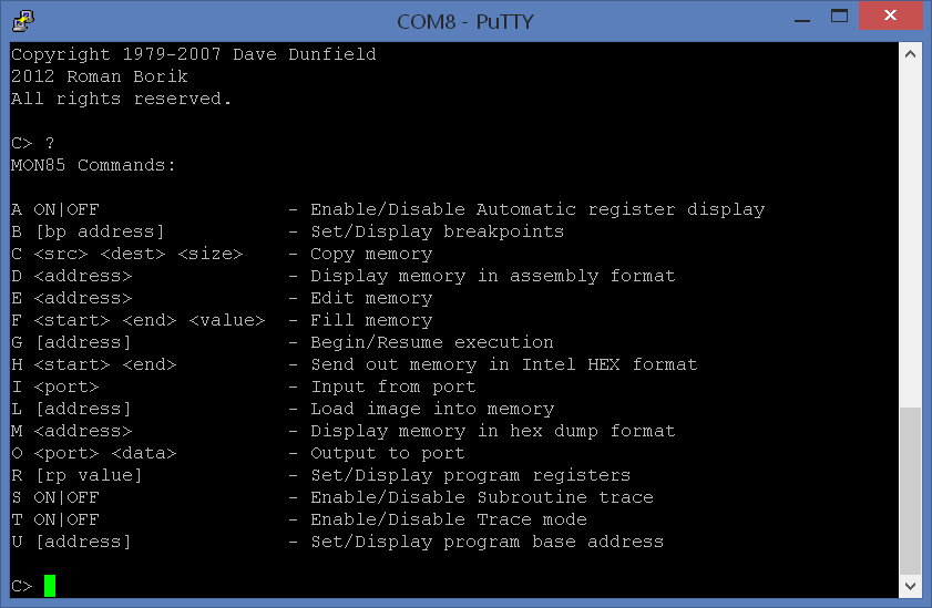
MiniMax8085 uses MON85 Software Debug Monitor For the 8085/8080 written by Dave Dunfield. Specifically it was tested with the improved by Roman Borik version 1.2. This version adds support for undocumented 8085 instructions and flags.
The famous Tiny BASIC 2.0 written by Li-Chen Wang and modified by Roger Rauskolb, runs on MiniMax8085 with very little modifications: The 8251 USART I/O address needs to be updated, and its initialization parameters need to be slightly updated to use 1 stop bit instead of two, and to enable CTS/RTS flow control. Also the RAM addresses need to be updated to start from 8000h.
IMSAI 8K BASIC runs on MiniMax8085 with minimal modifications (memory and USART I/O addresses), and provides floating point support. With that being said, it is slower that Tiny BASIC.
The code below blinks an LED connected to 8085's SOD output. The code is borrowed from Glitch Works 8085 SBC project
;Assembly                                 Address    Opcode

;Flash a LED on SOD


;Load C000h to SP
START:          LXI     H,0C000h        ; 0000       21 00 C0
                SPHL                    ; 0003       F9


FLASH:          MVI     A,0C0h          ; 0004       3E C0
                SIM                     ; 0006       30
                CALL    DELAY           ; 0007       CD 13 00
                MVI     A,40h           ; 000A       3E 40
                SIM                     ; 000C       30
                CALL    DELAY           ; 000D       CD 13 00
                JMP     FLASH           ; 0010       C3 04 00

;Delay, return to HL when done.
DELAY:          MVI     A, 0FFh         ; 0013       3E FF
                MOV     B,A             ; 0015       47
PT1:            DCR     A               ; 0016       3D
PT2: DCR B ; 0017 05This code prints "8085" to the serial port, and then echoes received characters.
; USART registers
USART_DATA     EQU     08h
USART_CMD      EQU     09h

START:         LXI     H,0C000h
               SPHL
               CALL    USART_INIT

; write a banner
               MVI     A,38h           ; '8'
               MOV     C,A
               CALL    USART_OUT
               MVI     A,30h           ; '0'
               MOV     C,A
               CALL    USART_OUT
               MVI     A,38h           ; '8'
               MOV     C,A
               CALL    USART_OUT
               MVI     A,35h           ; '5'
               MOV     C,A
               CALL    USART_OUT
               MVI     A,0Dh           ; CR
MOV C,AThe provided source code can be built using the AS macroassembler Here are steps to compile the code, assuming Windows host, and that AS installed in *C:\asw* folder:
See 3D Printable Enclosure for MiniMax8085 page for the instructions, STL files, OpenSCAD source.
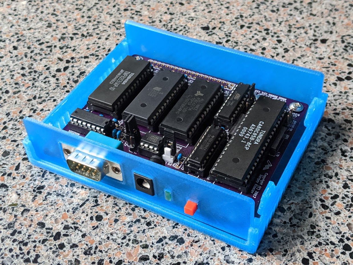
The Keypad and VFD (vacuum fluorescent display) extension board provides simple 20-key keypad and display for MiniMax8085 SBC.
The Arithmetic Processor and Extension board adds to MiniMax 8085 SBC an AMD Am9511A / Intel 8231A Arithmetic Processor Unit (APU), Intel 8255 Programmable Parallel Interface (PPI), Intel 8254 Programmable Interrupt Timer (PIT), and switchable 32 KiB SRAM, that can swapped in instead of MiniMax 8085 on-board ROM
| Qty | Value | Footprint | References |
|---|---|---|---|
| 6 | 0.1uF | my_components:Cap_Cer_508 | C1, C2, C3, C4, C5, C6 |
| 5 | 0.1uF | my_components:Cap_Pol_508_3 | C7, C8, C9, C10, C11 |
| 4 | CONN_1 | my_components:Hole_3mm | HOLE1, HOLE2, HOLE3, HOLE4 |
| 2 | 33pF | my_components:Cap_Cer_508 | C14, C15 |
| 2 | 4.7k | my_components:Conn_SIL6 | RR1, RR2 |
| 1 | 100k | my_components:Res_762 | R3 |
| 1 | 10uF | my_components:Cap_Pol_508_3 | C13 |
| 1 | 1N4148 | my_components:Diode_762 | D1 |
| 1 | 1uF | my_components:Cap_Pol_508_3 | C12 |
| 1 | 27C128 | my_components:IC_DIP28_600 | U3 |
| 1 | 33 | my_components:Res_762 | R1 |
| 1 | 470 | my_components:Res_762 | R2 |
| 1 | 6.144MHz | my_components:Crystal_HC-49U_Vert | Y1 |
| 1 | 62256 | my_components:IC_DIP28_600 | U4 |
| 1 | 74HC573 | my_components:IC_DIP20_300 | U6 |
| 1 | 80C85A | my_components:IC_DIP40_600 | U1 |
| 1 | 82C51A | my_components:IC_DIP28_600 | U2 |
| 1 | CLK | my_components:Conn_Pin_Header_3x1_2.54mm | JP3 |
| 1 | DS1210 | my_components:IC_DIP8_300 | U8 |
| 1 | EXTENSION | my_components:Conn_Pin_Header_20x2_2.54mm | P4 |
| 1 | GAL16V8 | my_components:IC_DIP20_300 | U5 |
| 1 | MAX232A | my_components:IC_DIP16_300 | U7 |
| 1 | OSHW-logo_silkscreen-front_10mm | OSHW-logo:OSHW-logo_silkscreen-front_10mm | G*** |
| 1 | POWER | my_components:Conn_Power_Jack_Circular_Pads | P1 |
| 1 | PWR | my_components:LED_Dialight_566-0206F | D2 |
| 1 | RESET | my_components:Switch_Tactile_6mm_Right | SW1 |
| 1 | ROM_1 | my_components:Conn_Pin_Header_3x1_2.54mm | JP1 |
| 1 | ROM_27 | my_components:Conn_Pin_Header_3x1_2.54mm | JP2 |
| 1 | SERIAL | my_components:Conn_Dsub_DE9M | P3 |
| 1 | SIO | my_components:Conn_Pin_Header_3x1_2.54mm | P2 |
| 1 | VBAT | my_components:Conn_Friction_Lock_2P_2.54mm | P5 |

tebl/BulkyMIDI-32
A HW build of the MT32-PI project, allowing you to emulate a Roland MT-32 using a Raspberry Pi. Includes enough additional modules to build a MIDI-mountain as well as adapters for connecting to most things retro.

hkzlab/pontag
PONTAG is an active adapter that converts a mouse using PS/2 protocol into an RS232 mouse (Microsoft protocol), commonly used on IBM XT/AT and compatibles.


ricaflops/Jupiter-II-Expansion
Expansion board for Jupiter-II computer


It measures 100 × 80 mm and has 2 copper layers, 1.6 mm thick.
45 parts, built around the MAX232ACSE+, 27C128-15 and 74HC573. The full list of its parts is on this page, with links to each part's symbol and footprint where PCBKit's library has them.
From the skiselev/minimax8085 repository on GitHub, at the commit this page was made from: the board is KiCad/Mini8085.kicad_pcb. PCBKit opens the board in the browser, with nothing to install.
Its repository publishes it under the GPL-3.0 licence: you may reuse it on that licence's terms (keep the author's notice, and for a copyleft licence share your changes alike).