
4 layers40 × 14 mm
Rs probe
probe-rs/rusty-probe
This is an open hardware probe for the Serial Wire Debug (SWD) and JTAG protocol. Based on the RP2040 MCU.
108 parts170

 probe-rs/hs-probe145
This is an open hardware probe for the Serial Wire Debug (SWD) and JTAG protocol. It utilizes an STM32F723 MCU which has an USB 2.0 High-speed Phy.
Hs probe is an open-source printed circuit board by probe-rs, from the probe-rs/hs-probe repository on GitHub. It is a 4-layer board of 40 × 14 mm with 57 parts on 138 nets, routed with 961 tracks and 162 vias.
It is built around the LTST-C19HE1WT. Its parts include 26 capacitors, 15 resistors, 7 ICs, 5 connectors and 2 diodes. It belongs with the sensors and measurement and interfaces and adapters boards and the STM32 boards of this library.
This is an open hardware probe for the Serial Wire Debug (SWD) and JTAG protocol. It utilizes an STM32F723 MCU which has an USB 2.0 High-speed Phy.
The firmware is available here and is open-source: https://github.com/probe-rs/hs-probe-firmware
There is an USB MUX on the board, so when the probe starts it enumerates in USB FS where one can access the internal bootloader, and then when the firmware takes over it can switch to the USB HS.
The schematic can be found in the schematic PDF.
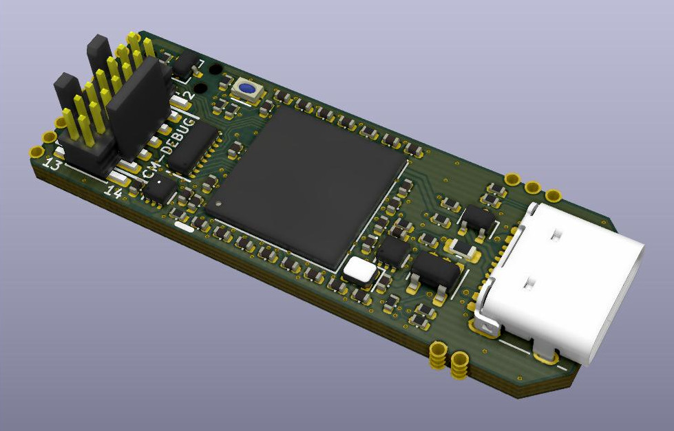
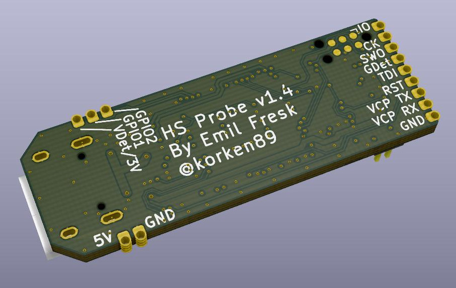
The hs-probe package sold on our shop contains two 16 wire ribbon cables, three 14p connectors and one 10p connector. You can make one cable with a 14p connector on each side and one cable with a 14p connector on one and a 10p connector on the other side. How to align the connectors is explained in the image below:
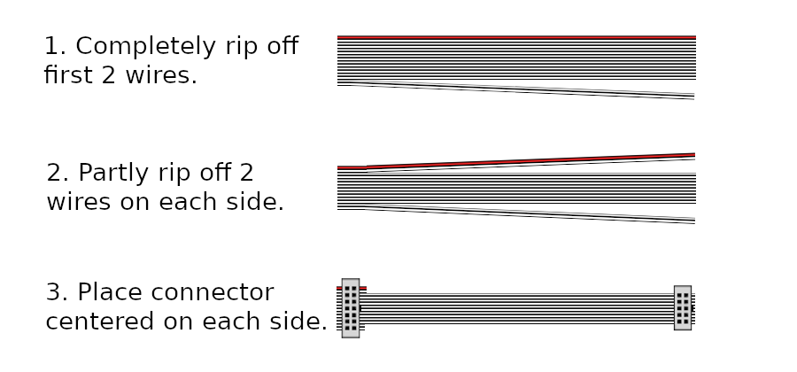
This work is licensed under CERN-OHL-P.
| Qty | Value | Footprint | References |
|---|---|---|---|
| 16 | 0.1u | passive:C_0402 | C3, C8, C9, C11, C12, C13, C14, C15, C16, C17, C18, C19, C20, C21, C22, C23 |
| 10 | 2.2u | passive:C_0402 | C1, C2, C4, C5, C6, C7, C24, C25, C26, C27 |
| 8 | 5.1k | passive:R_0402 | R1, R3, R4, R10, R101, R102, R103, R104 |
| 5 | 3k | passive:R_0402 | R2, R5, R6, R7, R9 |
| 2 | 39 | passive:R_0402 | R8, R11 |
| 2 | MIC5353 | dfn:DFN-6-1EP_1.6x1.6mm_P0.5mm_EP0.5x1.26mm | U3, U7 |
| 1 | DMP2110UW-7 | sot:SOT-323 | Q101 |
| 1 | 12 MHz | crystals:Crystal_4Pin_2.0x1.6mm | U2 |
| 1 | Castellated Vias | connectors:1x3_1.5mm_castellated | J4 |
| 1 | Castellated Vias | connectors:1x2_1.5mm_castellated | J3 |
| 1 | Castellated Vias | connectors:1x9_1.5mm_castellated | J2 |
| 1 | ESD7002WTT1G | sot:SOT-323 | D2 |
| 1 | Fuse_Small | Fuse:Fuse_0603_1608Metric | F101 |
| 1 | LTST-C19HE1WT | LED_SMD:LED_LiteOn_LTST-C19HE1WT | D1 |
| 1 | MAX40203AUK or MAX40200AUK | sot:SOT-23-5 | U6 |
| 1 | NUF8401MNT4G | dfn:DFN-16-1EP_1.6x4mm_P0.5mm | U4 |
| 1 | STDC14 | connectors:PinHeader_2x07_FTSH-107-01-L-DV-K | U5 |
| 1 | USB_C_Receptacle_USB2.0 | connectors:USB_C_Receptacle_USB4105 | J1 |
| 1 | hs-probe-stm32 | bga:UFBGA-201_10x10mm_Layout15x15_P0.65mm | U1 |
| 1 | tag-connect-swd | Connector:Tag-Connect_TC2030-IDC-NL_2x03_P1.27mm_Vertical | J5 |
It measures 40 × 14 mm and has 4 copper layers, 1.6 mm thick.
57 parts, built around the LTST-C19HE1WT. The full list of its parts is on this page, with links to each part's symbol and footprint where PCBKit's library has them.
From the probe-rs/hs-probe repository on GitHub, at the commit this page was made from: the board is hs-probe.kicad_pcb. PCBKit opens the board in the browser, with nothing to install.
Its repository states no licence, so its author keeps all rights: ask probe-rs before reusing the design.
probe-rs/rusty-probe
This is an open hardware probe for the Serial Wire Debug (SWD) and JTAG protocol. Based on the RP2040 MCU.

NabuCasa/yellow
Home Assistant Yellow - hardware for Home Assistant which grows with your needs.


