2 layers191.8 × 140.3 mm

 PatrickAJoseph/bluetooth-daq
A simple low-speed Bluetooth enabled DAQ
Bluetooth daq digital submodule is an open-source printed circuit board by PatrickAJoseph, from the PatrickAJoseph/bluetooth-daq repository on GitHub. It is a 2-layer board of 150 × 150.9 mm with 142 parts on 103 nets, routed with 1,230 tracks and 180 vias.
It is built around the SN75176AD, 74HC165D and 74HC595, with the CD4053BE, 24LC1025-I/P and SMAJ5.0CA among its other parts. Its parts include 54 capacitors, 52 resistors, 8 ICs, 7 diodes and 5 connectors. It belongs with the radio and wireless boards of this library.


A simple low-speed Bluetooth enabled DAQ consisting of HV/LV voltage, current measurement, LV analog I/O, resistance measurement, UART, I2C & SPI communication interfaces and a high speed ADC combining multiple functionalities within one device. The device can be operated through a mobile/PC application via Bluetooth or through RS-485 interface. 16 devices can be connected to the RS-485 interface.
Reduce the number of induvidual electronic test equipment required for electronic hardware/software development.
Combine commonly used electronic test functions within a single device
Enable versatile interface to the device (RS485, Bluetooth, Web) and test automation support to reduce effort of manual testing.
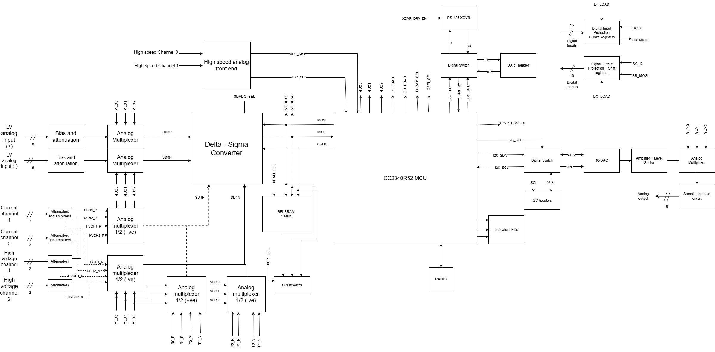
The device provides 2 high voltage analog inputs with a range of +/- 50V and maximum input frequency of 200 Hz. The high voltage analog input front end attenuates the input voltage signal and adds bias to meet voltage level requirements of the sigma-delta ADC inputs.
The device provides 2 current inputs with common mode voltage upto +/- 50V and a range of +/- 3A. The voltage drop across the current measurement terminal is 0.1V/A.
The device provides 8 channel +/- 15V low voltage analog inputs. Maximum input frequency per channel is set to 200 Hz.
The device provides 2 channel resistance measurement feature. The supported resistance measurement range is 1 ohm to 1 MOhm.
The device provides 2 single ended high speed analog signal acquisition channels with sampling frequency of 200 kSPS per channel, limiting the combined input signal frequency to 10kHz.
The device provides 2 thermistor temperature measurement channels. The reference voltage for the thermistor interface is 3.3V and reference resistance is 10k. The device comes with a calibration table for a 10K NTC. If user uses any other NTC, then, the calibration table for thermistor has to be manually entered by the user via software.
The heart of most of the analog to digital conversions is carried out by a 24-bit sigma-delta ADC (ADS131M02: https://www.ti.com/lit/ds/symlink/ads131m02.pdf?ts=1769953054375&ref_url=https%253A%252F%252Fwww.ti.com%252Fproduct%252FADS131M02).
The input to each channel of the ADC is multiplexed with the help of analog multiplexer (CD4051: https://www.ti.com/lit/ds/symlink/cd4051b.pdf)
The device provides 8 analog outputs with range +/- 10V. Since a sample and hold circuit is used at the output stage, the output current limit is 1mA and so an external buffer must be used. The DAC used in the solution is DAC101C081 (https://www.ti.com/product/DAC101C081)
The device uses a 1 MBit SRAM to store samples acquired from various modules such as high speed ADC, digital inputs, digital output patterns etc. The SRAM used is 23LCV1024 (https://ww1.microchip.com/downloads/en/DeviceDoc/25156A.pdf)
The device provides 16 digital inputs and digital outputs. The digital inputs are read by the MCU through a 74HC165 shift register (https://www.ti.com/lit/ds/symlink/sn74hc165.pdf) and the digital outputs are transferred through 74HC595 shift register (https://www.ti.com/lit/ds/symlink/sn74hc595.pdf).
The digital inputs have a range of +/- 3.3V in order to provided reverse voltage protection. The digital outputs have a current limit of 5mA per channel.
There are three indicator LEDs, 1 green, 1 red and 1 yellow. The green LED indicates status of any ongoing communication between host and the device. The red LED indicates any error which has occured in the device. The yello LED indicates that a firmware upgrade is going on the device.
The microcontroller used in the device is CC2340R52 (https://www.ti.com/product/CC2340R5/part-details/CC2340R52E0RGER) which is an ARM Cortex-M0+ MCU with 512 KB FLASH and 36 KB RAM.
The device provides an SPI, I2C and a UART interface which can be used by the user to transfer bytes to external devices under test.
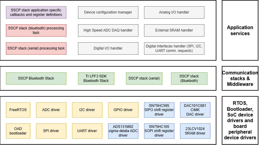
The software uses FreeRTOS operating system. This is required by the TI Bluetooth Stack and also for multithreading purposes.
The following SoC peripheral drivers are required by the product.
| Driver | Description |
|---|---|
| ADC | Required by the high speed analog input module |
| SPI | Required for accessing the shift registers and the external SRAM memory |
| I2C | Required to control DAC IC on the board |
| UART | Required for interaction with host PC through RS-485 interface |
| GPIO | Required by all other drivers |
| Driver | Purpose |
|---|---|
| ADS131M02 | Controls the 24-bit Sigma-Delta ADC. Performs common operations such as setting ADC PGA gain, calibration, sample acquisition etc. |
| SN75HC595 | Write data to the digital outputs through shift registers |
| SN75HC165 | Read data from the SOPI shift registers |
| DAC101C081 | Required for controlling the external 10-bit for setting the desired output voltage. Also, supports calibration. |
| 23LCV1024 | Controls the external SRAM IC. Provides read and write APIs for the external memory |
The device supports over the air firmware upgrade through the TI Simplelink Connect application for Mobile (https://www.bing.com/search?q=TI+Simplelink+connect&cvid=ed73fef019854968bf1f31853ef2398b&gs_lcrp=EgRlZGdlKgYIABBFGDkyBggAEEUYOTIGCAEQABhAMgYIAhAAGEAyBggDEAAYQDIGCAQQABhAMgYIBRAAGEAyBggGEAAYQNIBCDMyNjZqMGo5qAIIsAIB&FORM=ANAB01&PC=U531). Firmware upgrade over Bluetooth is only supported for mobile phones and not for laptop.
The device uses the Texas Instruments Bluetooth stack. This stack is required for Bluetooth over the air firmware upgrade and also serves as an interface between the mobile/PC and the device.
The SSCP (Simple System Control Protocol) is the transport protocol which is used by the device to interact with the host via serial interface or Bluetooth. Each interface requires a seperate SSCP responder stack instance. For more details about the SSCP protocol refer to the following Git repository: https://github.com/PatrickAJoseph/simple-system-control-protocol.
This software component defines the register callback functions, register definitions related to the application for the SSCP stack.
This software components receives bytes from the interface (serial/Bluetooth) and sends the received byets to the SSCP stack for processing.
Validates the configuration provided by the user. Also, stores and loads device settings in non-volatile storage.
Acquires samples from the high speed acquisition ADC channels and stores conversion results in the external SRAM. Users can then read back the samples stored in the SRAM.
Used to control the digital inputs and the digital outputs of the device through the shift registers as described in the hardware section. Supports setting, clearing, toggling each DO pin and reading state of DI pins.
Controls calibration of each high voltage analog input channel, current channel, resistance measurement channel, thermistor temperature measurement channel and analog output channel. Acquires samples from the analog input channels, performs filtering and then adds calibration parameters to provide processed results. Manages the multiplexing of different analog inputs to the input channels of the sigma-delta converter through the multiplexer.
The external SRAM handler is an abstraction component for the external SRAM driver. Responsible for reading and writing data application defined memory regions in the external SRAM memory via the SPI interface.
Used to handle received communication interface commands (such as transmit, receive commands) for UART, I2C and SPI protocols. Can handle multiple byte transfer for all interfaces and stores received bytes in the external SRAM for post processing.
| Qty | Value | Footprint | References |
|---|---|---|---|
| 32 | 100p | Capacitor_SMD:C_0805_2012Metric_Pad1.18x1.45mm_HandSolder | C1, C2, C3, C10, C11, C12, C13, C14, C15, C16, C29, C30, C31, C32, C33, C34 +16 |
| 32 | 620 | Resistor_SMD:R_0805_2012Metric_Pad1.20x1.40mm_HandSolder | R1, R2, R10, R11, R12, R13, R14, R15, R16, R18, R19, R20, R21, R22, R23, R24 +16 |
| 16 | D_Schottky | Diode_SMD:D_SMA_Handsoldering | DIP0, DIP1, DIP2, DIP3, DIP4, DIP5, DIP6, DIP7, DIP8, DIP9, DIP10, DIP11, DIP12, DIP13, DIP14, DIP15 |
| 9 | 10k | Resistor_SMD:R_0805_2012Metric_Pad1.20x1.40mm_HandSolder | R17, R26, R27, R41, R42, R43, R49, R57, R200 |
| 8 | 100n | Capacitor_SMD:C_0805_2012Metric_Pad1.18x1.45mm_HandSolder | C17, C20, C23, C37, C48, C51, C54, C56 |
| 8 | 1u | Capacitor_SMD:C_0805_2012Metric_Pad1.18x1.45mm_HandSolder | C18, C21, C24, C38, C49, C52, C55, C57 |
| 7 | SMAJ5.0CA | Diode_SMD:D_SMA_Handsoldering | D33, D34, D35, D36, D37, D38, D39 |
| 6 | 10u | Capacitor_SMD:C_0805_2012Metric_Pad1.18x1.45mm_HandSolder | C19, C22, C25, C39, C50, C53 |
| 4 | 22 | Resistor_SMD:R_0805_2012Metric_Pad1.20x1.40mm_HandSolder | R48, R51, R53, R55 |
| 2 | 1k | Resistor_SMD:R_1206_3216Metric_Pad1.30x1.75mm_HandSolder | R39, R40 |
| 2 | 2.2k | Resistor_SMD:R_0805_2012Metric_Pad1.20x1.40mm_HandSolder | R58, R59 |
| 2 | 33 | Resistor_SMD:R_0805_2012Metric_Pad1.20x1.40mm_HandSolder | R45, R47 |
| 2 | 74HC165 | SN74HC165_custom:D16 | U3, U4 |
| 2 | 74HC595 | Package_SO:SOIC-16_3.9x9.9mm_P1.27mm | U1, U2 |
| 2 | CD4053B | CD4053BE_custom:D16 | U7, U8 |
| 1 | 120 | Resistor_SMD:R_1206_3216Metric_Pad1.30x1.75mm_HandSolder | R38 |
| 1 | 24LC1025 | 23LCV1024:SOIC8-N_MC_MCH | U5 |
| 1 | Communication I/F | Connector_PinHeader_2.54mm:PinHeader_2x08_P2.54mm_Vertical | J4 |
| 1 | Digital Inputs | Connector_PinHeader_2.54mm:PinHeader_2x08_P2.54mm_Vertical | J2 |
| 1 | Digital Outputs | Connector_PinHeader_2.54mm:PinHeader_2x08_P2.54mm_Vertical | J3 |
| 1 | MCU I/F | Connector_PinHeader_2.54mm:PinHeader_2x08_P2.54mm_Vertical | J1 |
| 1 | RS-485 I/F | Connector_Phoenix_MC_HighVoltage:PhoenixContact_MCV_1,5_2-G-5.08_1x02_P5.08mm_Vertical | J5 |
| 1 | SN75176AD | Package_SO:SOIC-8_3.9x4.9mm_P1.27mm | U6 |
It measures 150 × 150.9 mm and has 2 copper layers, 1.6 mm thick.
142 parts, built around the SN75176AD, 74HC165D, 74HC595 and CD4053BE. The full list of its parts is on this page, with links to each part's symbol and footprint where PCBKit's library has them.
From the PatrickAJoseph/bluetooth-daq repository on GitHub, at the commit this page was made from: the board is hardware/digital_submodule/bluetooth-daq-digital-submodule/bluetooth-daq-digital-submodule.kicad_pcb and its schematic hardware/analog_submodule/analog_submodule/analog_submodule.kicad_sch. PCBKit opens the board in the browser, with nothing to install.
Its repository states no licence, so its author keeps all rights: ask PatrickAJoseph before reusing the design.


felipesantiagoach-ops/cdp1802-8bit-computer
8-bit microcomputer based on the RCA CDP1802, the first CMOS microprocessor. Three stages designed in KiCad: two built and tested (assembly programs, UART, Tiny BASIC, Elf/OS) and a final design with an ADC, I²C/SPI…


MR-DOS/MWGEN-G1
12.5 MHz - 6400 MHz (LMX2572) or even up to 20 GHz (LMX2595) generator board with int./ext. reference.


ay2718/RadomeMotorController
The Radome CAN protocol is very simple. Send azimuth commands to address 0x1 and elevation commands to address 0x2. Azimuth and elevation reply back from addresses 0x101 and 0x102 respectively.


Aiyin4Da-2/Main_Ctrl_H7
STM32H723VGT6 MainCtrlBoard Author: Aiyin4DaGLD · Hardware: v1.2 · Updated: 2026-08-21