
4 layers40 × 40 mm

 njcoburn/OPENIMAGESENSOR
OPENIMAGESENSOR - An open source image sensor.
Tester dock is an open-source printed circuit board by njcoburn, from the njcoburn/OPENIMAGESENSOR repository on GitHub, published under the Apache-2.0 licence. It is a 4-layer board of 100 × 80 mm with 81 parts on 39 nets, routed with 1,098 tracks and 103 vias.
It is built around the SN74LVC244APW, OPA2320AID and ADS1115IDGSR. Its parts include 35 resistors, 28 connectors, 8 capacitors and 4 ICs.


Current — completed results checkpoint, 4 October: all 18 selected five-device bank cases passed, with 36 transients and 3,456 reference calculations. The sequence finished 2 October at 15:11 Pacific after 48 h 21 min; no verification jobs remain active. Worst total/tracking errors are 456.591/215.322 µV against 500 µV; sample refinement is 0.465218 µV against 10 µV. This is selected coverage of a one-row, 64-column bank, not full-chip qualification. Next: define bounded supply/wiring/placement checks before real drivers and multirow integration. Resume here · Completion record · Overview. Earlier status entries below are historical.
Latest review, 30 September — stopped; no active simulations: all three 100 ns runs and 576 references completed and are independently audited. All three 50 ns runs hit the four-hour timeout, leaving 11 of 384 output samples unverified. Coarse typical/SS totals are 391.959/445.375 µV, but FF is 602.413 µV against 500 µV. 7 available fine FF samples also exceed the limit (up to 577.376 µV). No complete pair is qualified and the later queue did not start. Next: address remaining fast-corner capture/storage error and use a longer watchdog for reruns. Reviewed evidence · Handoff. Earlier running/completion statements below are historical.
Running, 30 September — 64-column candidate sequence: checkpoint and
changelog were pushed as 06889e5 before this work. The new physical 64-column
bank passes DRC/LVS and all capture-chain checks. Six typical/SS/FF 125 °C
simulations are running, with 576 matched references planned for this batch.
On audited passes, the controller advances through mixed corners, 27 °C cases,
and remaining typical-process illumination patterns (18 cases / 36 transients /
3,456 references in the complete queue). Failure stops subsequent stages.
Live overview · Status.
Earlier status entries below are historical.
Latest, 30 September — physical candidate verified: the three-device capture switch is implemented in a separate column and two-column bank. DRC/LVS and 40 µm abutment pass. With 12.5 µs acquisition, extracted typical/SS/FF worst total errors are 152.197/181.071/258.782 µV across port/far placement (limit 500 µV). Placement sensitivity is below 0.044 µV. This stage completed 18 transients and 108 references. Next: separate 64-column candidate build and process validation. No simulation jobs remain active; the old 64-column checkpoint is unchanged. Physical candidate and rerun guide · Handoff. Earlier status entries below are historical.
Latest, 30 September — candidate cycle tests reviewed: 20 transients and 120 references are complete. Three series NMOS capture devices pass the selected two-column typical/SS/FF screen; FF error improves from 1240.756 to 410.653 µV (limit 500 µV). A separate 12.5 µs acquisition test improves SS settling. Next: check the combined changes, implement a separate physical column revision, verify extraction/DRC/LVS and small-bank behavior, then repeat full-bank corners. The current GDS and its known process failures remain unchanged. No jobs are active. Results and rerun guide · Handoff. Earlier status entries below are historical.
Diagnosis completed, 30 September: the process failures are reviewed and short current/candidate tests are complete. FF retention is dominated by the NMOS capture switch in the probed states; series devices reduce DC leakage but are not yet a validated correction. Next: candidate capture/readout transients and an SS acquisition-timing test. No new long batch is active. Diagnosis and plots · Handoff.
Current, 30 September: the SS/FF process batch finished. Both total-error checks fail (512.924 / 2000.323 µV vs 500 µV); other selected checks pass. All 384 references are audited and 1,740 evidence files verify. Next is diagnosis of SS output settling and FF storage retention, before more corner coverage. Review · Handoff. Earlier active-job descriptions below are historical.
Active, 30 September: the first SS/FF MOS-process batch is running at 125 °C inverse illumination: four 100/50 ns transients and 384 planned references, with an independent watcher. The small FF control failed capture/storage accuracy; that failure is retained while measuring the actual 64-column layout. Results are pending. Overview journal · Profile and scope · Handoff.
Verification journal and rerun guide explains every test, records results and tracks what is needed for repeatable pixel-layout experiments.
Completed and reviewed, 30 September: bright illumination and the authorized joint parasitic-placement batch both pass. All five illumination patterns now pass at 27/125 °C: 20 transients and 1,920 independent references, plus four placement transients and 384 references. Those baseline jobs are complete; the process batch above is active. Next: process/wire/supply corners and remaining placement/local-supply checks, then real drivers and repeated rows. Full-chip qualification remains open. Completion review · Handoff.
Current goal: 64×64 first silicon on wafer.space GF180, with modest frame rate. Completion plan · Next steps · Handoff
Overnight results: bright total error is 359.158/402.995 µV at 27/125 °C against 500 µV. Joint relocation of 67 conserved shunts passes at 27 °C alternating and 125 °C inverse; the largest HOLD/STORE change is 1.527 µV against 10 µV. Bright and placement took 3.97 and 3.87 hours respectively, including audits. All ten simulation/audit containers exited successfully.
Completed and reviewed, 29 September: uniform dark passes at 27/125 °C: 248.852/411.912 µV worst total error against 500 µV, with four completed transients and 384 audited references. The batch finished in 4.04 hours. Nothing from this batch is still running; middle and bright have also passed as described above. Uniform results.
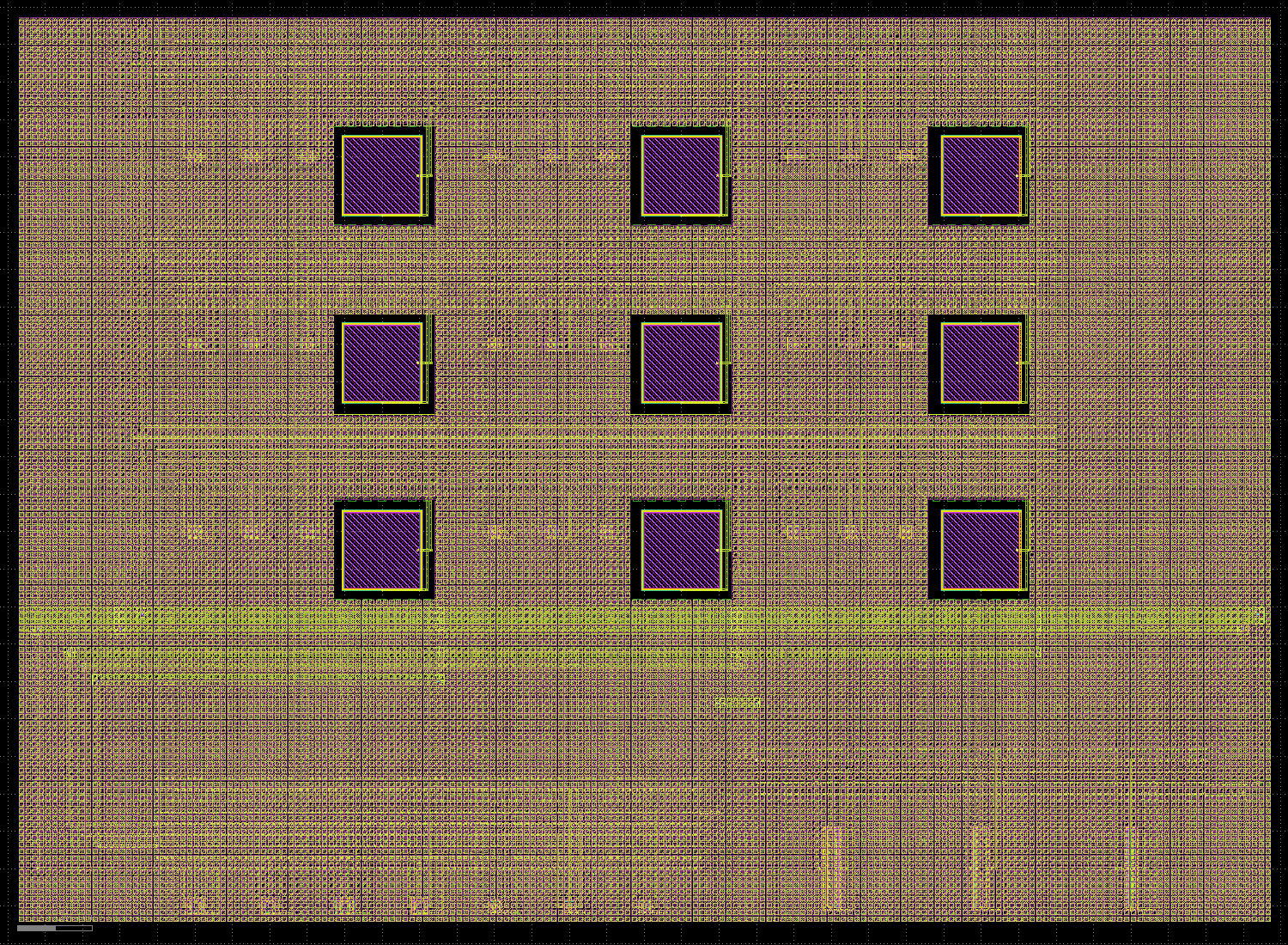
View the current device layout — labeled GDS and close-up of the implemented 64-column bank plus one pixel row, measuring 2.668 × 1.070 mm. Exact GDS checkpoint. The full 64×64 chip remains to be assembled.
Latest, reviewed 29 September: the complete alternating/inverse matrix now passes at both 27 °C and 125 °C. The new 27 °C inverse / 125 °C alternating cases reach 387.179/430.383 µV worst total error, below 500 µV. All eight matrix transients and 768 references are audited; maximum saved-sample refinement is 0.150 µV, below 10 µV. All 1,707 distinct new evidence files verify. The jobs and auditor finished successfully; the completed uniform-dark batch is described above. Temperature/pattern matrix
Completed, 28 September: both earlier complete 64-column bank screens pass. All four transients finish 128 reads each, with 384 independently audited references across the nominal alternating and hot inverse cases. Worst total error is 372.606 µV at 27 °C / 438.213 µV at 125 °C, below 500 µV; maximum saved-sample 100/50 ns difference is 0.133 µV, below 10 µV. All 1,711 distinct evidence files verified. The jobs and auditor have finished successfully.
All five illumination patterns at both temperatures now pass. Remaining corner/placement coverage precedes real drivers and repeated rows. Full-chip qualification remains open. Results and plots · Current handoff
Previous electrical results, 27 September:
The 16-column extension passes its selected checks across 46 transients and 1,152 references. Worst total error is 433.171 µV and tracking is 301.667 µV (500 µV limits). All five patterns at 27/125 °C have 100/50 ns comparisons; the largest saved-terminal difference is 0.450 µV. All 19 individual shunts plus their joint placement pass for the hot inverse pattern, with 0.105/0.137 µV maximum HOLD/STORE changes (10 µV limit). The separate inverse-pattern layout–schematic response reaches 10.062 mV and has no assigned acceptance threshold.
The 8 µm bus alone does not solve 64-column scaling: a matched column-62 readout fails at 1,994.440 µV total error. A new physical distributed ground return fails with 10 µs acquisition at 547.178 µV total error and 340.253 µV tracking. Both main DRC checks and both LVS paths pass, and a geometry audit restricts the change to ground metal/vias. The new bank is 2667.87 × 1069.80 µm, within the 2700 × 1100 µm budget. See the selected readout comparison and capture/ground diagnosis.
Extending acquisition from 10 to 12 µs on that same grid passes the selected diagnostic at 269.281 µV total error and 62.529 µV tracking. Only the ACQ falling edges and sample times move; selection/reset and the 20 µs slot budget stay unchanged. Three new matched references and an unchanged-prefix comparison are audited. The separately versioned full-bank runner now supports this timing. The original attempts were stopped on 27 September; the resumed nominal/hot inverse pairs now pass their complete selected audits. See PICK_UP_HERE.md for results and the next coverage batch.
These are bounded development screens. Full 16-column corner/placement coverage, remaining full-bank corners/individual placements, real drivers, repeated rows and exact 64×64 manufacturing qualification remain open.
Original geometry constraint: the older array and bank do not fit a standard full slot. The compact pixel/bank work above addresses that block-size constraint. The new 40 µm-pitch floorplan budget fits the published default core as planning rectangles; it is not qualified GDS. The full 64×64 chip is not yet assembled.
The extracted 64-pixel row and isolated physical capture column have passing electrical evidence. The physical bank passes scoped DRC/LVS, but coupled readout, multirow operation, real drivers and final-chip signoff remain open. Docker access is restored. The new 40 µm compact pixel and 2×2 control pass main DRC and both LVS paths; the 2×2 nominal/hot electrical screens and timestep checks pass. The reset follow-up passes 12 transients and extended references using audited shunt placements; the raw isolated extraction remains diagnostic. The original raw/reduced full-bank initialization timed out in four bounded controls before the later KLU continuation resolved startup. The new compact capture column fits 40 µm pitch and passes scoped DRC/LVS, adjacent-column spacing, 60 transients and 36 references. The physically joined tile now passes 54 transients and 72 references, with 419.404 µV worst total capture/readout error. The shared two-column bank now passes both main DRC/LVS paths, 100 transients and 240 references (419.033 µV worst total error). It includes physical reference MOS and shared buses; the later 1×64 work is above. The separate layout–schematic integrated-response difference reaches 5.821 mV. A separate 3×3 tapeout is not a prerequisite.
The dated entries below retain earlier evidence and historical release targets. Use the completion plan above for current priorities.
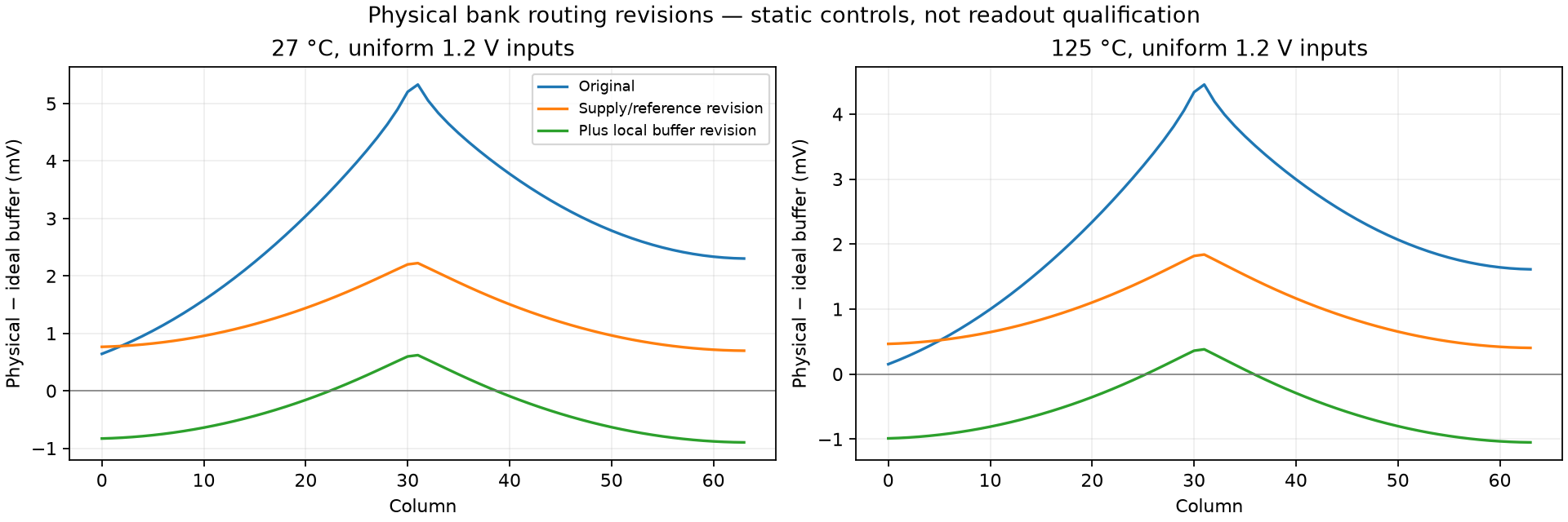
Latest physical result: Reinforced supply/reference and local buffer routing passes both main DRC checks and both LVS paths. Worst nominal/hot static buffer shift across 1.2–2.0 V falls from 5.331 to 1.320 mV; all 16 selected DC controls complete. The coupled reset test still times out during initialization; full readout remains unqualified. Measured comparison and tradeoffs.
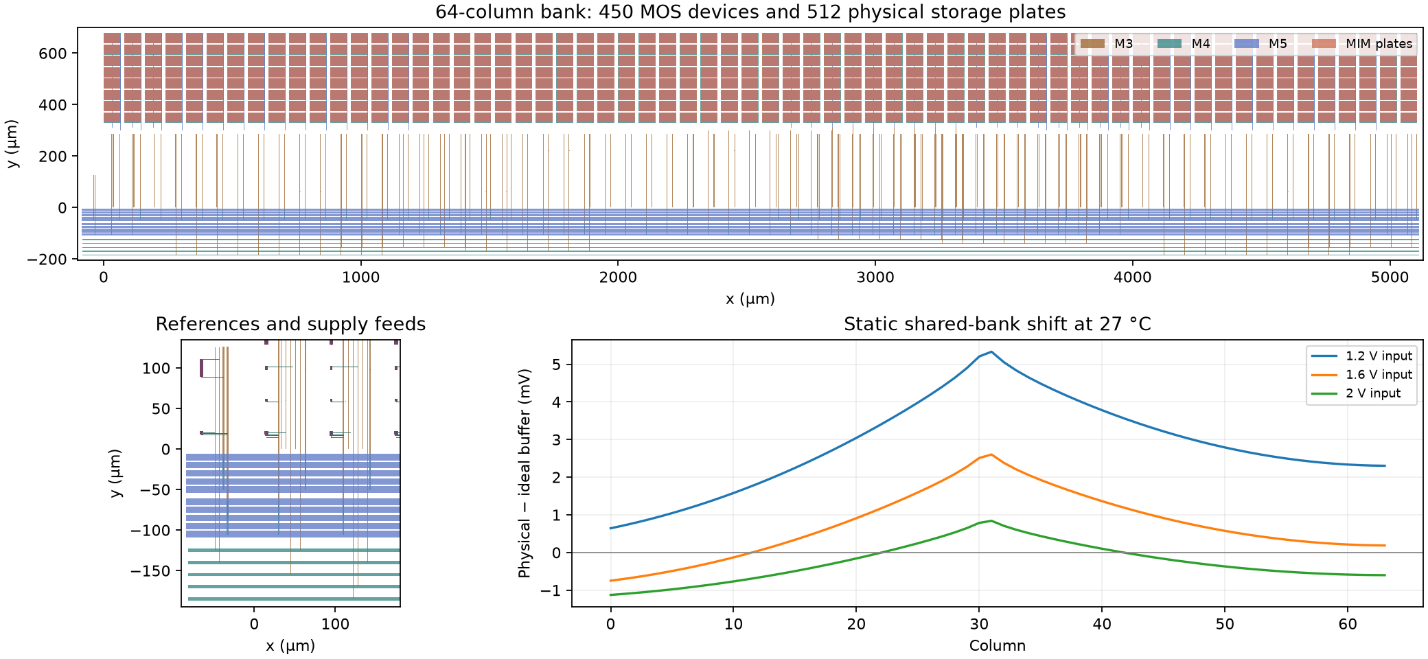
Earlier physical result: The shared 64-column capture bank passes Magic/KLayout main DRC and both LVS paths: 450 MOS devices, 512 storage plates and fully extracted shared routing. Isolated DC controls reveal millivolt-scale spatial shifts; coupled-row accuracy is not yet qualified. Bank measurements and scope.
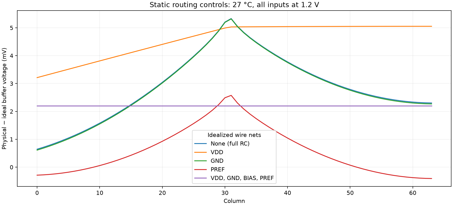
Earlier diagnosis: Eight DC controls implicate VDD/PREF routing in the spatial spread; idealizing supplies/references still leaves a 2.199 mV common offset. Full readout qualification remains open. Measured controls and reset diagnostics.
Earlier isolated-column result: The isolated capture/readout column passes all 48 nominal/hot simulations, Magic/KLayout main DRC and both LVS paths. Worst tracking error is 176.560 µV (limit 500); timestep difference is 0.318 µV (limit 10). Shared-bank results are above. Qualification and scope.
Latest full-row result: Full 64-column readout on the physical power grid passes at 27/125 °C: 173.457/289.658 µV total output error (limit 500) and 3.897/3.703 µV timestep difference (limit 10). Pixel/row wiring uses extracted R+C; physical storage/periphery, multirow operation and startup remain open. Results · Next physical tile.
Earlier grid result: A physical upper-metal row power grid reduces turn-on VDD loss from 354.35 to 42.57 mV, with passing layout/connectivity checks and nominal edge refinement. Nominal/hot runs complete through capture at about 4.09 mV wiring loss. The full serial-output follow-up is now complete; see the latest result above. Measurements and scope.
Earlier capture result: The revised 64-column capture circuit passes nominal/hot accuracy and timestep checks: 171.295/289.919 µV total error, below 500 µV. It removes the measured serial-exposure gradient in these tests. Physical capacitors, distributed power and peripheral routing remain the next stage; startup/full-chip/tapeout qualification is open. Results and exact scope.
Earlier strip result: Extracted 1×64/64×1 tests exposed supply drop, exposure skew and late bright-pixel saturation. The original serial mode's numerical refinement remains unqualified. Original measurements.
Earlier interface result: The proposed heavy-load interface completes three frames at 0.461 mV tracking error. Explicit unused-pad terminations allow both cold cases to run, including a selected three-frame/refinement check. These are conditional proposals, not released hardware. Results · Are we ready for tapeout or a larger array?.
Earlier load/corner screen: Five initial load/corner conditions pass; heavier capacitive loads miss the existing acquisition-time margin, and two cold corners remain blocked at DC. The 100 kΩ load also has a completed three-frame check. Results and exact coverage.
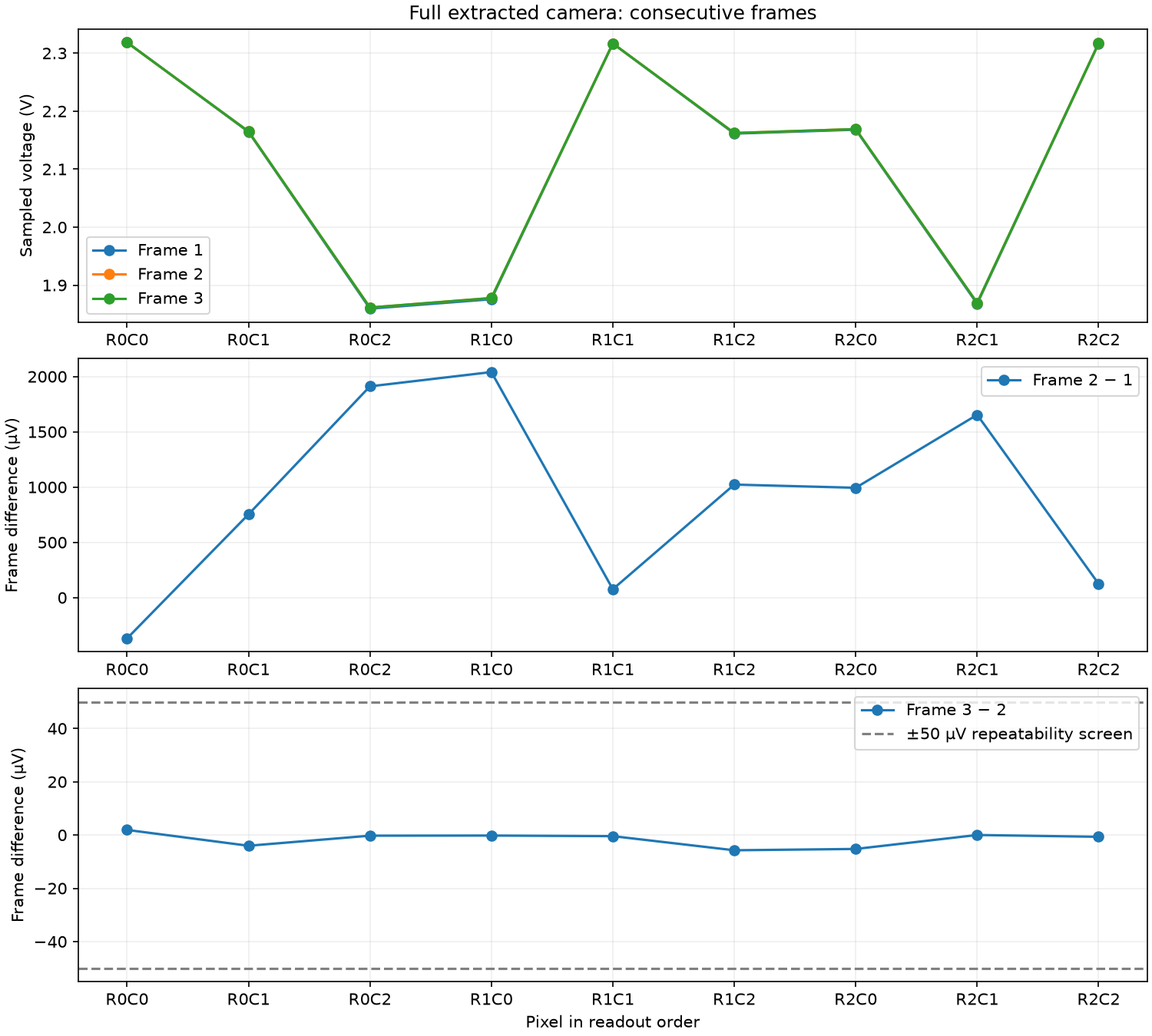
Previous nominal result: Three full-camera frames complete with 27 samples. Frame-two/three drift is 5.733 µV, and matching DC readout references are checked. Results and exact scope.
Standalone rows: All three rows have identical local devices, and all 12 standalone reset tests complete—including pad protection, finite supply and finer-step controls. These earlier isolated tests led into the successful staged/full-frame follow-up. Step-by-step row report.
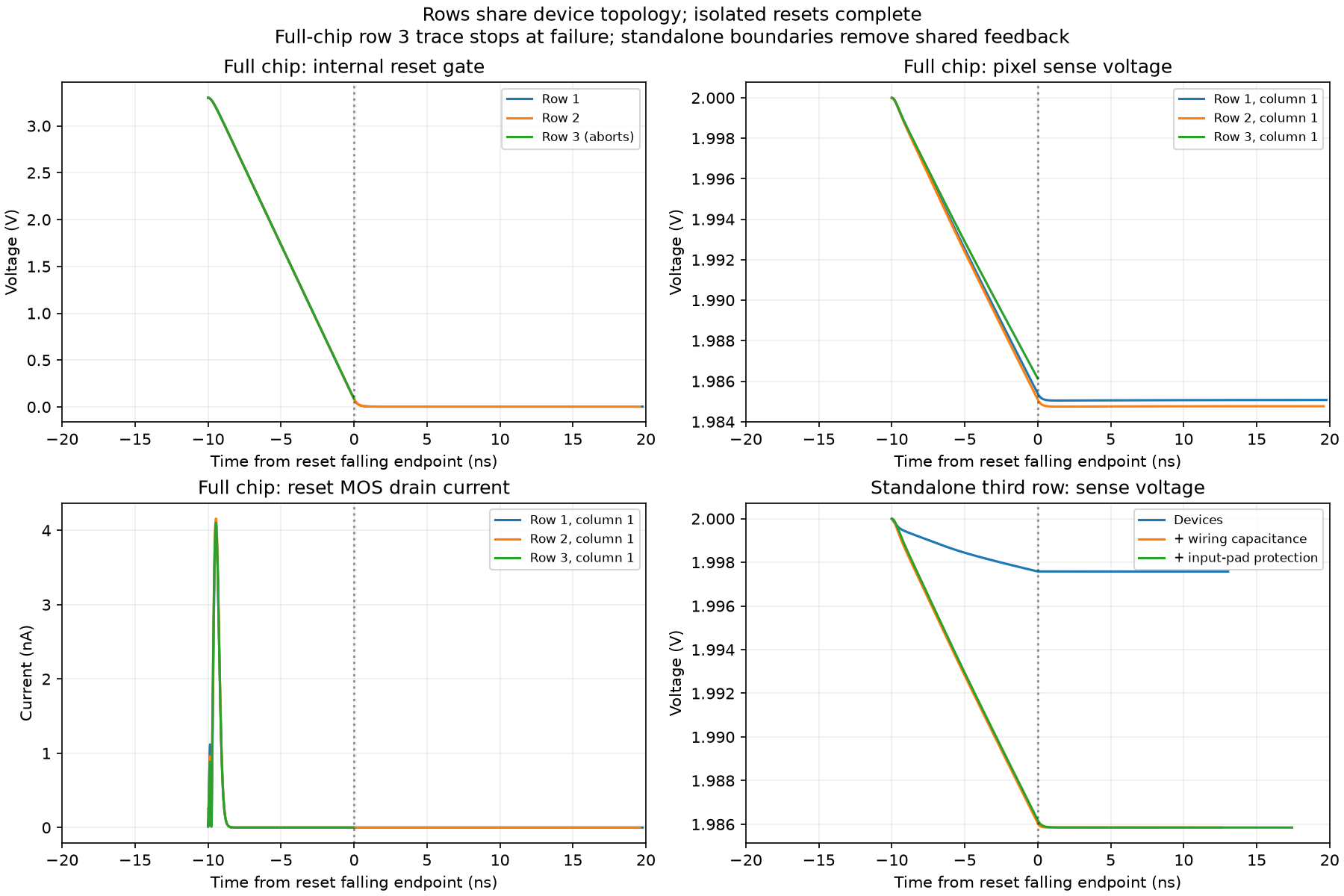
Earlier frame attempt: Explicit solver abort at 3.27002 ms after 21.06 minutes; six pixels retained, third row missing. Results and failure plots. The instrumented rerun reproduces the failure exactly; isolated row tests are described above.
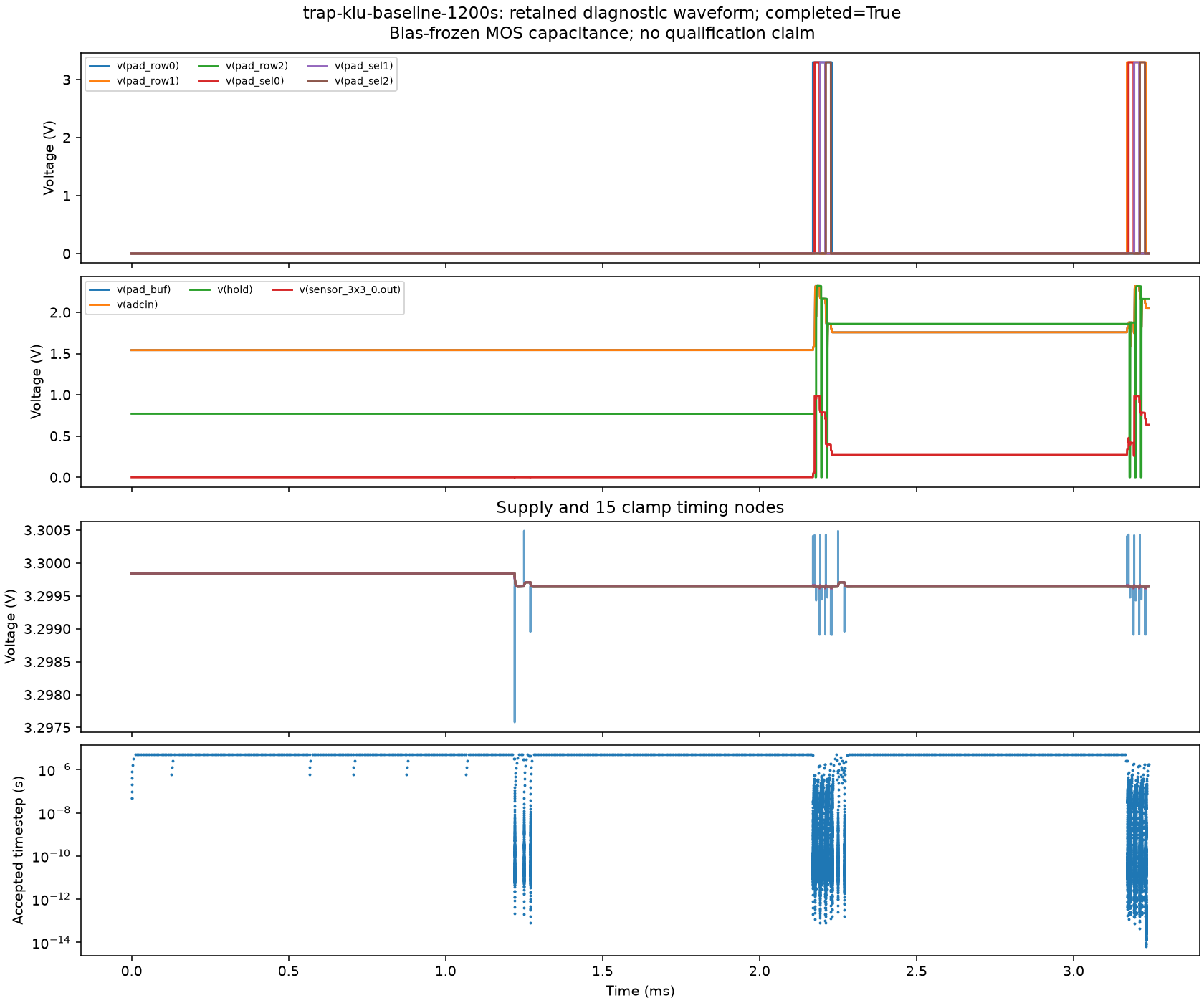
Switching diagnostic: The unchanged candidate crosses the previously reported row-turn-off stall and completes through 3.24 ms. Streaming capture retains six pixel samples; no complete frame or fabrication pass is claimed. Results and plots.
Simulator comparison: matched ngspice 46/47 controls pass, but both extracted stock-model tests fail at startup. Upgrade alone is insufficient; a separate v47 multiplier parser failure has a minimal public issue draft. Results.
Electrical qualification update: Final-chip lumped capacitance and charge-preserving fill reduction are checked. Stricter pad-corner simulations still fail at the clamp load transition; complete-chip electrical qualification is not yet passed. Results and next steps.
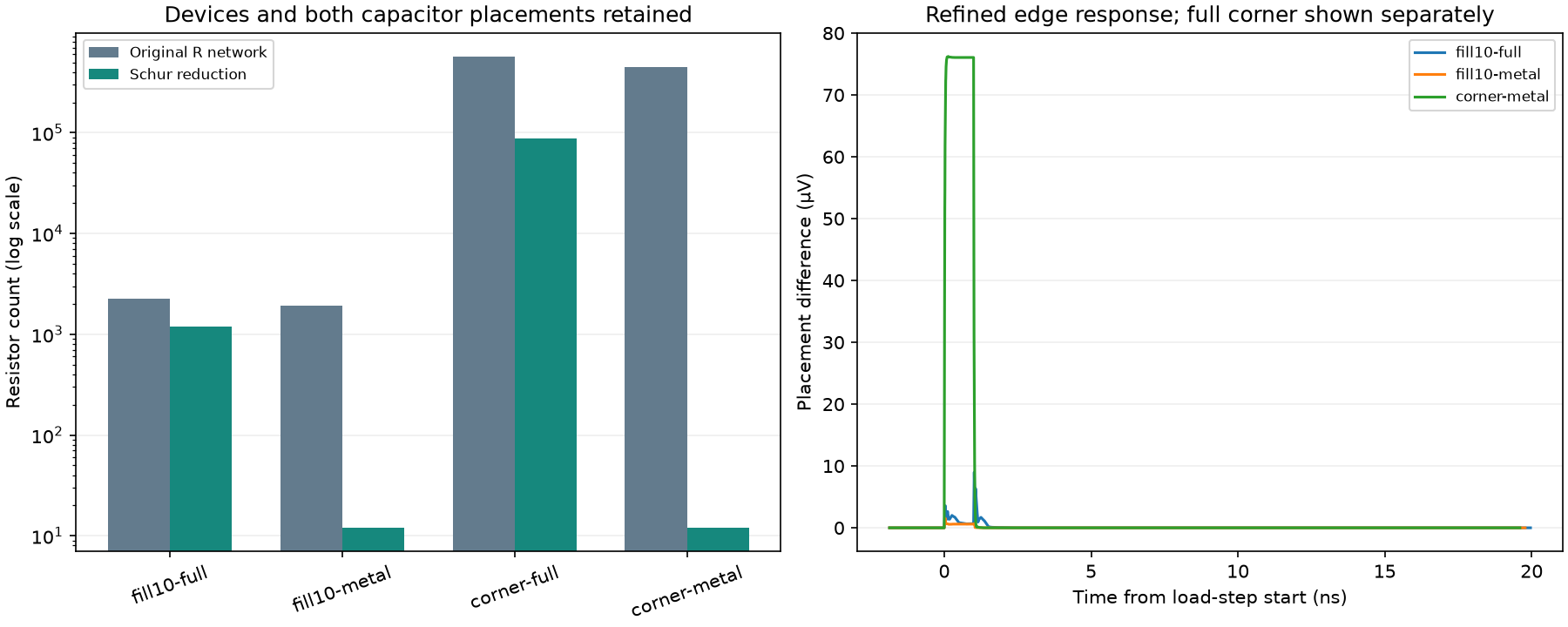
New control-resolution and extracted-clamp results: matched capacitor controls pass the unchanged current limit; the isolated extracted clamp completes and passes 25 ns/tolerance voltage refinement. Both complete-corner capacitance placements now complete at 50 ns. These are diagnostic milestones, not complete-chip qualification. Final-GDS extraction and the remaining electrical gates are open.
KiCad projects and Windows instructions · Illustrated overview · Download review ZIP
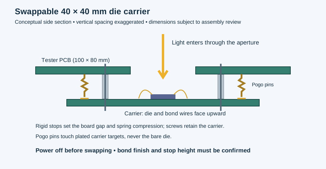
40 × 40 mm removable carrier, underside pogo contacts and an ADS1115 tester. Both PCBs pass the current native DRC and pin/net comparison. Electrical, mechanical and wire-bond reviews remain open; this is not a fabrication release.
Path to a working camera — 19 September 2026: Finish the 3×3, characterize the photodiodes, then scale to 64×64. Carrier/interface and manufacturing planning can proceed alongside the clamp-model review.
First release: 3×3. The core has earlier passing checks; the assembled chip is not fabrication-ready. A new evidence-backed numerical candidate passes isolated-clamp voltage refinement and completes both corner-placement transients; the final-chip electrical tests remain open. The working pad arrangement now has verified routing and central fill; density, antenna, main DRC and device LVS pass. Electrical and manufacturing qualification remain open.
Electrical blocker explained: local clamp-model review. The original failure and subsequent control-resolution findings are documented; the candidate is not yet an accepted full-chip fix. No external expert has yet reviewed the packet.
Completion plan · Pins and board interface · Unsent expert-review package · Manufacturing questions
Historical diagnostic checkpoints below retain their original scope and limitations.
MOS-capacitor diagnosis (2026-09-19 01:49 PDT): 24/24 simple capacitor transients complete; 0/4 initial isolated-clamp transients complete. Integration follow-up: 1/2 complete; refinement: 0/2 pass. Report and plots.
Latest simulation check (2026-09-19 01:32 PDT): DC/AC interface comparison: NOT VERIFIED. Full-corner ramp/load transients: NOT VERIFIED. Details.
An open monochrome image-sensor experiment using GF180MCU, Xschem, ngspice, gdsfactory, Magic, KLayout, and Netgen.
Project checkpoint: 18 September 2026 · Changelog · Dated next steps and handoff · Engineering notebook
The active target is nine pixels with external timing and an external ADC. The core layout and earlier electrical checks exist; functional signal-pad routing is implemented in a working candidate; full-chip verification and optical packaging remain open.
Current plan: completion milestones and stop rule · logical pins and board interface · manufacturing questions · simulator review package.
Signal path: light → pixel → column bias/multiplexer → shared buffer → signal pad → board ADC → controller. The earlier power-only vehicle is superseded by the separate routed working-layout checkpoint below.
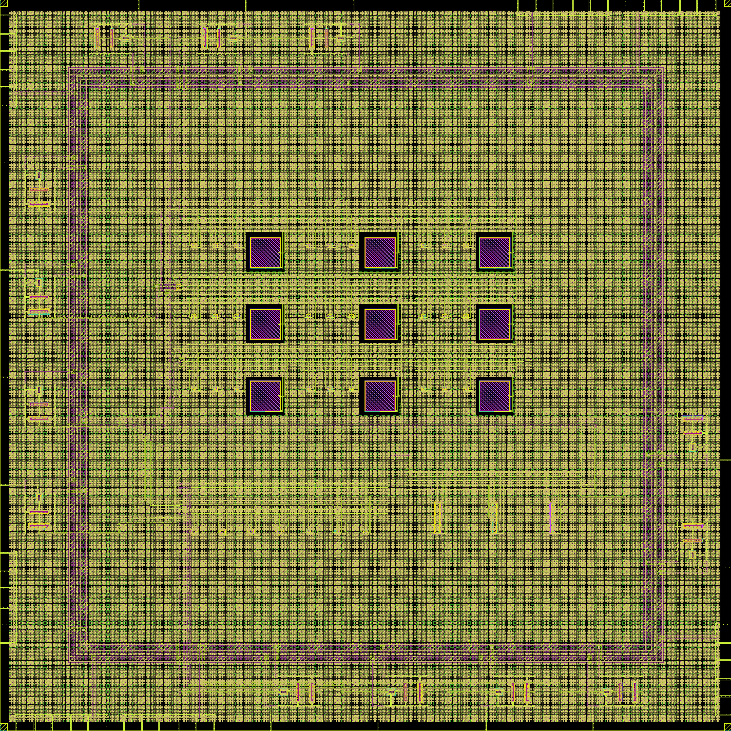
Regenerated central fill with all nine optical keepouts preserved. Density/antenna and main KLayout DRC report zero violations; device LVS matches uniquely; all 4,566 connectivity checks pass. Verification report · HTML overview. Full-chip electrical qualification and run-specific manufacturing checks remain open.
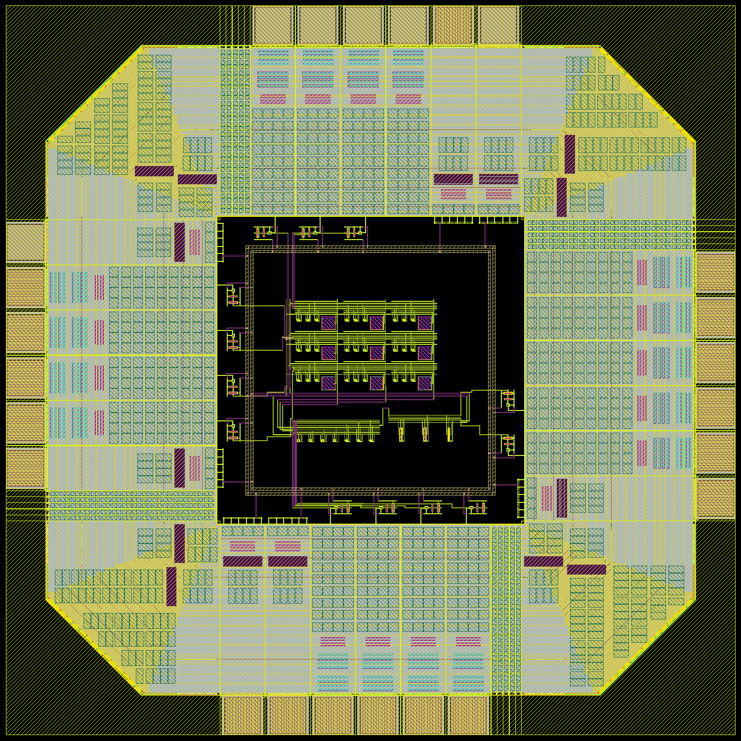
13 functional signal paths routed through local protection; seven supply/return pads connected. Metal connectivity: 4566 checks, PASS. Main KLayout DRC: 0 markers. Magic DRC: 0. Device LVS unique match: True. The four diagnostic signal paths remain disconnected. Final fill, manufacturing and electrical sign-off remain open. Verification report.
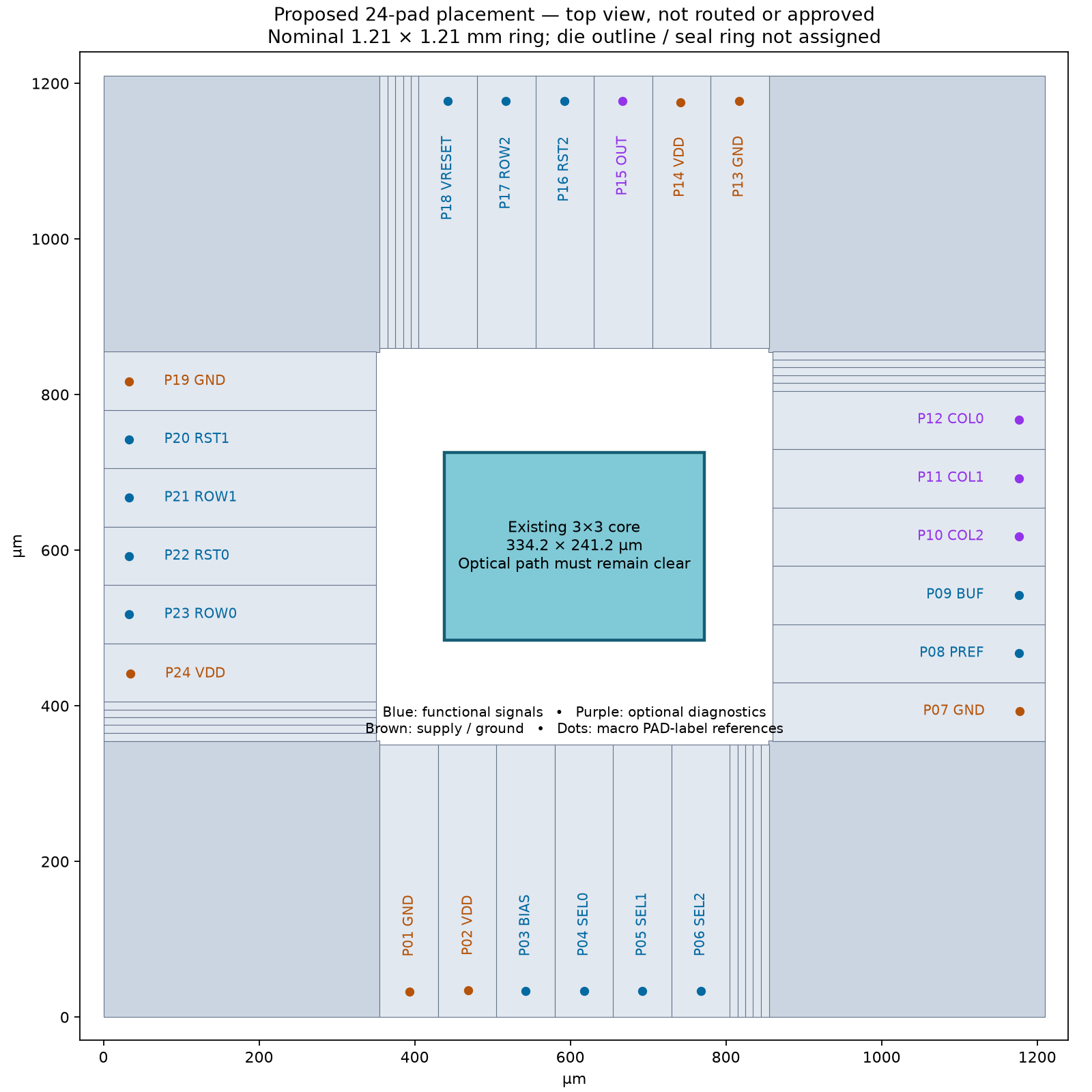
Original placement-only concept, now approved for local implementation: 19 core nets, 24 pads. See the newer routed checkpoint above. Die outline and optical packaging remain open. Pad table and review gates · Coordinate CSV.
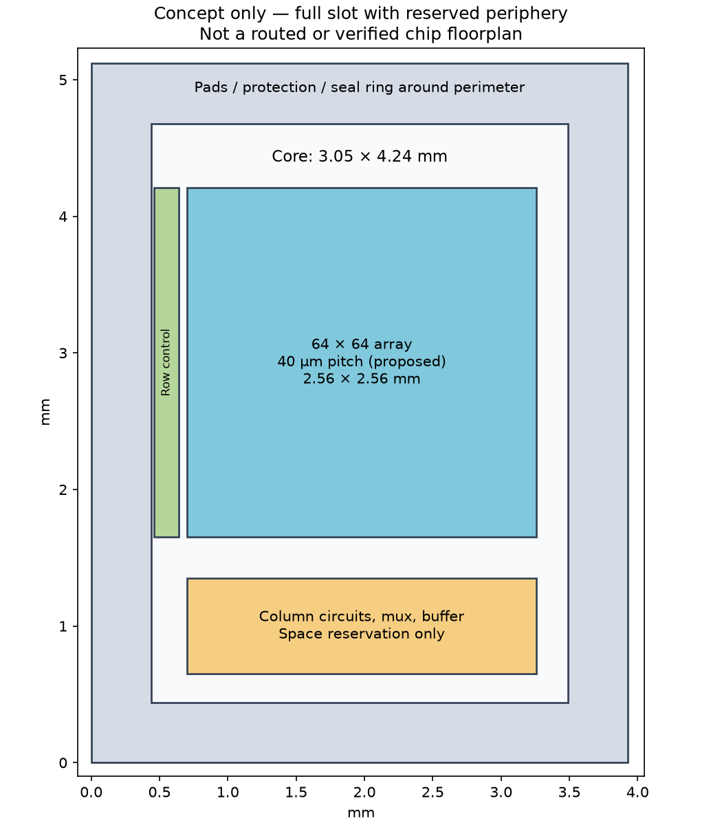
This is a future concept, not part of the first release or a routed and verified chip. Earlier area estimates do not establish manufacturing or packaging acceptance.
Four resistor reductions pass numerical and DC checks. Full corner: 571,551 → 87,748 resistors; metal-only corner: 451,892 → 12. Placement sensitivity is now measured in coupon fixtures, with numerical and startup limits retained. Results.
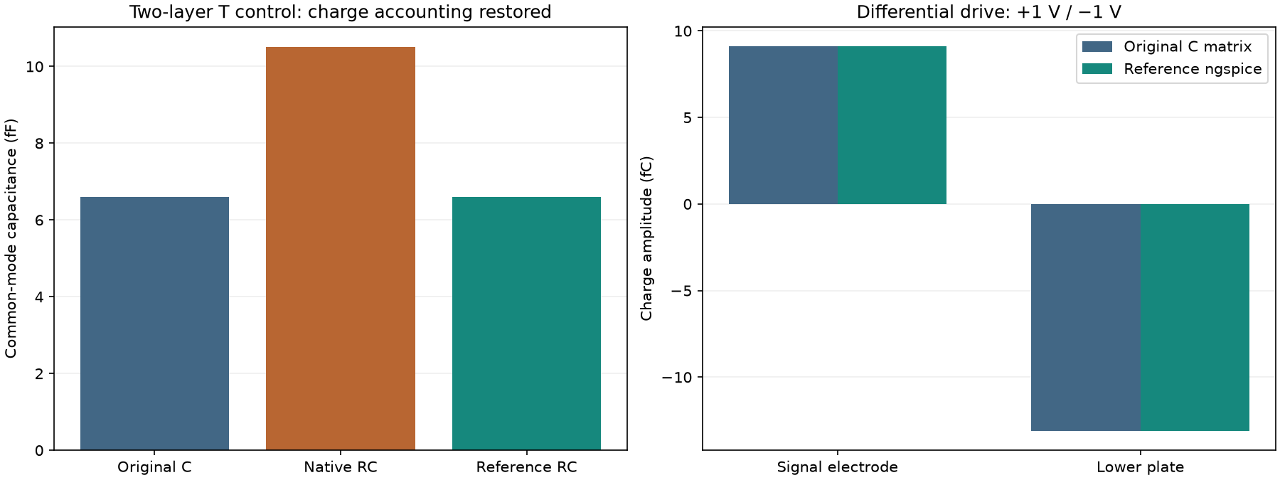
The first finished chip will be the 3×3 demonstrator. Eight reference models preserve the original capacitance matrix; 16 independent charge checks pass. Capacitance placement and integrated transient qualification remain open. Evidence · Completion plan.
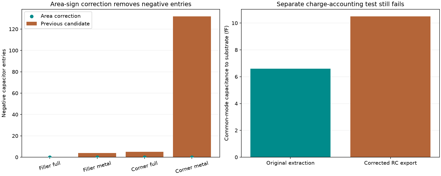
The area-sign patch removes negative capacitances in all four ring coupons; LVS and DC checks pass. A separate charge-accounting error remains, confirmed with small ngspice controls. Evidence · Completion plan.
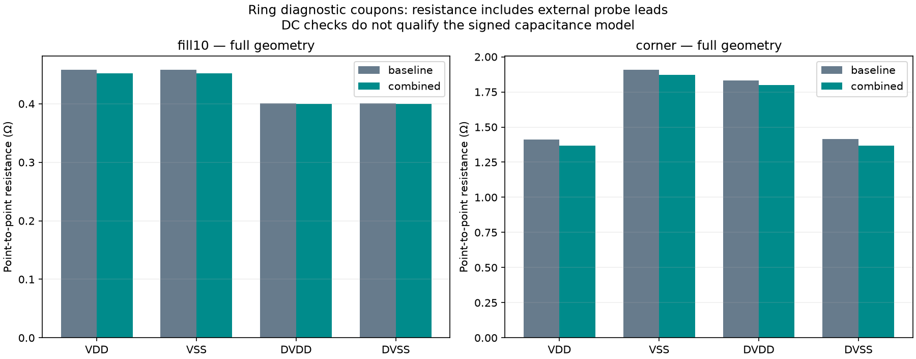
Four device LVS checks and 32 DC rail solves pass with matched ring coupons. The combined extraction candidate still produces negative-energy capacitance nodes in the corner; transient acceptance remains blocked. Audit and next work.
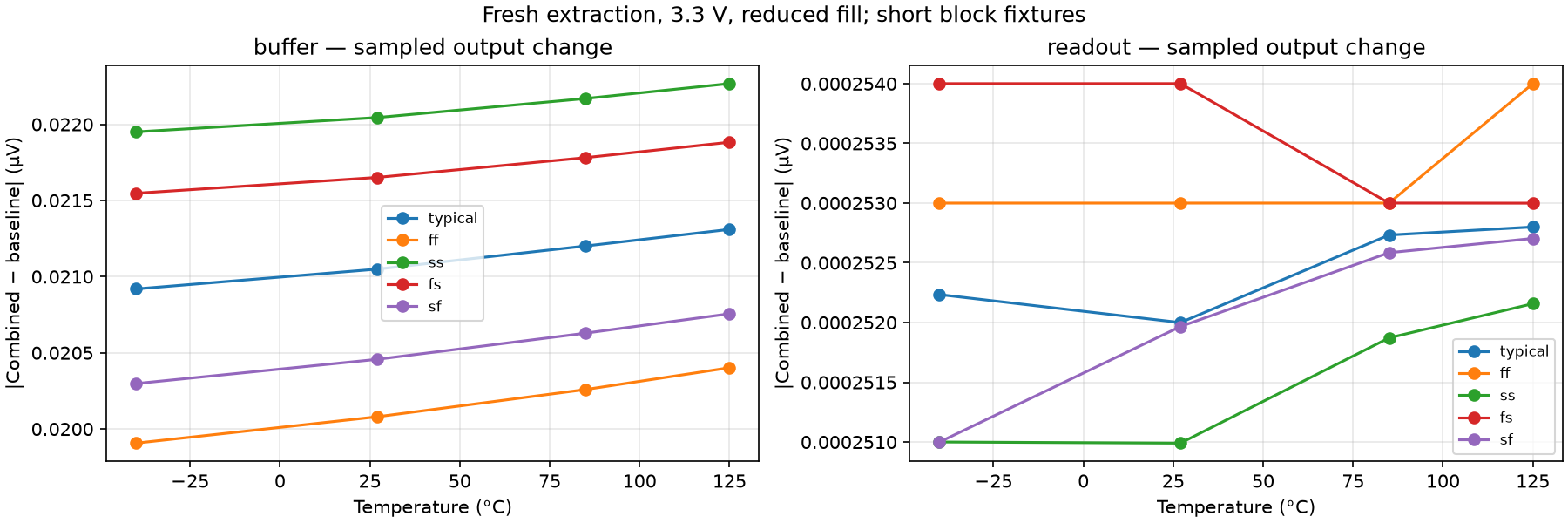
Four LVS comparisons and 80 block transients pass across five process corners and −40 to 125 °C. Largest sampled baseline/candidate difference: 0.02227 µV. Diagnostic candidate only; full-ring extraction remains open. Report.
The two-layer discrepancy comes from construction-time triangle reductions in the tested Magic version. Removing six half-milliohm additions restores the unreduced network result: 0.093837 Ω for the 300-via control, versus 0.118443 Ω originally.
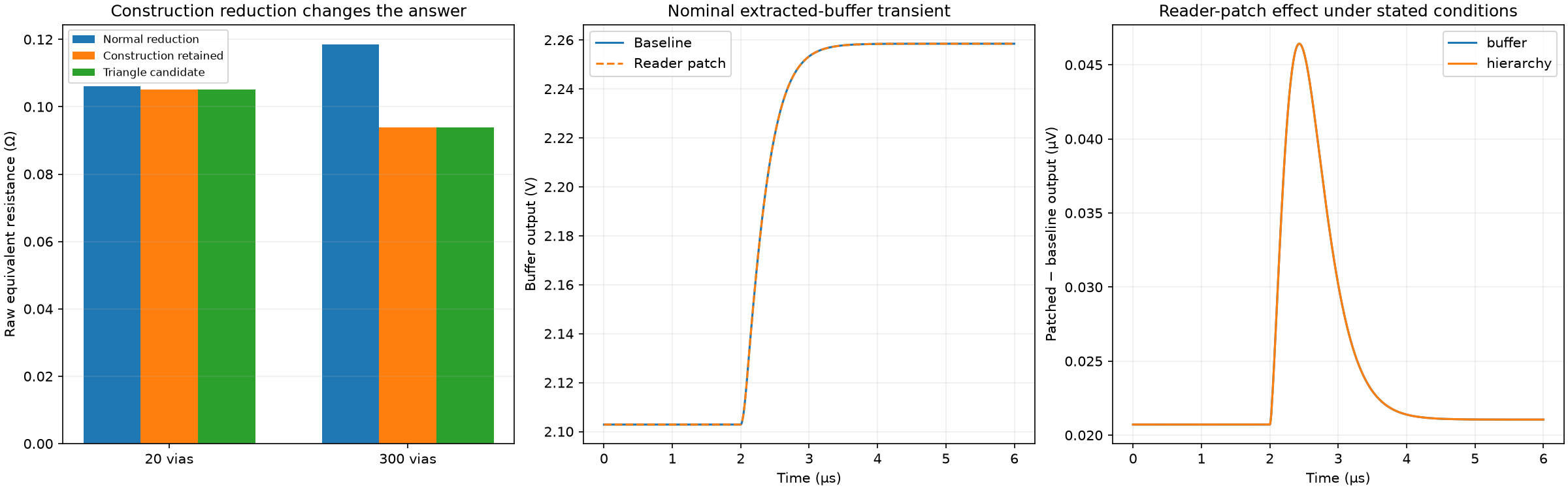
The separate reader patch preserves devices, capacitances and hierarchy. Four nominal buffer/hierarchy transients pass using the existing verified floating-fill reduction; direct raw-network attempts timed out. The patches remain diagnostic, with combined qualification still ahead.
Results, source references and reproduction · Notebook
A controlled one-line reader patch removes the 0.0005 Ω per-resistor export increment in all five test stacks. An unmodified build with the same configuration reproduces the installed behavior, and independent ngspice checks pass. The full-stack diagnostic export now matches raw resistance: 0.0891035 Ω instead of 0.0990837 Ω.
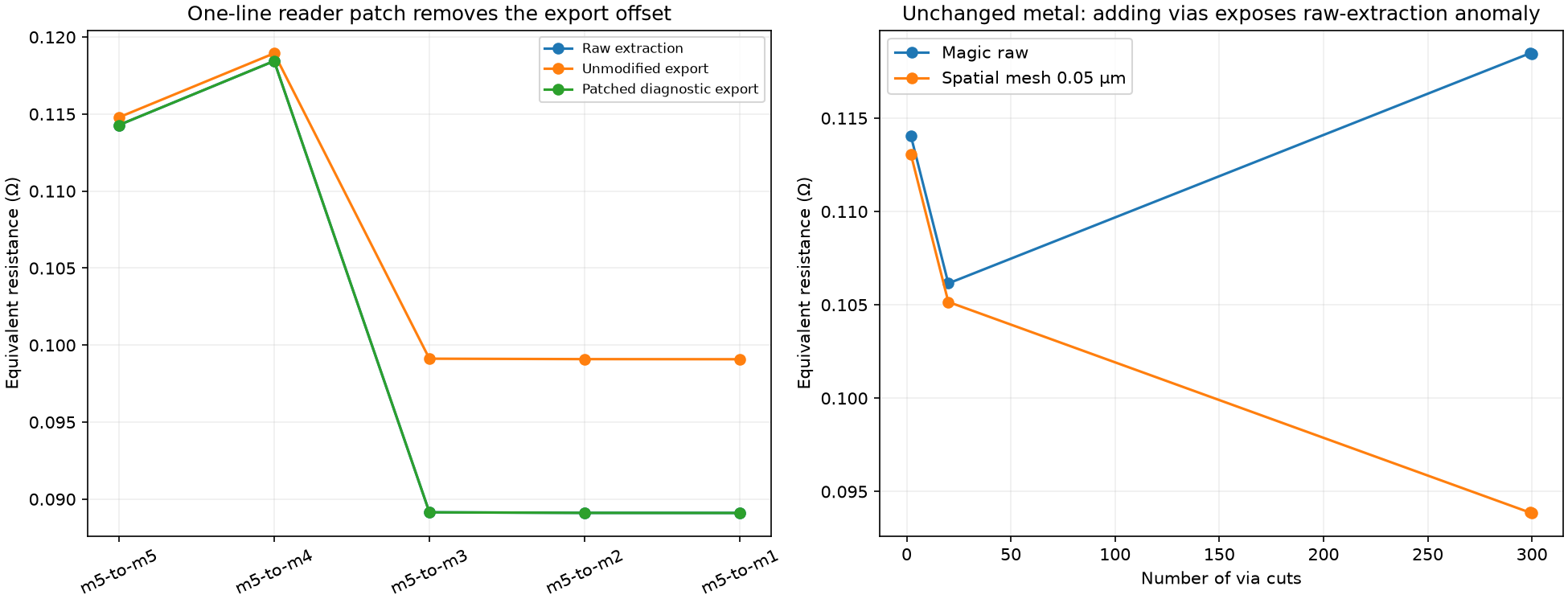
The two-layer problem remains in raw extraction: adding vias to unchanged metal raises Magic resistance while the spatial model decreases. The patch remains diagnostic; full RC qualification is open.
Evidence, source reference and reproduction · Notebook
Measuring the M5 rail through its full-width ends gives 0.1142857 Ω, matching the analytic value 0.04 × 20 / 7 and raw Magic extraction. This removes the large narrow-probe discrepancy in the M5 control. With three or more layers, raw Magic and the spatial model agree within 0.013%. SPICE export adds about 11.2% to this low-resistance network; that conversion and the exceptional two-layer Magic result remain under investigation.
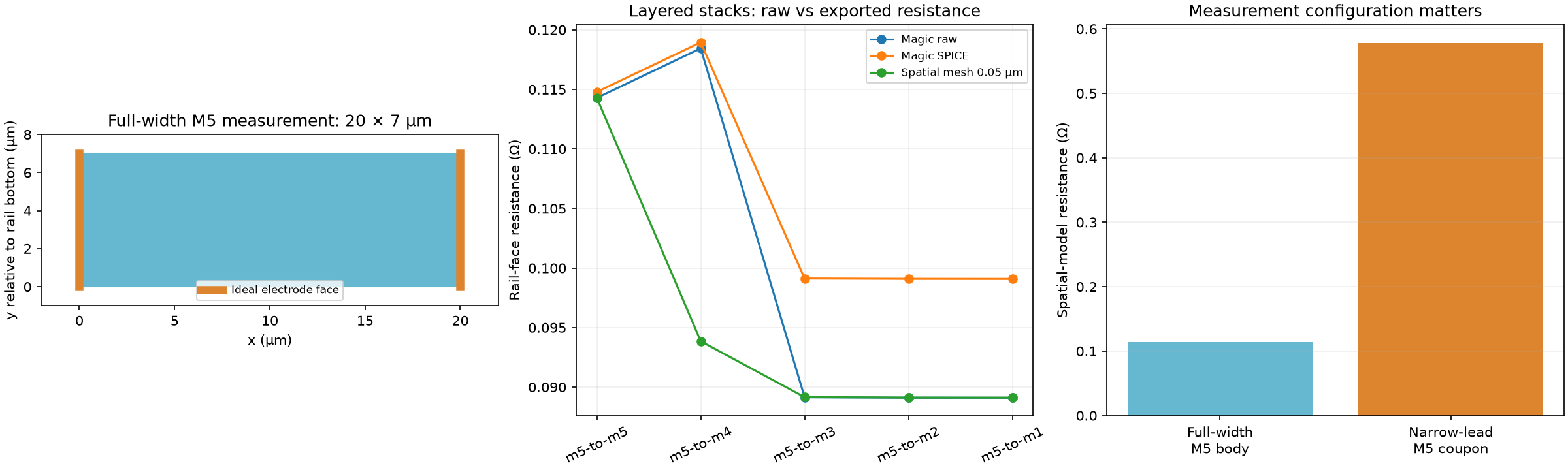
Results and reproduction · Living notebook
The disagreement already exists in the actual M5 rail before vias are added. Its narrow measurement leads widen into the rail: the spatial mesh settles near 0.5777 Ω, while Magic gives 0.5143 Ω, matching a simple series-strip approximation. Adding lower layers reduces the mesh resistance; one Magic stage instead increases, so absolute extraction accuracy remains open.
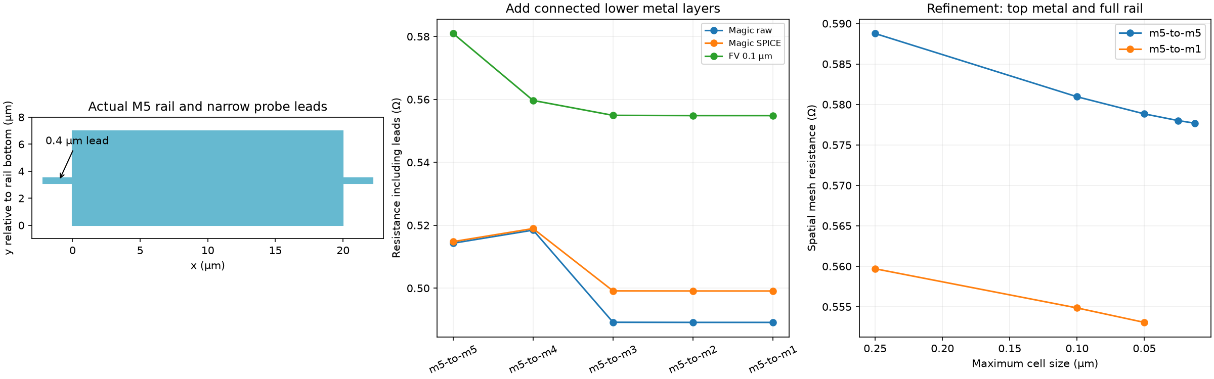
All five Magic exports pass independent ngspice checks. Results, corrected extraction syntax and next experiment · Notebook
Matching terminal positions closes the straight-strip resistance difference: 0.192 Ω in the analytic, mesh and raw Magic models. Small bend/via controls now quantify the remaining differences. The real filler still differs by approximately 12–18% under the matched-plane hypothesis, so full RC qualification remains open.
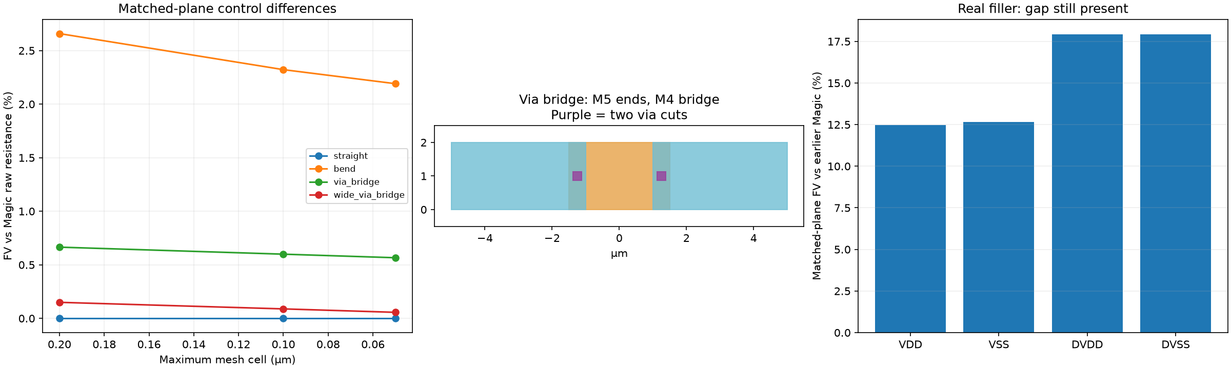
Results and reproducible experiments · Living notebook
Corrected ideal-electrode treatment now passes four analytic M5 strip controls at two mesh sizes. The corrected two-filler model passes DC stitching, including an independent ngspice check at 1 µm. Absolute resistance remains unresolved: the fine mesh is still about 10–15% above the earlier Magic control.
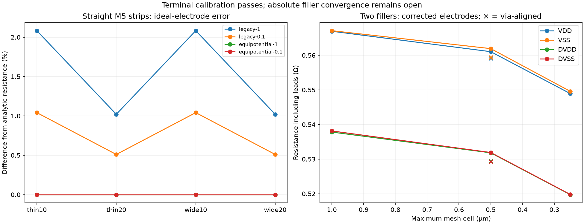
Results, extraction selection pitfalls and reproduction · Updated notebook
A conductor-only DC benchmark now preserves all 81 metal intervals between two fillers. The stitched and combined models agree below the 1e-8 relative screen across four meshes; the exported two-part SPICE model passes an independent ngspice check at the 1 µm mesh.
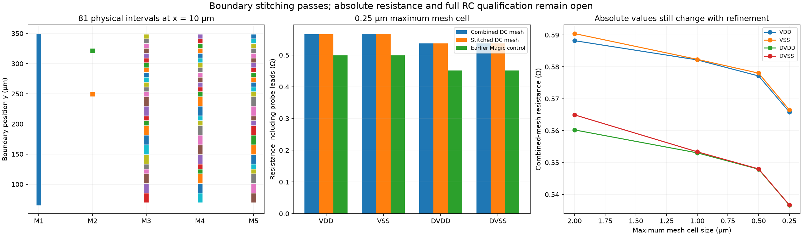
This is not yet a stitched Magic RC model. Absolute resistance remains mesh-sensitive and differs from the earlier Magic extraction. The finer simulator attempt timed out; matrix checks are recorded separately. Method and remaining work · HTML results.
Four small coupons now extract in under 29 seconds: one filler, two fillers, a corner, and a corner joined to a filler. Device LVS and the documented DC terminal/current-balance checks pass. The corner checks use our tied analog supply domain.
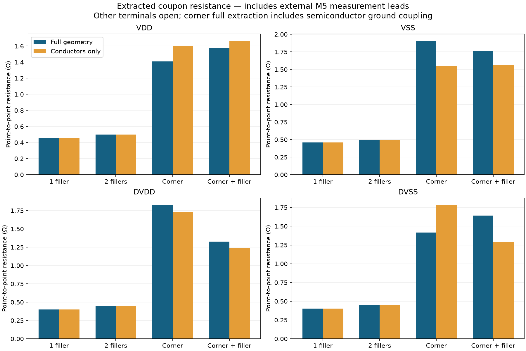
These measurements include external probe leads. Corner substrate coupling, negative capacitance entries, and consistent multiport boundaries still need resolution before full-ring camera simulation. Experiment notes · HTML comparison.
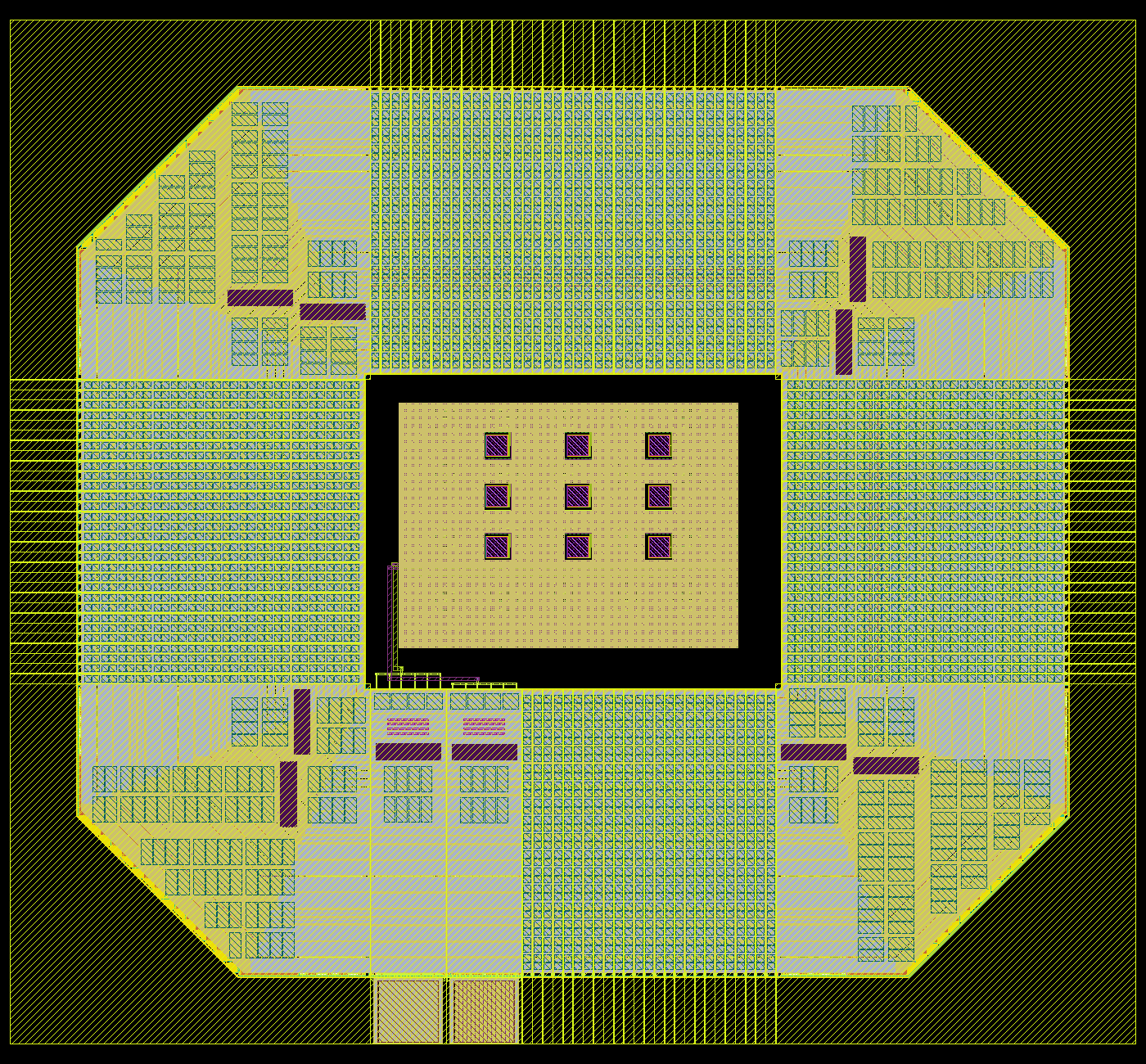
The unchanged 3×3 sensor now sits inside a 1.110 × 1.010 mm foundry-macro supply ring, with routed power and ground. Ring device LVS matches uniquely; configured KLayout DRC reports zero violations on the ring and assembly, and 10,948 physical continuity probes pass.
Extracted connecting-wire resistance is 5.147 Ω on VDD and 7.195 Ω on ground. Nominal and hot load tests pass the 1% rail screen using foundry schematic ring models plus those wire parasitics. Full-ring distributed RC extraction remains unfinished. Signal pads, complete camera simulation with ring RC, and fabrication qualification remain to be done.
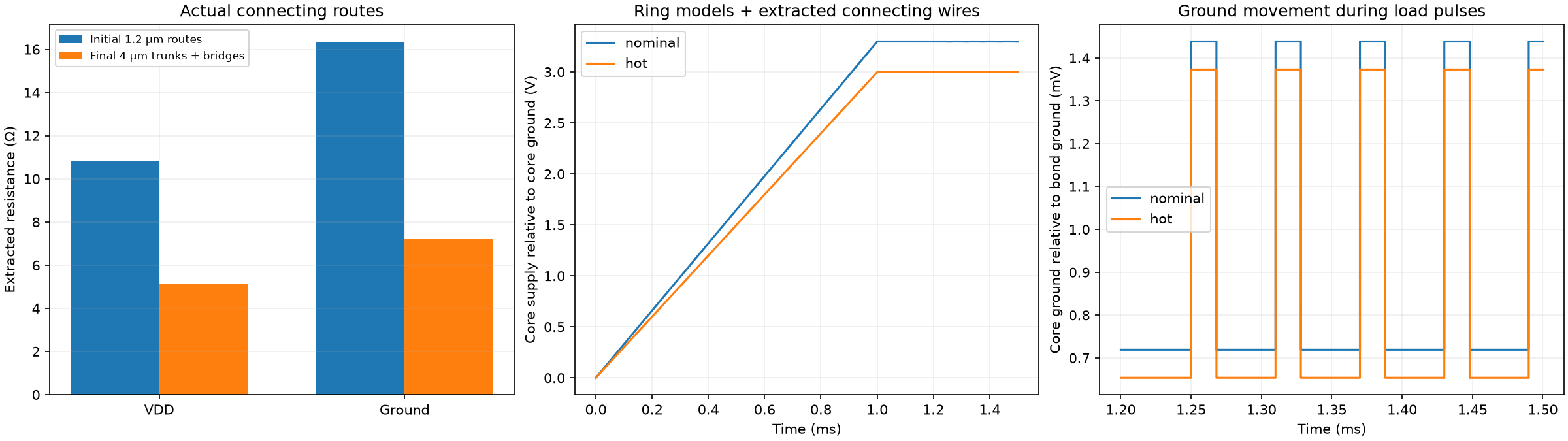
The plot uses ring schematic devices plus extracted connecting wires. It does not include full-ring metal RC. Ring DRC uses all,-antenna,-density,-cup; these results are development checks, not complete die signoff.
Results and plots in the running notebook · Reproduction and limitations
The extracted 3×3 camera and foundry supply clamps are now tested with an assumed board RLC supply and local decoupling. See the running notebook for nominal/hot results, a weak-supply sensitivity case, and numerical checks. Reproduction instructions identify the model assumptions and remaining regulator/package/pad-ring work.
The unchanged analog-pad interface has zero main, density and antenna DRC markers using wafer.space's published rule selection. That selection excludes CUP; the earlier unfiltered report retains its 87 CUP.3 findings. This is a coupon-level check, not a full die submission precheck.
A foundry VDD/VSS clamp pair is now modeled on the 3.3 V analog supply. Across 324 DC cases, modeled pair leakage is 0.146 nA nominal, 76.19 nA maximum. Fast ramps activate the clamps strongly. A 1 ms soft-start plus 200 µs reset hold is the current candidate: all 18 finite-source follow-up cases settled, including six 1 ms cases. High-voltage MOS models remain typical; this is not complete ESD or transistor-corner qualification.
The full three-frame camera-plus-clamp simulation is now verified at nominal and hot conditions. All 27 samples per run pass, with worst sampling error 0.221 mV. The direct connection uses a 1 pA absolute-current tolerance and a 1200 s watchdog; independent strict-tolerance and finer-step checks corroborate the results. See the convergence report and reproduction instructions.
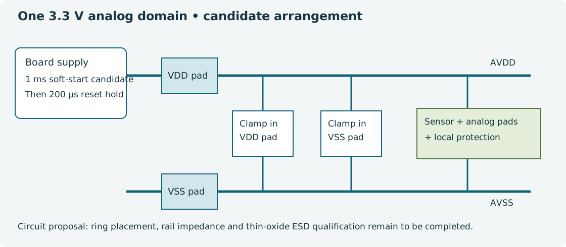
See the running notebook and reproduction notes for comparison plots, numerical failures and follow-ups, exact rule selection, and qualification limits. This earlier simulation uses a supply-pad pair. The physical ring above adds corner clamps and filler decoupling; its full RC camera simulation and stress qualification remain open.
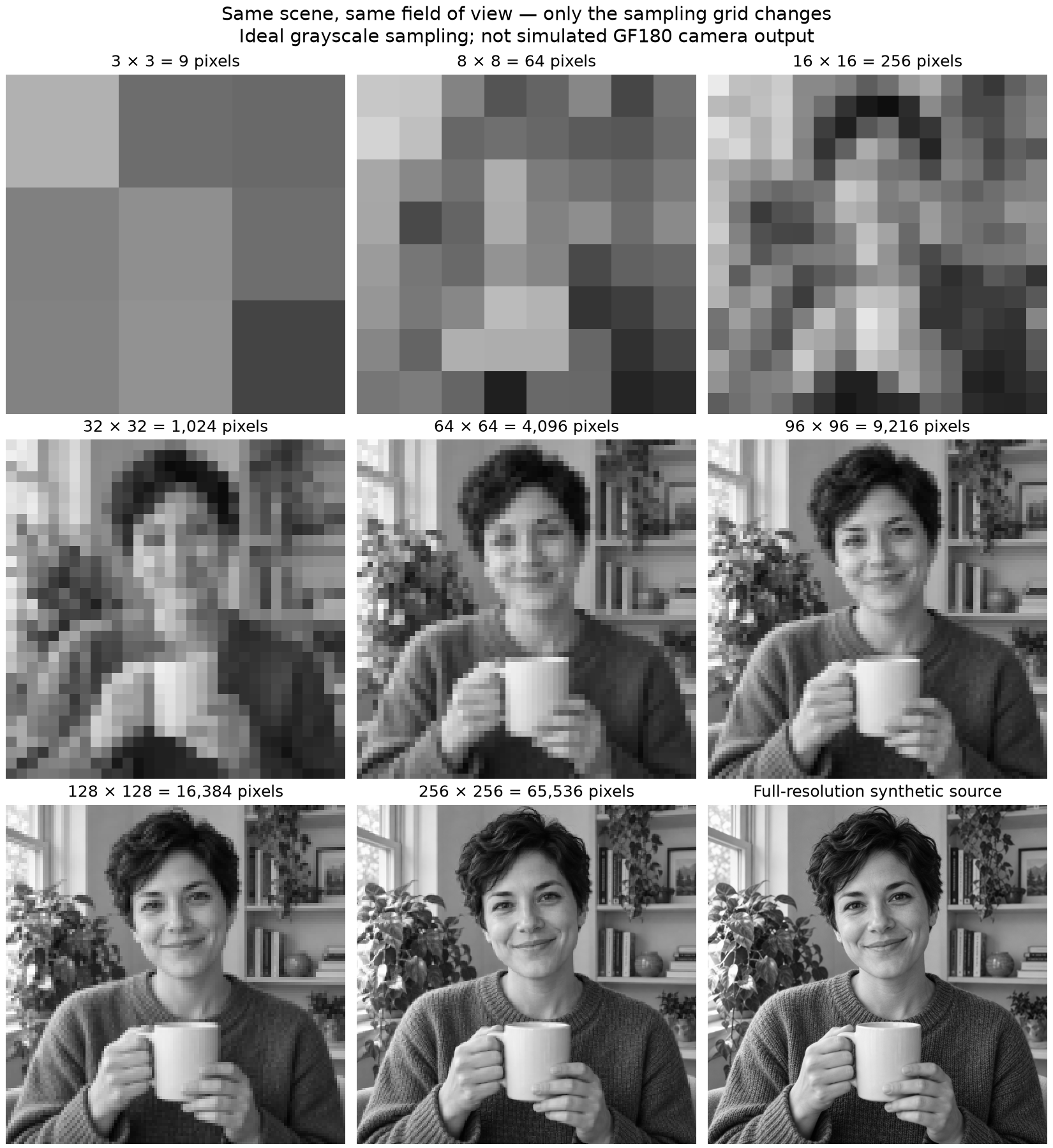
The same synthetic scene is sampled at each resolution with a fixed field of view. This illustrates ideal sampling, not predicted GF180 image quality; noise, optics and detector efficiency are not modeled, and higher resolutions shown here are not claims of fitting this die.
The HTML notebook includes an interactive resolution
slider, manufacturing and packaging research, and the full design history.
Clone or download the repository and open docs/overview.html in a browser to use the slider offline. Keep the adjacent docs/assets/ folder for the newer layout and result images. The images above provide the README preview.
A connected 3×3 physical array, matching hierarchical Xschem schematic, row-scan simulation, zero Magic DRC errors, zero violations from the installed full GF180MCUD KLayout DRC deck, and unique Netgen LVS matches. The checked array contains 27 MOSFETs and nine physical diodes. These are local core checks, not a completed camera or manufacturing signoff.
docs/assets/ beside it.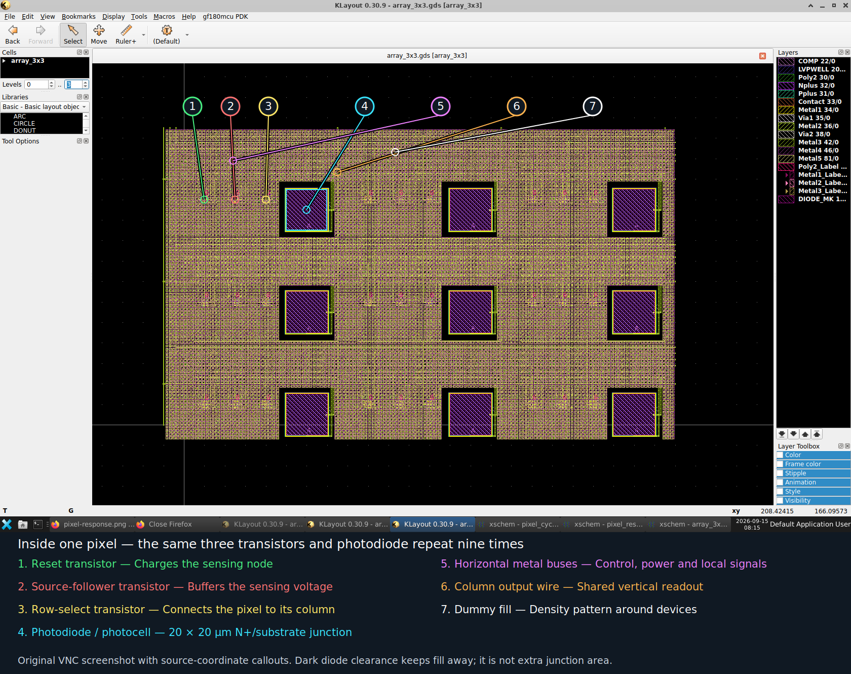
The larger variant has nine 20 × 20 µm photodiode junctions at an 80 × 50 µm pixel pitch. Labels identify one representative pixel; its three transistors and photodiode repeat nine times. Callouts use source coordinates over the original VNC screenshot. Open the scalable image.
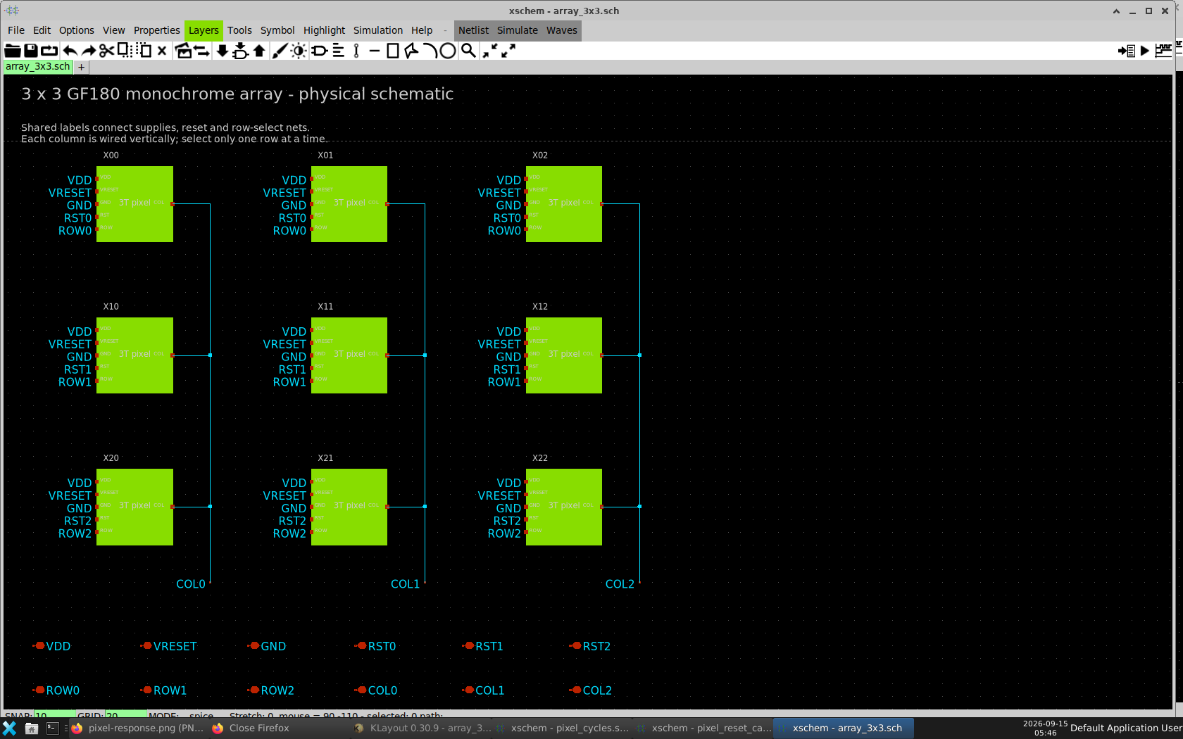
Each block contains a reset transistor, source follower, row-select transistor and photodiode. The rows share reset/select controls and the three columns provide separate outputs. This hierarchy is shared by all three diode-size variants. Open the Xschem source.
No host .venv is required. The scripts use the existing IIC-OSIC-TOOLS Docker
image pinned in scripts/run-tools.sh, which contains gdsfactory 9.44.0 and
all currently required EDA tools. Set IIC_OSIC_IMAGE to override the image.
The old prototype's gf180mcu Python package is not installed; the new layout
imports checked PDK-generated primitive GDS into gdsfactory instead.
With Docker Desktop/WSL integration available, run from this directory:
python3 scripts/make-array-schematics.py
bash scripts/verify-array.sh
bash scripts/run-tools.sh python3 scripts/build-overview.py
The existing report also incorporates prior single-pixel experiments. Their
reproduction commands are listed in docs/README.md; on a clean checkout,
regenerate those baseline waveforms before rebuilding the complete notebook.
Results include build/array_3x3.gds, reports under build/array-check/, and
machine-readable measurements under simulations/. Share the docs/ directory together so the notebook and its linked assets open offline.
The 20 µm 3×3 array now has extracted resistance and capacitance models, with schematic, C-only and RC scan comparisons. See the HTML notebook and reproduction method.
The latest candidate uses a 40 µA buffer reference and an all-row startup reset. See the updated notebook and diagnostic/reproduction notes. The standalone three-PMOS buffer layout passes Magic DRC, KLayout DRC and Netgen LVS.
The buffer now has an extracted RC model connected to the separately extracted array and readout. See the latest notebook section and reproduction notes. This earlier experiment used ideal inter-block wiring; the connected layout below supersedes that geometry.
The pixel array, column bias/multiplexer and output buffer now share physical signal, supply and ground routes. The filled layout passes Magic DRC, KLayout DRC and Netgen LVS (37 MOS devices and nine photodiodes).
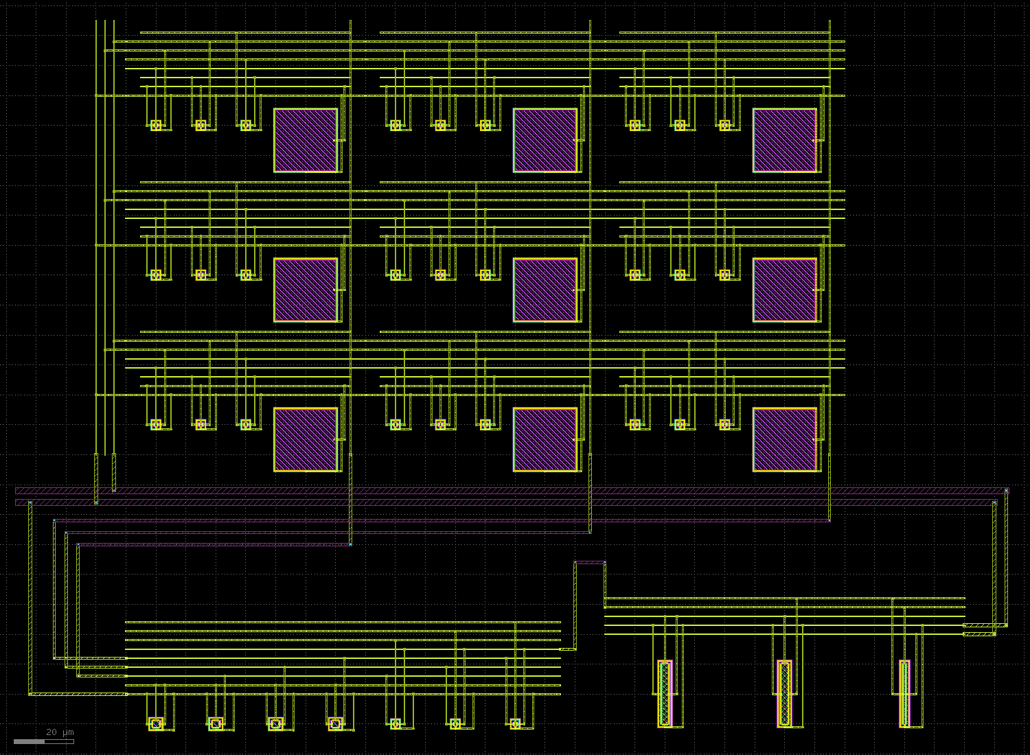
See the connected-layout notebook and reproduction and extraction notes. This is a test core without pads/ESD or physical reference/control generators.
The connected-layout process/temperature matrix extends the initial three checks to 24 conditions. See the scope and reproduction instructions. All 24 RC cases pass the 0.5 mV sampling screen; the worst error is 0.207 mV. This uses fixed nominal wire R/C, ideal reference currents and the generic ADC load.
Two external resistors now replace the ideal current sources in a separate simulation checkpoint: 5.1 MΩ from VDD to BIAS and 49.9 kΩ from PREF to ground, feeding the existing on-chip mirrors. All 84 DC cases converge and all 18 selected startup/imaging cases pass; worst sampling error is 0.216 mV.
See the startup plots and comparison table, component and scope notes, and Xschem interface. This is a board-bias candidate; pad/ESD leakage, resistor TC/noise and actual reset-supply generation remain ahead.
The installed GF180 analog pad plus a candidate local protection network passes five selected extracted-core imaging checks with a finite-transition ADC load: worst HOLD error 0.217 mV against the 0.5 mV screen. Both candidates converge across 84 matched DC cases each; the secondary network changes core reference currents by less than 0.18%.
See the pad evaluation and plots and reproduction/evidence notes. The original ideal-switch secondary-protection runs fail numerically and are preserved. These are functional model results; pad layout, thin-oxide ESD protection and package qualification remain outstanding. The core GDS is unchanged.
A routed local protection cell now passes Magic DRC, the full installed KLayout DRC deck and unique Netgen LVS. Its physical poly resistor is 149 Ω nominal; five selected imaging checks with local extracted capacitance pass, with a worst sampling error of 0.221 mV.
The combined single-pad wrapper matches LVS and is Magic-clean. KLayout reports 87 CUP.3 findings, identical to the untouched library pad, in the unfiltered deck. The later coupon checks described above use the published selection excluding CUP. Neither result establishes ESD qualification or complete-die readiness.
See the layout views and results and reproduction and verification scope.
| Qty | Value | Footprint | References |
|---|---|---|---|
| 24 | 0906-0-15-20-76-14-11-0 | OIS:Pogo_0906_0 | P1, P2, P10, P11, P12, P13, P14, P15, P16, P17, P18, P19, P20, P21, P22, P23 +8 |
| 18 | 100k | OIS:Resistor_SMD_R_0805_2012Metric | R11, R12, R13, R14, R15, R16, R17, R18, R19, R31, R32, R33, R34, R35, R36, R37 +2 |
| 11 | 100 | OIS:Resistor_SMD_R_0805_2012Metric | R1, R2, R3, R4, R5, R6, R7, R8, R9, R24, R25 |
| 4 | 100n | OIS:Capacitor_SMD_C_0805_2012Metric | C1, C2, C3, C5 |
| 3 | 4.7k | OIS:Resistor_SMD_R_0805_2012Metric | R26, R27, R28 |
| 2 | 10n | OIS:Capacitor_SMD_C_0805_2012Metric | C4, C7 |
| 2 | SN74LVC244APW | OIS:Package_SO_TSSOP-20_4.4x6.5mm_P0.65mm | U1, U2 |
| 1 | 10k | OIS:Resistor_SMD_R_0805_2012Metric | R21 |
| 1 | 10u | OIS:Capacitor_SMD_C_0805_2012Metric | C8 |
| 1 | 13k 0.1% | OIS:Resistor_SMD_R_0805_2012Metric | R22 |
| 1 | 1u | OIS:Capacitor_SMD_C_0805_2012Metric | C6 |
| 1 | 20k 0.1% | OIS:Resistor_SMD_R_0805_2012Metric | R23 |
| 1 | 3V3_INPUT_ONLY | OIS:Connector_PinHeader_2.54mm_PinHeader_1x02_P2.54mm_Vertical | J2 |
| 1 | ADS1115IDGSR | OIS:Package_SO_VSSOP-10_3x3mm_P0.5mm | U4 |
| 1 | Alignment round | OIS:Mechanical_5 | H5 |
| 1 | Alignment slot | OIS:Mechanical_6 | H6 |
| 1 | CONTROLLER_TIMING | OIS:Connector_PinHeader_2.54mm_PinHeader_2x10_P2.54mm_Vertical | J1 |
| 1 | FAST_ADC_ANALOG | OIS:Connector_PinHeader_2.54mm_PinHeader_1x03_P2.54mm_Vertical | J4 |
| 1 | I2C_AND_ENABLE | OIS:Connector_PinHeader_2.54mm_PinHeader_1x06_P2.54mm_Vertical | J3 |
| 1 | M3 clearance | OIS:Mechanical_2 | H2 |
| 1 | M3 clearance | OIS:Mechanical_1 | H1 |
| 1 | M3 clearance | OIS:Mechanical_4 | H4 |
| 1 | M3 clearance | OIS:Mechanical_3 | H3 |
| 1 | OPA2320AID | OIS:Package_SO_SOIC-8_3.9x4.9mm_P1.27mm | U3 |

bobasaurus/lumber-plunder-metal-detector
A VLF induction balance metal detector with a wooden body

HearnChristian/polarimeter
4-layer KiCad photodiode polarimeter: low-noise transimpedance front-end (OPA381/OPA320), precision REF3425 reference, LT8609/LP5912 power. Schematic, PCB, gerbers + BOM.

Twisted-Fields/acorn-robot-electronics
PCB hardware designs in KICAD for Acorn, the precision farming rover from Twisted Fields.


codetiger/PowerTiger
Home power monitoring system - Monitoring energy consumption with better granularity


AndreiVladescu/LibrePLC32
The goal of the project is to create a compact, hackable, and well-documented PLC platform for industrial automation experiments, prototyping, education, and open hardware development.
It measures 100 × 80 mm and has 4 copper layers, 1.6 mm thick.
81 parts, built around the SN74LVC244APW, OPA2320AID and ADS1115IDGSR. The full list of its parts is on this page, with links to each part's symbol and footprint where PCBKit's library has them.
From the njcoburn/OPENIMAGESENSOR repository on GitHub, at the commit this page was made from: the board is hardware/carrier/kicad/tester_dock/tester_dock.kicad_pcb and its schematic hardware/carrier/kicad/die_carrier/die_carrier.kicad_sch. PCBKit opens the board in the browser, with nothing to install.
Its repository publishes it under the Apache-2.0 licence: you may reuse it on that licence's terms (keep the author's notice, and for a copyleft licence share your changes alike).