4 layers51.4 × 37.1 mm
Lpc55 carrier
oxidecomputer/hw-lpc55-carrier
Daughterboard which plugs into the Gemini Bringup Board (and gimletlet's carrier-carrier) and provides an LPC55 (root of trust microcontroller)
58 parts1MPL-2.0

 mimok/yast-hw6
Hardware source files of the YAST security token from OTS Security
Tots is an open-source printed circuit board by mimok, from the mimok/yast-hw repository on GitHub, published under the CC-BY-4.0 licence. It is a 2-layer board of 46 × 15.2 mm with 29 parts on 64 nets, routed with 300 tracks and 47 vias.
It is built around the LPC55S28JBD64, TLV75533PDRV and PRTR5V0U2X. Its parts include 13 capacitors, 5 resistors, 3 ICs, 2 connectors and 1 diode. It belongs with the NXP (LPC, Kinetis, i.MX RT) boards of this library.


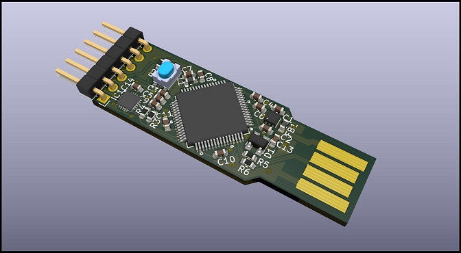
This repository contains the hardware source files of the YAST security token. This security token is intented to be used as a development platform for security applications. It is built around a LPC55Sxx chip and a SE050 secure element both from NXP. This token as the same form factor as the OpenSK token from Google therefore its case can be reused.
YAST is designed to be a development board and therefore should not be used as a daily security token.
On the market there is already a large amount of security tokens. Most of them are based on proprietary designs while some others are open source. On one hand, closed source tokens seem to be based on secure elements while on the other hand, as far as I know, open source tokens are based on standard, not security certified, chips like STM32 chips. This design choice seems to be mainly dictated by concerns about NDA which come with Secure Elements.
From my point of view this is a real problem. I agree some tokens based on secure elements are not exempt from vulnerabilities like the Titan security key from Google. In fact, this token is based on a pretty old secure element A7005 from NXP and therefore things which were secure almost ten years ago are no more secure now. However if a old secure element is now vulnerable (but more than 4 months of work were needed to discover and exploit the vulnerability), old non secure chips are far more vulnerable. For example, it is possible to extract the firmware from an STM32F1 chip using a pure software attack (ok this is not entirely true as an access to the SWD port is needed). This is this chip which is used in the Nitrokey Start key from Nitrokey. While using a secure element is not a "cure-all", using non-secure and non-certified chips for secure application is almost always a bad idea as you relies on a "untrusted" (not certified) chip exectuting an "untrusted" (not certified) code. Here openness is not really a huge advantage as there is very few people around the world which have the required skills needed to perform a valuable security assessment of a security token.
So how a security token can be built using a secure element and still be open source? SE050 security chip from NXP is a pre-programmed secure element embedding a really versatile security applet. All documentation is freely accessible on NXP's website (some documentation requires an account to be accessible) and therefore no NDA is required. The YAST key embeds both a LPC55Sxx chip and the SE050 SE. LPC55Sxx chip can be binded to its SE050 companion using its embedded PUF (Physical Unclonable Function). The resulting hardware comes with both the flexibility and the power of the LPC55 chip and the security of the SE050 secure element which has been certified at level EAL6+ (Hardware and OS) according to the Common Criterias.
YAST token is made of a LPC55Sxx MCU connected to a SE050 coprocessor which acts as a secure cryptographic library. SE050 is designed to prevent both leakage of cryptographic keys and their usage by unauthorized users. In consequence, YAST token is suited for applications which extensively use cryptographic primitives. However, others processing taking place on the LPC55 side do not benefit from SE050 high security level. So before using YAST token for a given application, you should be sure that the following hypothesis are verified:
Concretely, the YAST token can be used to implement application like OpenPGP card (demo application available), FIDO2 protocol (but YAST token does not have any led) or HSM-like applications.
SE050 has some functional limitations which can be circumvented:
At the moment, due to a shortage in LPC55S69 chips, YAST token is based on a LPC55S28 chip which does not implement TrustZone. However these two chips are PIN compatible and token design does not need to be changed if one wants to update the chip.
You can easily build this token yourself. The token is designed using Kicad v5 and you can inspect or modify its design. You will need a PCB with a thickness of at least 2.0mm (best 2.4mm). You can also use a small piece of tape to improve the thickness of your PCB. You should dispense paste on the PCB using a stencil. I use unleaded low temperature Chip Quik SMDLTLFP paste (melting point at 138°C). Placement is not so hard because CMS are not smaller than 0603. The regulator, the SE050 and the LPC55 are the hardest parts to place. Soldering is an easy game if you use a hot plate and a hot-air rework station.
A 6-pin header is available for programming and debugging purpose through LPC55 SWD port. A low cost LPC Link-2 from NXP can be used as a debugging probe. You should update it with the segger firmware to obtain the best performances. USB port can also be used to program the LPC55 chip through the on-chip bootloader:
blhost -u 0x1FC9,0x21 -- flash-image <path_to_hex_file> erase 0
blhost -u 0x1FC9,0x21 -- resetThis token as the same form factor as the OpenSK token from Google therefore its case can be reused. The case can be built using a 3D Printer and PLA plastic.
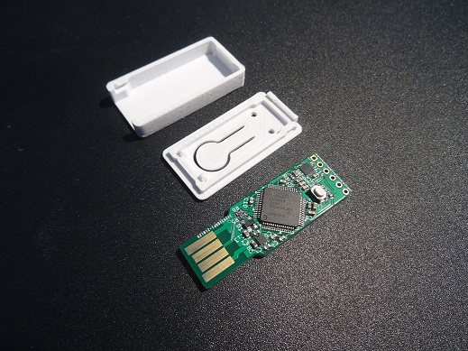
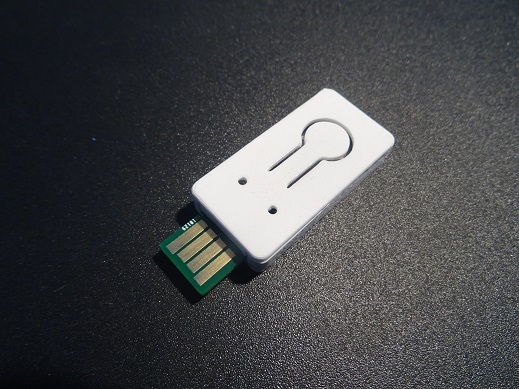
This work is licensed under CC BY-SA 4.0
| Qty | Value | Footprint | References |
|---|---|---|---|
| 7 | 100nF | Capacitor_SMD:C_0603_1608Metric | C4, C5, C6, C8, C10, C11, C14 |
| 2 | 10uF | Capacitor_SMD:C_0603_1608Metric | C7, C9 |
| 2 | 1uF | Capacitor_SMD:C_0603_1608Metric | C1, C2 |
| 2 | 33R | Resistor_SMD:R_0603_1608Metric | R5, R6 |
| 2 | 560R | Resistor_SMD:R_0603_1608Metric | R3, R4 |
| 1 | 10k | Resistor_SMD:R_0603_1608Metric | R2 |
| 1 | 2.2uF | Capacitor_SMD:C_0603_1608Metric | C13 |
| 1 | 221R | Inductor_SMD:L_0603_1608Metric | FB1 |
| 1 | 4.7uH | Inductor_SMD:L_0603_1608Metric | L1 |
| 1 | 47pF | Capacitor_SMD:C_0603_1608Metric | C3 |
| 1 | Conn_01x06 | Connector_PinHeader_2.54mm:PinHeader_1x06_P2.54mm_Horizontal | J2 |
| 1 | LPC55S28JBD64 | tots:LPC55S28JBD64 | U1 |
| 1 | PRTR5V0U2X | Package_TO_SOT_SMD:SOT-143 | D1 |
| 1 | PTS810 SJK 250 SMTR LFS | tots:PTS810SJG250SMTRLFS | SW1 |
| 1 | SE050C1HQ1_Z01SCZ | tots:QFN40P300X300X33-21N-D | IC1 |
| 1 | TLV75533PDRV | Package_SON:WSON-6-1EP_2x2mm_P0.65mm_EP1x1.6mm | U2 |
| 1 | USB HS | tots:usb-PCB | J3 |
The 27 most common of 29 parts.
oxidecomputer/hw-lpc55-carrier
Daughterboard which plugs into the Gemini Bringup Board (and gimletlet's carrier-carrier) and provides an LPC55 (root of trust microcontroller)

dosdude1/2.5-inch-ide-ssd
A custom-designed IDE SSD for use in any machine that utilizies a 2.5" IDE hard disk.

lollokara/HomeKey-ESP32-PCB
HomeKey-ESP32-PCB A miniaturized, wall-mountable HomeKey reader board

teklabsdigital/TekTag
Biosensor for telehealth, patient monitoring, fall detection, dementia geofencing and cardiograms

mikelawrence/esphome-indoor-multi-sensor-hardware
ESPHome Indoor Multi-Sensor hardware. This design supports Radar/PIR Presence, Temperature, Humidity, Pressure, Light, CO2, CO, VOC, NOX and PM sensors.

JeffersonSchostakovich/halowBoards
MM8108-based adapters in different form factors for EU availability of sub-GHz halow 802.11ah hardware - mainly for decentralised networking (Reticulum mesh) and distributed IoT experimentation purposes.


yuanyong2024/IoT-feather
a IoT evb board that based on Quectel BG95 modem and in adafruit feather form factor
It measures 46 × 15.2 mm and has 2 copper layers, 1.6 mm thick.
29 parts, built around the LPC55S28JBD64, TLV75533PDRV and PRTR5V0U2X. The full list of its parts is on this page, with links to each part's symbol and footprint where PCBKit's library has them.
From the mimok/yast-hw repository on GitHub, at the commit this page was made from: the board is tots.kicad_pcb. PCBKit opens the board in the browser, with nothing to install.
Its repository publishes it under the CC-BY-4.0 licence: you may reuse it on that licence's terms (keep the author's notice, and for a copyleft licence share your changes alike).