Skip to the content
2 layers65 × 78 mmBbb adc, the printed circuit board in 3D

The documentation for this workshop mostly consists of youtube screencasts. The screencasts are deliberately fast, if you need them slower then click the video's settings button and choose a slower speed.

Size
65 × 78 mm
Copper layers
2
Thickness
1.6 mm
Parts
100
Nets
33
Pads
225
Tracks, vias
228, 5
Pours
2
Routed
Yes
KiCad
KiCad 4
Created
20 Jul 2015
Updated
18 Feb 2020

Overview

Bbb adc is an open-source printed circuit board by mattvenn, from the mattvenn/kicad repository on GitHub. It is a 2-layer board of 65 × 78 mm with 100 parts on 33 nets, routed with 228 tracks and 5 vias.

It is built around the REF5050ID. Its parts include 7 capacitors, 3 connectors, 2 resistors, 1 IC and 1 diode.

Main components

1

README

breadboard-psu/README.md

KiCad workshop handout

Shortlink to this page: ven.nz/kicad-ws

The documentation for this workshop mostly consists of youtube screencasts. The screencasts are deliberately fast, if you need them slower then click the video's settings button and choose a slower speed.

You are advised to watch the screencasts all the way through before starting, then reference them as needed.

Each screencast has a clickable table of contents. Click the video's 'show more' link to expose it.

The screencasts show the creation of a simple LED board as a way of showing the process. Don't just follow along - you will be making a breadboard power supply to supply either 3.3v or 5v.
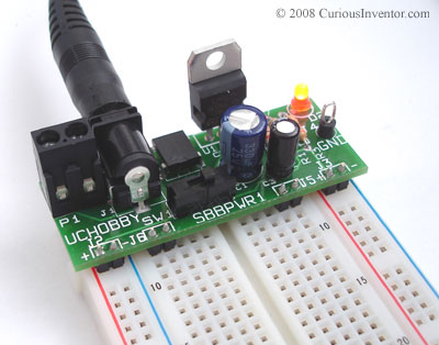
photo

Drawing the Schematic

Watch the schematic creation screencast

Your first task is to produce the schematic below. If you want a 3.3v output use part AP1117D33. If you want 5v then use LM7805CT.
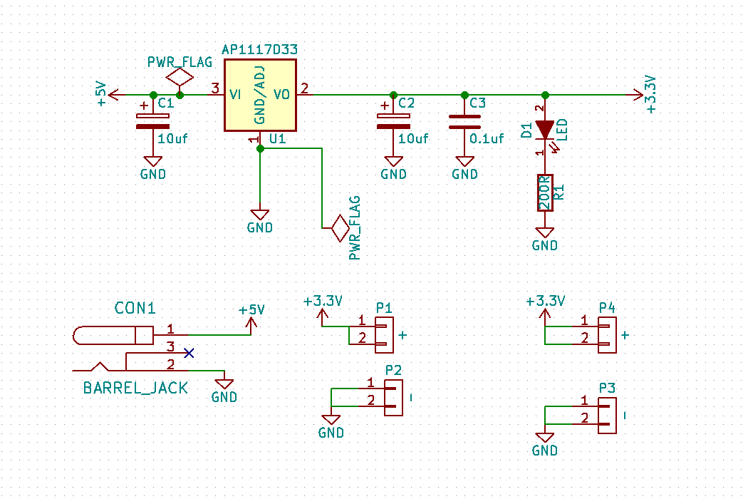
schematic

Tips

  • Don't bother naming components, that will happen automatically when you 'annotate components'
  • The regulator footprint is in the power_integrations library
  • Use the hot keys below!

Hot Keys

  • ? - show hotkeys
  • e - edit component
  • m - move component (without wires)
  • g - drag component (with wires)
  • r - rotate
  • a - add component
  • del - delete component
  • w - start a wire
  • c - copy
  • l - lable a wire (wires with the same label are joined)

Adding a library

The barrel jack's PCB footprint will not be fabricated properly because OSHPark's fab don't allow thin slots. You'll use a different footprint that uses large holes instead.

Download the barrel jack's modified footprint library

Footprint libraries are a directory containing 1 or more footprint files. The directory name ends in .pretty. The footprint files end in .kicad_mod.

  • open Eschema, run CvPCB to associate footprints
  • preferences -> footprint libraries
  • either project specific or global tab
  • add the path to the library directory (ends in .pretty) ensure its type is kicad
  • scroll down the list of libraries and click the new barrel library
  • highlight the barrel jack component in the middle column and double click the new footprint on the right column.

Create the PCB

Watch the PCB creation screencast

Example layout of the PCB:
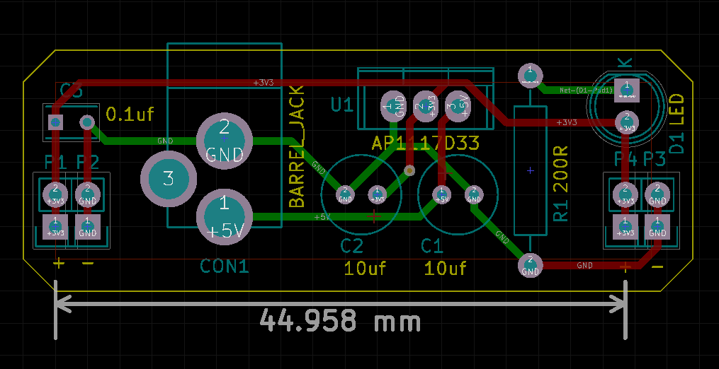
layout

Tips

  • Some operations are easier in default canvas (F9), others in OpenGL (F11)
  • Use the hot keys below!

Kot Keys

  • ? - show hotkeys
  • space - reset local co-ordinates
  • F1 - zoom in
  • F2 - zoom out
  • m - move component (without wires)
  • g - drag component (with wires)
  • del - delete an object
  • F11 - switch to openGL view (necessary for push'n'shove routing)
  • e - routing options (only in openGL)
  • x - start routing
  • pg up - route on top layer
  • pg down - route on bottom layer
  • v - create via
  • f - flip a component between top & bottom layers

Fabrication

Watch the fabrication screencast

Description of layers

  • F.Cu - top copper layer used for electrical connections
  • B.Cu - bottom copper layer (as above)
  • F.SilkS - top silk screen used for component markings and orientation
  • B.SilkS - bottom silk screen (as above)
  • F.Mask - top mask used to cover the electrical connections with a nonconductive coloured layer
  • B.Mask - bottom mask (as above)
  • Edge.Cuts - where the board should be cut out

Each of these layers is exported as a separate file called a gerber.

You also need a drill file that specifies where all the holes are.

Zip all the files together and then upload to OSHPark.com

Parts

100
QtyValueFootprintReferences
5TESTMeasurement_Points:Test_Point!cs1, clk1, gnd1, sdo1, sdo2
31uCapacitors_SMD:C_1206_HandSolderingC1, C2, C5
3CONN_01X02Pin_Headers:Pin_Header_Straight_1x02adc1-in1, adc2-in1, P2
210nCapacitors_SMD:C_1206_HandSolderingC3, C4
2CONN_01X08Pin_Headers:Pin_Header_Straight_1x08ard0, gpio1
2CONN_02X06Pin_Headers:Pin_Header_Straight_2x06pmod1, pmod2
2ads7883TO_SOT_Packages_SMD:SOT-23-6adc1, adc2
1100RResistors_SMD:R_1206_HandSolderingR1
11nfCapacitors_SMD:C_1206_HandSolderingC6
122uCapacitors_SMD:c_elec_6.3x7.7c7
1CONN_01X03Pin_Headers:Pin_Header_Straight_1x03P1
1CONN_02X04Pin_Headers:Pin_Header_Straight_2x04P9
1CONN_02X23Pin_Headers:Pin_Header_Straight_2x23P8
1LEDLEDs:LED-1206D1
1RResistors_SMD:R_1206_HandSolderingR2
1ref5050Housings_SOIC:SOIC-8_3.9x4.9mm_Pitch1.27mmU1

The 28 most common of 100 parts.

More from mattvenn/kicad

12
  • 2 layers100 × 40 mmModbox brain, the printed circuit board in 3D

    Modbox brain

    mattvenn/kicad

    The documentation for this workshop mostly consists of youtube screencasts. The screencasts are deliberately fast, if you need them slower then click the video's settings button and choose a slower speed.

    77 parts14
  • 2 layers100 × 40 mmAttiny88, the printed circuit board in 3D

    Attiny88

    mattvenn/kicad

    The documentation for this workshop mostly consists of youtube screencasts. The screencasts are deliberately fast, if you need them slower then click the video's settings button and choose a slower speed.

    44 parts14
  • 2 layers39 × 39.5 mmDvipmod, the printed circuit board in 3D

    Dvipmod

    mattvenn/kicad

    The documentation for this workshop mostly consists of youtube screencasts. The screencasts are deliberately fast, if you need them slower then click the video's settings button and choose a slower speed.

    42 parts14
  • 2 layers100 × 40 mmModbox lcd, the printed circuit board in 3D

    Modbox lcd

    mattvenn/kicad

    The documentation for this workshop mostly consists of youtube screencasts. The screencasts are deliberately fast, if you need them slower then click the video's settings button and choose a slower speed.

    38 parts14
  • 2 layers90 × 70 mmOobb namebadge, the printed circuit board in 3D

    Oobb namebadge

    mattvenn/kicad

    The documentation for this workshop mostly consists of youtube screencasts. The screencasts are deliberately fast, if you need them slower then click the video's settings button and choose a slower speed.

    28 parts14
  • 2 layersEsp8266 temp, the printed circuit board in 3D

    Esp8266 temp

    mattvenn/kicad

    The documentation for this workshop mostly consists of youtube screencasts. The screencasts are deliberately fast, if you need them slower then click the video's settings button and choose a slower speed.

    17 parts14
  • 2 layers55.9 × 44.5 mmEsp humidity, the printed circuit board in 3D

    Esp humidity

    mattvenn/kicad

    The documentation for this workshop mostly consists of youtube screencasts. The screencasts are deliberately fast, if you need them slower then click the video's settings button and choose a slower speed.

    16 parts14
  • 2 layers53.3 × 40.6 mmEsp8266 breakout, the printed circuit board in 3D

    Esp8266 breakout

    mattvenn/kicad

    The documentation for this workshop mostly consists of youtube screencasts. The screencasts are deliberately fast, if you need them slower then click the video's settings button and choose a slower speed.

    16 parts14
  • 2 layers43 × 33 mmWiimotefpga, the printed circuit board in 3D

    Wiimotefpga

    mattvenn/kicad

    The documentation for this workshop mostly consists of youtube screencasts. The screencasts are deliberately fast, if you need them slower then click the video's settings button and choose a slower speed.

    15 parts14
  • 2 layers57 × 43 mmEsp8266-12-breakout, the printed circuit board in 3D

    Esp8266-12-breakout

    mattvenn/kicad

    The documentation for this workshop mostly consists of youtube screencasts. The screencasts are deliberately fast, if you need them slower then click the video's settings button and choose a slower speed.

    12 parts14
  • 2 layers52.8 × 19 mmBreadboard psu, the printed circuit board in 3D

    Breadboard psu

    mattvenn/kicad

    The documentation for this workshop mostly consists of youtube screencasts. The screencasts are deliberately fast, if you need them slower then click the video's settings button and choose a slower speed.

    11 parts14
  • 2 layers38 × 40 mmEarth to mars, the printed circuit board in 3D

    Earth to mars

    mattvenn/kicad

    The documentation for this workshop mostly consists of youtube screencasts. The screencasts are deliberately fast, if you need them slower then click the video's settings button and choose a slower speed.

    10 parts14

Similar boards

  • 4 layers162.2 × 100 mmDigital, the printed circuit board in 3D

    Digital

    Dawson-HEP/opentrig

    Open-source acquisition trigger

    438 parts6EPL-2.0
  • 4 layers35 × 42 mmADS7883-pmod, the printed circuit board in 3D

    ADS7883-pmod

    mattvenn/ADS7883-pmod

    pmod breakout for 2 x ADS7883 ADC

    31 parts4
  • 2 layers160 × 100 mmPIAD-18bits, the printed circuit board in 3D

    PIAD-18bits

    lnls-sirius/SPIxCONV

    This project consists of an 18-bit analog input (ADC) and output (DAC) within a range of 20 V (± 10 V) and 32 digital pins that can be either as inputs or outputs.

    178 parts1MIT
  • 2 layers156.2 × 141 mmMCU MotherBoard, the printed circuit board in 3D

    MCU MotherBoard

    bc-kim/PCB_KiCAD

    Tips Footprint of the resisotor and capacitor should be assigned aforetime because assigning those are comfusing when lots of reisistor and capacitors are used. 3. Reference: https://wikidocs.net/103412

    49 parts
  • 2 layers40.6 × 23 mmECG, the printed circuit board in 3D

    ECG

    IIBM/stethoscope

    28 parts
  • 2 layers28 × 100 mmAttenuverter, the printed circuit board in 3D

    Attenuverter

    ojz/prompted-circuit-boards

    Prompt-driven design of Eurorack modules with KiCad 10

    31 parts

Questions

How big is the Bbb adc PCB?

It measures 65 × 78 mm and has 2 copper layers, 1.6 mm thick.

What parts does the Bbb adc use?

100 parts, built around the REF5050ID. The full list of its parts is on this page, with links to each part's symbol and footprint where PCBKit's library has them.

Where can I download the Bbb adc KiCad files?

From the mattvenn/kicad repository on GitHub, at the commit this page was made from: the board is bbb-adc/bbb-adc.kicad_pcb. PCBKit opens the board in the browser, with nothing to install.

Can I use the Bbb adc design in my own project?

Its repository states no licence, so its author keeps all rights: ask mattvenn before reusing the design.