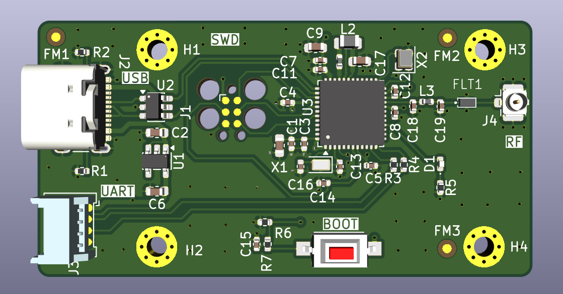
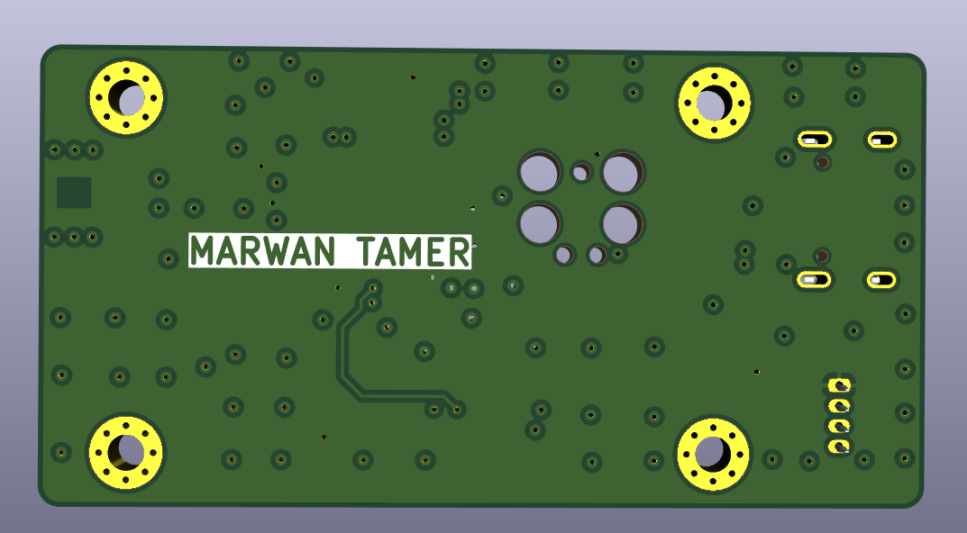
STM32-Bluetooth is an open-source printed circuit board by marwantm, from the marwantm/STM32-Bluetooth repository on GitHub. It is a 4-layer board of 54.2 × 28.1 mm with 48 parts on 55 nets, routed with 268 tracks and 102 vias.
It is built around the STM32WB55CEU6, MIC5365-3.3YD5-TR and USBLC6-2SC6. Its parts include 19 capacitors, 7 resistors, 4 connectors, 3 ICs and 3 inductors. It belongs with the radio and wireless and microcontroller boards boards and the STM32 boards of this library.
A 4-layer STM32WB55-based Bluetooth Low Energy development board, designed in KiCad by following Phil's Lab's professional PCB design tutorial — built to strengthen my understanding of the full schematic-to-manufacturing workflow, not just replicate the steps.
Overview
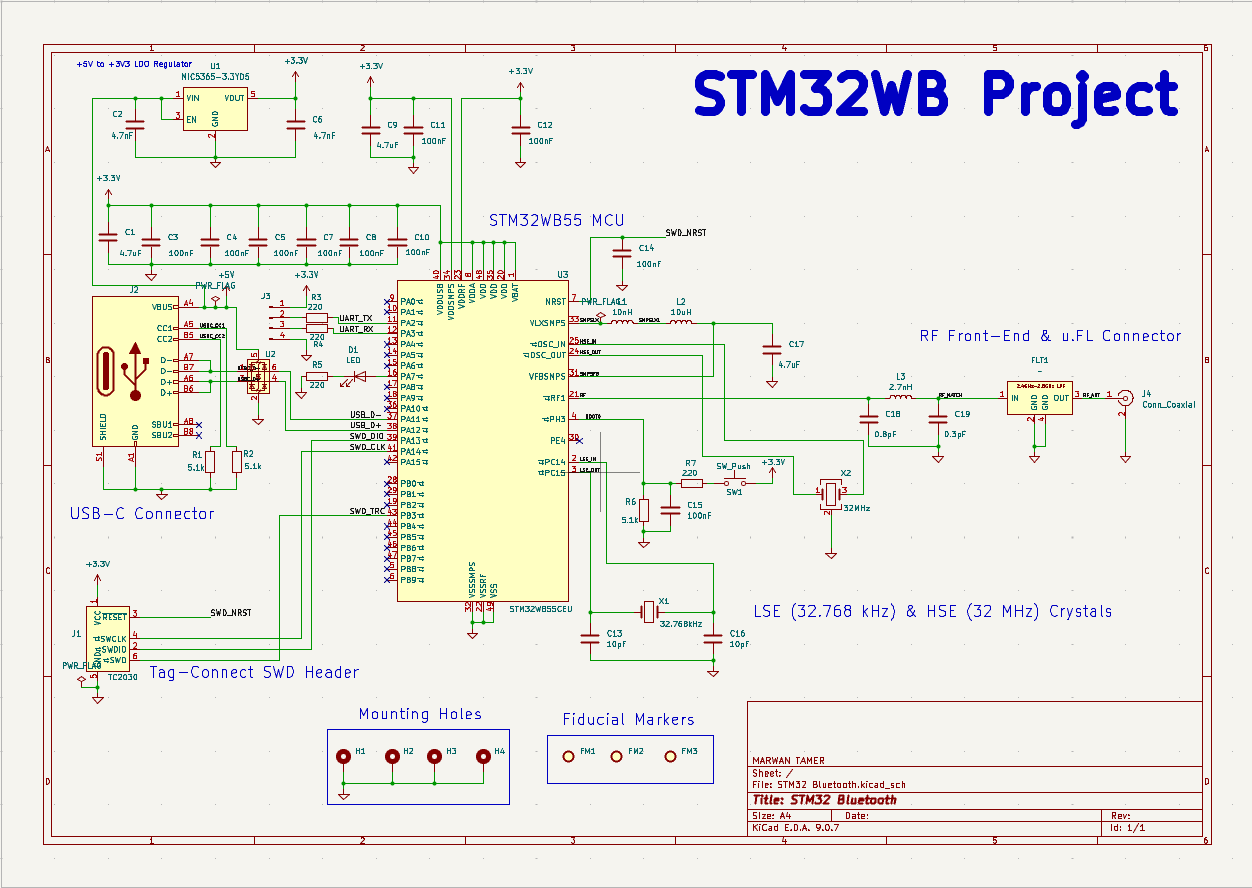
This board is built around the STM32WB55CEU, a dual-core MCU with an integrated BLE radio. It includes USB-C power/data, a UART header, an SWD programming interface, an RF front-end with a u.FL antenna connector, and a boot/reset button — a complete minimal BLE development platform.
MCU
STM32WB55CEU (Cortex-M4 + BLE co-processor)
Connectivity
Bluetooth Low Energy (2.4 GHz), USB-C, UART
PCB
4-layer (Signal / GND / Power / Signal)
Programming
SWD via Tag-Connect TC2030
Power
USB-C (5V → 3.3V via onboard LDO)
Design Tool
KiCad 9
What I Learned
Following Phil's Lab's tutorial, I worked through the reasoning behind each design decision rather than just replicating the steps:
Schematic Design
Structuring the schematic into logical functional blocks (power, MCU, USB, RF front-end, programming header)
Organizing components and net labels for readability rather than just electrical correctness
Keeping the design navigable for anyone reviewing it later, not just the person who built it
PCB Layout
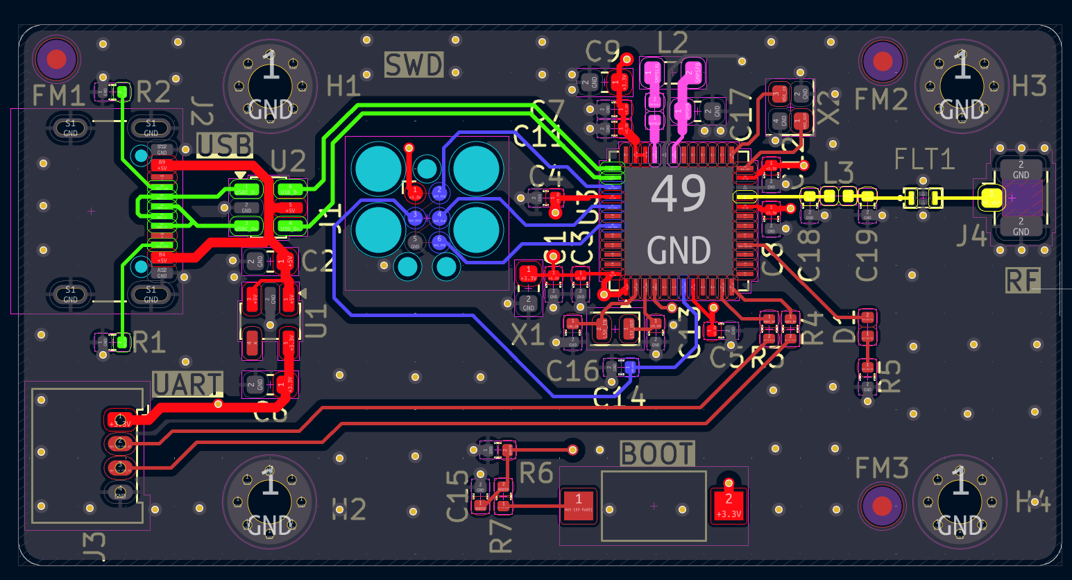
Component placement strategy before routing — placing by function and signal criticality, not just by convenience
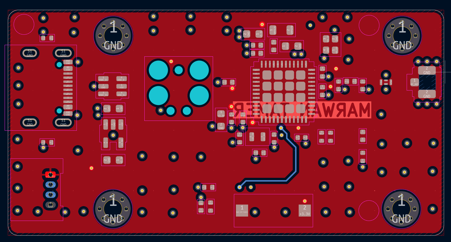
Working with a 4-layer stack-up (Signal / GND plane / Power plane / Signal)
Correct use of vias, mounting holes (including plated vs. non-plated, with-via vs. without), and fiducials for pick-and-place accuracy
Designing dedicated ground and power planes rather than routing power as traces
Routing strategy for RF, high-speed, and power nets, and resolving DRC/ERC violations until the board passed clean
Built by following Phil's Lab's STM32WB Bluetooth tutorial. This project is a learning exercise, not an original design — full credit for the schematic architecture and design decisions goes to Phil's Lab's tutorial series.
Author
Marwan Tamer
Electrical Power Engineering student, building toward Embedded Systems Engineering
LinkedIn
Designed a compact embedded system integrating USB-C, power management, and RF design into a single 4-layer PCB. Focused on clean layout, strong signal integrity, and practical debugging structure.
Custom STM32WB55 development board integrating 2.4GHz BLE 5.x, LPUART, I2C, and UART via RS232/DB9 for PC and industrial machine interfacing. Designed to bridge modern wireless IoT with legacy wired systems.
It measures 54.2 × 28.1 mm and has 4 copper layers, 1.58 mm thick.
What parts does the STM32-Bluetooth use?
48 parts, built around the STM32WB55CEU6, MIC5365-3.3YD5-TR and USBLC6-2SC6. The full list of its parts is on this page, with links to each part's symbol and footprint where PCBKit's library has them.
Where can I download the STM32-Bluetooth KiCad files?
From the marwantm/STM32-Bluetooth repository on GitHub, at the commit this page was made from: the board is Source_Files/STM32 Bluetooth.kicad_pcb and its schematic Source_Files/STM32 Bluetooth.kicad_sch. PCBKit opens the board in the browser, with nothing to install.
Can I use the STM32-Bluetooth design in my own project?
Its repository states no licence, so its author keeps all rights: ask marwantm before reusing the design.