6 layers87.8 × 48.3 mm
Bath clamp
lucask07/covg_clamp
kicad schematic and layout for COVG bath and guard clamps
183 partsGPL-3.0

 lucask07/open_covg_daq_pcb9
DAQ (ADCs and DACs) PCB for the digital ion channel amplifier project.
Covg daq v2 is an open-source printed circuit board by lucask07, from the lucask07/open_covg_daq_pcb repository on GitHub, published under the GPL-3.0 licence. It is a 6-layer board of 157.8 × 95.2 mm with 600 parts on 555 nets, routed with 13,162 tracks and 1,445 vias.
It is built around the OPA1662AID, AD7961BCPZ-RL7 and DAC80508ZRTER, with the TCA9555PW, ADS8686SIPZAR and TXS0108EPW among its other parts. Its parts include 286 resistors, 211 capacitors, 64 ICs, 14 connectors and 3 inductors. It belongs with the audio and music boards of this library.


This repository houses the KiCad schematic, layout, and BOM for a general-purpose data acquisition board (DAQ) that enables real-time feedback with latencies of < 2 us by direct interfaces of ADCs and DACs to the XEM7310 OpalKelly FPGA module. This DAQ board is designed for a digital feedback implementation of a clamp amplifier for the cut-open vaseline gap (COVG) electrophysiology method and may also find a use for other scientific studies requiring low latency control.
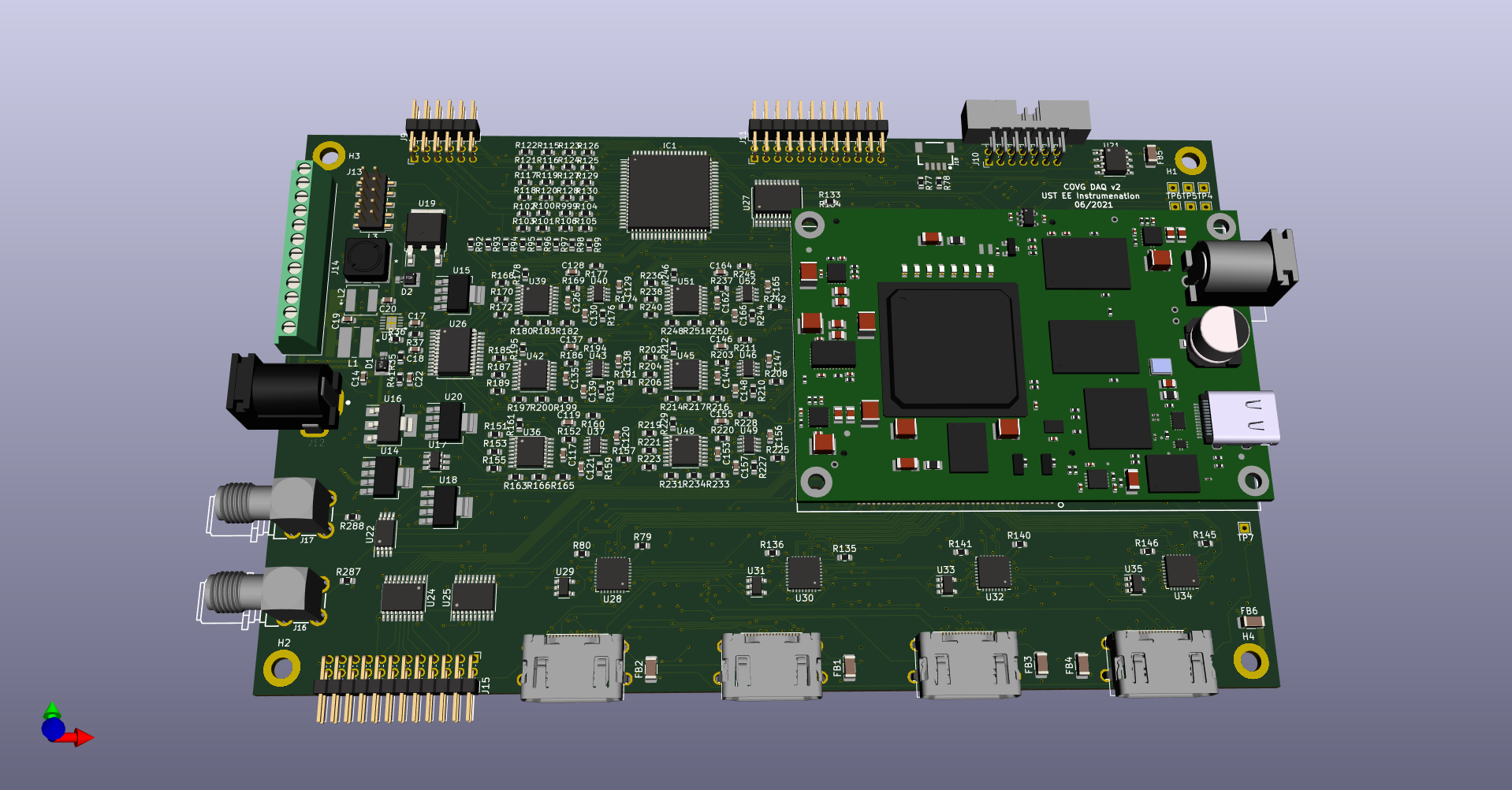
The schematic is here and a 3d rendering of the board is shown below:
Contact: Lucas Koerner at the University of St. Thomas, School of Engineering using the email: koerner dot lucas at stthomas.edu.
At connector J15:
At connector J10:
At SMA connectors J16 and J17:
At QWIIC connector, J18:
An input voltage of 6 to 7V is supplied at barrel connector J12 (PJ-002BH) with a maximum rating of 5 A.
The power system is as follows:
All power nets are connected to a screw terminal block connector to allow for monitoring or override of the on-board regulated voltages.
The XEM7310 OpalKelly FPGA module has a Artix7 FPGA (XC7A5T-1) with a USB 3.0 interface to a host computer (transfer rates up to 30 MiB/s). The module has 1-GiByte of DDR3 to enable burst data captures or burst data transfers.
The DAQ board has four connections to support analog daughtercards. The daughtercard connections are standardized and use an HDMI connector. For the COVG electrophysiology amplifier, these channels are the bath clamp, guard clamp, V1/I top clamp, and (optionally) the V2 monitor. Future experiments could use one or up to all of these daughtercard connections.
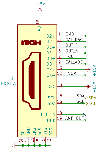
The generic HDMI-A cable pinout is defined as follows with 15 (non-shield) pins used:
| Pin | HDMI name | Generic Daughtercard | Notes |
|---|---|---|---|
| 1 | Data2+ | fastDAC1 | ~ 1 us settling time. Programmable full-scale range. |
| 2 | Data2 shield | gnd | |
| 3 | Data2- | Analog/GPIO1 | DAC8050, 16 bit, 5us settle, 5 V supply |
| 4 | Data1+ | fastADC+ | Analog output to AD7960/AD7961. Differential low-pass filter on DAQ board. Common mode voltage must match 2.5 V. |
| 5 | Data1 shield | gnd | |
| 6 | Data1- | fastADC- | Analog output to AD7960/AD7961. Differential low-pass filter on DAQ board. Common mode voltage must match 2.5 V. |
| 7 | Data0+ | fastDAC2 | ~1 us settling time. Programmable full-scale range. |
| 8 | Data0 shield | gnd | |
| 9 | Data0- | Analog/GPIO2 | Analog output to ADS8686 1 MSPS. Chip inputs includes a programmable PGA for full-scale range up to +/-10V |
| 10 | Clock+ | 15V | linear regulator, 75 mA max per channel |
| 11 | Clock shield | gnd | |
| 12 | Clock- | VCM | reference voltage from the AD796x buffered on the DAQ board, nominal 2.5 V |
| 13 | CEC | -15V | linear regulator, (estimate is 75 mA max per channel with all 4 channels connected) |
| 14 | Reserved | selectable auxillary | Resistor jumper sets analog in, analog out, or digital I/O (@ 3.3 V levels). Default stuffing option is to connect to the general purpose ADC (ADS8686). |
| 15 | SCL | SCL | I2C clock. Pull-up resistor on DAQ board, 3.3 V levels. |
| 16 | SDA | SDA | I2C data. Pull-up resistor on DAQ board, 3.3 V levels. |
| 17 | Gnd | Gnd | |
| 18 | 5V | 5V | Power from linear regulator (target 200 mA max per channel with all 4 channels connected) |
| 19 | HPD | Analog/GPIO3 | Analog output to ADS8686 1 MSPS. Chip inputs includes a programmable PGA for full-scale range up to +/-10V |
The pin names shown in the image below are an example daughtercard interface (COVG bath-clamp).
Because of the LVDS connections to the AD7961 FPGA bank 34 needs to be at 2.5 V. To do so remove ferrite bead (FB8) from the OpalKelly module. See the section "Setting the Expansion Connector I/O Voltages" here.
Symbols and footprints custom to this design (and the COVG project in general) are housed in the covg-kicad-lib repository. This library should be a project specific library in your KiCAD Symbol Library Management and Footrpint Library Management.
When at all possible, footprints are used from the KiCAD libraries.
Impedance control of the LVDS lines to the AD796x was done using the 6-layer stackup from PCBWAY with board thickness of 1.6 mm and copper (outer/inner) thickness of 1oz/1oz. The design has the impedance-controlled LVDS signals routed on the top or bottom layer (and therefore a microstrip referenced to layer 2 or layer 15). The differential pairs are skew matched on both the DAQ board and the FPGA modules. The (inter pair) signals for each AD796x have effectively a half clock cycle of slack for skew so are reasonably but not precisely length matched. The DCO signal (AD796x clock out) is routed to a clock capable pin on the XEM7310.
The AD796x impedance controlled differential pairs were routed using the KiCAD differential pair tool and the power planes were drawn in KiCAD to match the location of the various power domains. Parts were placed manually and the 'Replicate layout' KiCAD plug-in was used to duplicate the placement of identical blocks. Then the board was exported to use the tool freerouting to route most of the board. After freerouting it was found to be critical to confirm that inner layer routing did not destroy the integrity of the power planes.
pinout of the Artix7
The KiCAD schematic uses a field Manf# to specify the precise manufacturer's part number for component sourcing. This also allows the (great) KiCAD External Plugin KiCost to be used to check board component cost and availability. One complication is that the OpalKelly XEM7310 exports as one BOM line item. Ultimately, though, the board must be populated with two Samtec BTE-040-02-F-D-A high-density connectors at silk-screen labels MC1 and MC2. See the part position file:
MC1 Connector_SMD BTE-040-02-F-D-A 108.6849 33.1811 180.0000 top
MC2 Connector_SMD BTE-040-02-F-D-A 108.6849 73.1911 180.0000 top
The bill of materials files are here.
Note that the "chip shortage of 2020/2021" has made component sourcing complicated and we hope this bottle-neck eases in the near future.
The prototype boards were assembled by PCBWAY. The information provided to the assembly house is in the assembly folder.
Please see the issues section of the GitHub repository. The most significant considerations are:
Unconnected level translator pins unused inputs The level translator used can leave unused pins disconnected.
Barrel jack: The Opal Kelly FPGA barrel connector is 2.1 mm ID / 5.5 mm OD while the DAQ board power jack 2.5 mm ID / 5.5 mm OD are different sizes.
Why do the barrel jacks have 3-pins and what to do with the 3rd pin? 3-pin DC jack
HDMI cable casing is 20 mm so at least 25 mm pitch is needed between connectors.
Research reported in this publication was supported by the National Institute Of Neurological Disorders And Stroke of the National Institutes of Health under Award Number R15NS116907. The content is solely the responsibility of the authors and does not necessarily represent the official views of the National Institutes of Health.
Copyright 2021 Lucas J. Koerner.
See the Git repo for License details.
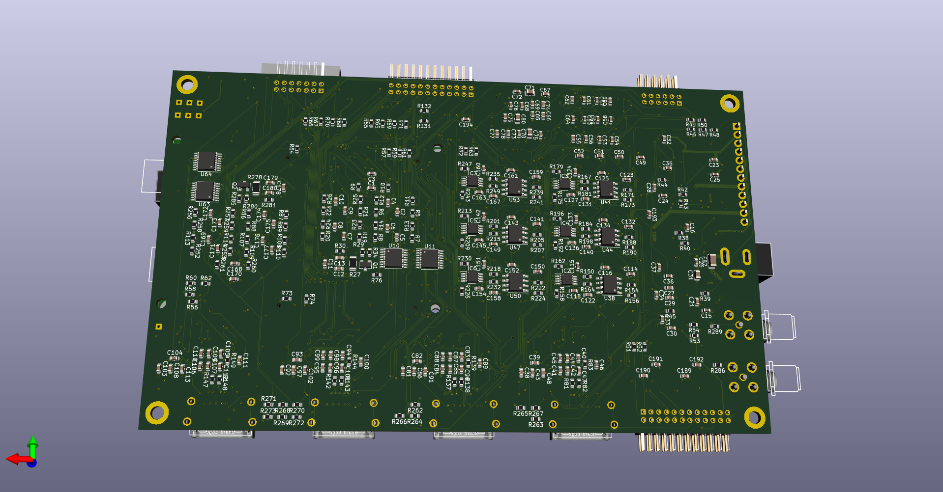
Boards were fabricated and assembled by PCBWAY (https://www.pcbway.com/).

| Qty | Value | Footprint | References |
|---|---|---|---|
| 117 | 0.1u | Capacitor_SMD:C_0603_1608Metric | C1, C10, C100, C102, C103, C104, C105, C107, C108, C109, C110, C111, C113, C115, C116, C118 +101 |
| 51 | 33 | Resistor_SMD:R_0603_1608Metric | R10, R132, R133, R134, R137, R138, R139, R142, R143, R144, R147, R148, R149, R152, R157, R158 +35 |
| 40 | 1k | Resistor_SMD:R_0603_1608Metric | R100, R101, R102, R103, R104, R105, R106, R115, R116, R117, R118, R119, R120, R121, R122, R123 +24 |
| 29 | DNI | Capacitor_SMD:C_0603_1608Metric | C20, C49, C50, C51, C114, C117, C123, C126, C132, C135, C141, C144, C150, C153, C159, C162 +13 |
| 24 | 10k | Resistor_SMD:R_0603_1608Metric | R1, R2, R15, R16, R17, R18, R111, R112, R162, R179, R196, R213, R230, R247, R254, R255 +8 |
| 23 | 0 | Resistor_SMD:R_0603_1608Metric | R29, R30, R46, R160, R177, R194, R211, R228, R245, R260, R266, R267, R268, R269, R280, R281 +7 |
| 18 | 15k | Resistor_SMD:R_0603_1608Metric | R11, R12, R13, R14, R23, R24, R25, R26, R36, R43, R109, R110, R252, R253, R258, R259 +2 |
| 18 | 5p | Capacitor_SMD:C_0603_1608Metric | C11, C178, C195, C196, C197, C198, C199, C200, C201, C202, C203, C204, C205, C206, C207, C208 +2 |
| 16 | 30.1k | Resistor_SMD:R_0603_1608Metric | R5, R6, R7, R8, R19, R20, R21, R22, R86, R87, R107, R108, R113, R114, R256, R257 |
| 15 | DNI | Resistor_SMD:R_0603_1608Metric | R35, R42, R64, R73, R74, R262, R263, R264, R265, R270, R271, R272, R273, R286, R289 |
| 14 | 3.3k | Resistor_SMD:R_0603_1608Metric | R51, R52, R54, R55, R57, R59, R61, R63, R65, R69, R71, R72, R77, R78 |
| 14 | OPA2156xD | Package_SO:SOIC-8_3.9x4.9mm_P1.27mm | U1, U2, U3, U4, U6, U7, U8, U9, U38, U41, U44, U47, U50, U53 |
| 12 | 20k | Resistor_SMD:R_0603_1608Metric | R161, R163, R178, R180, R195, R197, R212, R214, R229, R231, R246, R248 |
| 9 | 100k | Resistor_SMD:R_0603_1608Metric | R38, R39, R40, R44, R45, R58, R60, R62, R131 |
| 9 | 10u | Capacitor_SMD:C_0603_1608Metric | C41, C65, C66, C67, C68, C77, C84, C95, C106 |
| 8 | 100 | Resistor_SMD:R_0603_1608Metric | R79, R80, R135, R136, R140, R141, R145, R146 |
| 8 | 1u | Capacitor_SMD:C_0603_1608Metric | C15, C21, C24, C28, C30, C33, C36, C37 |
| 8 | 470k | Resistor_SMD:R_1206_3216Metric | R27, R28, R31, R32, R278, R279, R282, R283 |
| 7 | TestPoint | TestPoint:TestPoint_THTPad_1.5x1.5mm_Drill0.7mm | TP1, TP2, TP3, TP4, TP5, TP6, TP7 |
| 6 | 121k | Resistor_SMD:R_0603_1608Metric | R153, R170, R187, R204, R221, R238 |
| 6 | 2.4n | Capacitor_SMD:C_0603_1608Metric | C122, C131, C140, C149, C158, C167 |
| 6 | 243k | Resistor_SMD:R_0603_1608Metric | R151, R168, R185, R202, R219, R236 |
| 6 | 2k | Resistor_SMD:R_0603_1608Metric | R164, R181, R198, R215, R232, R249 |
| 6 | 2p | Capacitor_SMD:C_0603_1608Metric | C119, C128, C137, C146, C155, C164 |
| 6 | 3.24k | Resistor_SMD:R_0603_1608Metric | R156, R173, R190, R207, R224, R241 |
| 6 | 37.4k | Resistor_SMD:R_0603_1608Metric | R154, R171, R188, R205, R222, R239 |
| 6 | 49.9k | Resistor_SMD:R_0603_1608Metric | R150, R167, R184, R201, R218, R235 |
| 6 | 8.25k | Resistor_SMD:R_0603_1608Metric | R155, R172, R189, R206, R223, R240 |
| 6 | AD5453 | Package_TO_SOT_SMD:TSOT-23-8 | U37, U40, U43, U46, U49, U52 |
| 6 | Ferrite_Bead | Capacitor_SMD:C_1206_3216Metric | FB1, FB2, FB3, FB4, FB5, FB6 |
| 6 | OPA1662 | Package_SO:VSSOP-8_3.0x3.0mm_P0.65mm | IC2, IC3, IC4, IC5, IC6, IC7 |
| 6 | TMUX6111PWR | Package_SO:TSSOP-16_4.4x5mm_P0.65mm | U36, U39, U42, U45, U48, U51 |
| 5 | 10u | Capacitor_SMD:C_0805_2012Metric | C31, C70, C71, C80, C211 |
| 4 | 100p | Capacitor_SMD:C_0603_1608Metric | C47, C90, C101, C112 |
| 4 | AD7961BCPZ-RL7 | Package_DFN_QFN:QFN-32-1EP_5x5mm_P0.5mm_EP3.1x3.1mm | U28, U30, U32, U34 |
| 4 | DNI | MountingHole:MountingHole_3.2mm_M3_DIN965_Pad | H1, H2, H3, H4 |
| 4 | HDMI_A | covg-kicad:CONN_10029449-111RLF_HDMI_A | J1, J2, J7, J8 |
| 4 | OPA325 | Package_TO_SOT_SMD:SOT-23-5 | U29, U31, U33, U35 |
| 4 | TMUX6136PWR | Package_SO:TSSOP-16_4.4x5mm_P0.65mm | U10, U11, U63, U64 |
| 3 | 4.7u | Capacitor_SMD:C_0603_1608Metric | C14, C19, C25 |
| 2 | 0.33u | Capacitor_SMD:C_0603_1608Metric | C18, C22 |
| 2 | 1u | Capacitor_SMD:C_1206_3216Metric | C32, C35 |
| 2 | 33p | Capacitor_SMD:C_0603_1608Metric | C16, C23 |
| 2 | 4.7k | Resistor_SMD:R_0603_1608Metric | R37, R41 |
| 2 | 470k | Resistor_SMD:R_0603_1608Metric | R33, R284 |
| 2 | 49.9 | Resistor_SMD:R_0603_1608Metric | R287, R288 |
| 2 | BC856 | Package_TO_SOT_SMD:SOT-23 | Q1, Q2 |
| 2 | Conn_02x12_Odd_Even | Connector_PinHeader_2.00mm:PinHeader_2x12_P2.00mm_Horizontal | J11, J15 |
| 2 | Conn_Coaxial | covg-kicad:BU-SMA-G | J16, J17 |
| 2 | DAC80508ZRTER | Package_DFN_QFN:WQFN-16-1EP_3x3mm_P0.5mm_EP1.6x1.6mm | U5, U58 |
| 2 | DNI | Diode_SMD:D_Powermite_AK | D1, D2 |
| 2 | OPA991S | Package_TO_SOT_SMD:SOT-23-6 | U12, U65 |
| 2 | TCA9555 | Package_SO:SSOP-24_5.3x8.2mm_P0.65mm | U26, U27 |
| 2 | TXS0108EPW | Package_SO:TSSOP-20_4.4x6.5mm_P0.65mm | U24, U25 |
| 1 | 24AA025UID | Package_SO:SOIC-8_3.9x4.9mm_P1.27mm | U21 |
| 1 | ADS8686SIPZAR | Package_QFP:LQFP-80_14x14mm_P0.65mm | IC1 |
| 1 | Conn_01x06 | covg-kicad:Molex_6Pin_CONN | J3 |
| 1 | Conn_02x05_Odd_Even | Connector_PinHeader_2.00mm:PinHeader_2x05_P2.00mm_Vertical_SMD | J13 |
| 1 | Conn_02x06_Odd_Even | Connector_PinHeader_2.00mm:PinHeader_2x06_P2.00mm_Horizontal | J9 |
| 1 | Conn_02x07_Odd_Even | Connector_PinHeader_2.00mm:PinHeader_2x07_P2.00mm_Horizontal | J10 |
| 1 | DNI | covg-kicad:SRR4018-4R7Y | L1 |
| 1 | DNI | covg-kicad:SRR6028-150Y | L3 |
| 1 | DNI | covg-kicad:NRS5020T100MMGJ | L2 |
| 1 | DNI | covg-kicad:DFN-10-1EP_3x3mm_P0.5mm_EP1.65x2.38mm | U13 |
| 1 | LM2937xMP | Package_TO_SOT_SMD:SOT-223-3_TabPin2 | U16 |
| 1 | LP38692MP-5.0 | Package_TO_SOT_SMD:SOT-223-5 | U14 |
| 1 | LP38693MP-1.8 | Package_TO_SOT_SMD:SOT-223-5 | U18 |
| 1 | LP38693MP-2.5 | Package_TO_SOT_SMD:SOT-223-5 | U20 |
| 1 | LP38693MP-3.3 | Package_TO_SOT_SMD:SOT-223-5 | U15 |
| 1 | MAX6070BAUT21+T | Package_TO_SOT_SMD:SOT-23-6_Handsoldering | U17 |
| 1 | MC7915BD2TR4G | Package_TO_SOT_SMD:TO-263-3_TabPin2 | U19 |
| 1 | NLSX3018DTR2G | Package_SO:TSSOP-20_4.4x6.5mm_P0.65mm | U23 |
| 1 | OPALKELLY_XEM7310 | covg-kicad:OPALKELLY_XEM7310 | OK1 |
| 1 | PCA9306 | Package_SO:TSSOP-8_4.4x3mm_P0.65mm | U22 |
| 1 | QWIIC_CONNECTOR-1MM | Connectors:1X04_1MM_RA | J18 |
| 1 | Screw_Terminal_01x12 | TerminalBlock_Phoenix:TerminalBlock_Phoenix_MPT-0,5-12-2.54_1x12_P2.54mm_Horizontal | J14 |
lucask07/covg_clamp
kicad schematic and layout for COVG bath and guard clamps

fablabbcn/smartcitizen-kit-gases-pro-board
Smart Citizen Kit Gases Pro Board

fu5ha/rgba
Reasonably Good Bluetooth Audio - A tiny, inline Bluetooth audio receiver for IEMs.


rf-designers/transceiver
Repository containing the design for the YO6SSW SDR transceiver, version 2


It measures 157.8 × 95.2 mm and has 6 copper layers, 1.6 mm thick.
600 parts, built around the OPA1662AID, AD7961BCPZ-RL7, DAC80508ZRTER and TCA9555PW. The full list of its parts is on this page, with links to each part's symbol and footprint where PCBKit's library has them.
From the lucask07/open_covg_daq_pcb repository on GitHub, at the commit this page was made from: the board is covg_daq_v2.kicad_pcb and its schematic adc.kicad_sch. PCBKit opens the board in the browser, with nothing to install.
Its repository publishes it under the GPL-3.0 licence: you may reuse it on that licence's terms (keep the author's notice, and for a copyleft licence share your changes alike).