6 layers157.8 × 95.2 mm
Covg daq v2
lucask07/open_covg_daq_pcb
DAQ (ADCs and DACs) PCB for the digital ion channel amplifier project.
600 parts9GPL-3.0

 lucask07/covg_clamp
kicad schematic and layout for COVG bath and guard clamps
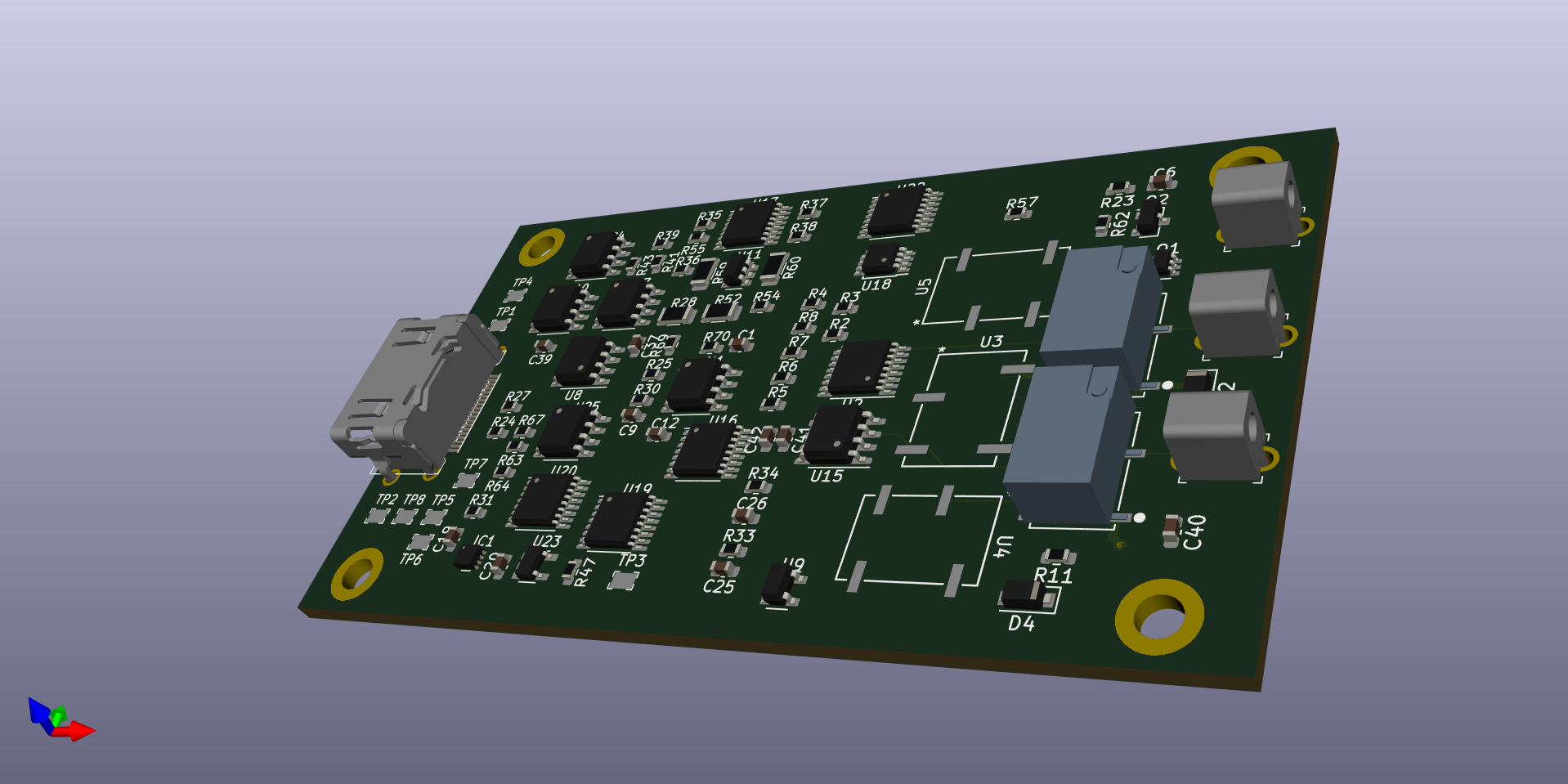
Bath clamp is an open-source printed circuit board by lucask07, from the lucask07/covg_clamp repository on GitHub, published under the GPL-3.0 licence. It is a 6-layer board of 87.8 × 48.3 mm with 183 parts on 164 nets, routed with 2,107 tracks and 294 vias.
It is built around the OPA828ID, AD8421ARZ and G6L-1F-TR-DC5, with the 24AA025UID-I/P, ADG1208YRZ and RCT-0C among its other parts. Its parts include 74 resistors, 49 capacitors, 26 ICs, 5 diodes and 5 connectors.


Schematic and layout for the COVG bath and guard clamps. This board sits near electrodes and includes a force output and a high-impedance feedback input to create a closed-loop clamp. Intention is to use the same design for the bath and guard clamps of a COVG amplifiers. The board supports digital programming of the current measurement gain and the feedback loop stability. Switching on the board allows for connect and disconnect of electrodes and injection (or measurements) of calibration signals onto an electrode.
If this work contributes to your research please cite:
I. Delgadillo Bonequi, A. Stroschein, and L. J. Koerner, “A field-programmable gate array (FPGA)-based data acquisition system for closed-loop experiments,” Review of Scientific Instruments, vol. 93, no. 11, p. 114712, Nov. 2022, doi: 10.1063/5.0121898.
The digital COVG project uses the concept of one main data acquition board connected to an FPGA. The main data acquisition board has multiple channels that extend to daughtercards. The connection to each daughtercard allows for low-latency control by connections to high-speed ADCs and DACs on the daq board. For COVG the daughtercards are the bath clamp; the guard clamp; the voltage clamp and I force; and the V1/V2. The connectivity to the daughtercard is generalized and will be the same for each.
An HDMI-A cable is used for input and output signals that connects the bath clamp daughtercard to the DAQ board. The HDMI cable carries:

| Pin | HDMI name | Generic Daughtercard | Bath clamp | Notes |
|---|---|---|---|---|
| 1 | Data2+ | fastDAC1 | CMD | ~1 us settling time |
| 2 | Data2 shield | Gnd | Gnd | |
| 3 | Data2- | Analog/GPIO1 | CAL_DAC | Analog input signal from DAC8050, 16 bit, 5us settle, 5 V supply |
| 4 | Data1+ | fastADC+ | IM_P | to AD7960/AD7961. Differential low-pass filter on DAQ board |
| 5 | Data1 shield | Gnd | Gnd | |
| 6 | Data1- | fastADC- | IM_N | to AD7960/AD7961. Differential low-pass filter on DAQ board |
| 7 | Data0+ | fastDAC2 | CC | ~1 us settling time |
| 8 | Data0 shield | Gnd | Gnd | |
| 9 | Data0- | Analog/GPIO2 | CAL_ADC | to ADS8686 1 MSPS, programmable PGA for range up to +/-10V |
| 10 | Clock+ | 15V | 15V | From a linear regulator on the DAQ board, 75 mA max per channel |
| 11 | Clock shield | Gnd | Gnd | |
| 12 | Clock- | VCM | VCM | buffered on DAQ board, nominal 2.5 V |
| 13 | CEC | -15V | -15V | From a linear regulator on the DAQ board, 75 mA max per channel |
| 14 | Reserved | open | open | Resistor jumper on DAQ board sets as analog in, analog out, or digital I/O (@ 3.3 V levels). Default stuffing option is to connect to the general purpose ADC (ADS8686). |
| 15 | SCL | SCL | SCL | I2C clock. Pull-up on main DAQ board, 3.3 V levels |
| 16 | SDA | SDA | SDA | I2C data. Pull-up on main DAQ board, 3.3 V levels |
| 17 | Gnd | Gnd | Gnd | |
| 18 | 5V | 5V | 5V | Power input from linear regulator, 200 mA max per channel (target) |
| 19 | HPD | Analog/GPIO3 | AMP_OUT | output to ADS8686 1 MSPS, programmable PGA |
The electrode connections are tip jack miniature PCB mount connectors for 0.08" diameter pin connections.
Electrode diagnositcs / calibration / system ID
Five relays are used to:
Calibration When "calibrating" the electrode that is driven by a DAC signal or output along the ADC signal CAL_ADC is programmable. This output multiplexing is set by DAC_SEL[1..4] and ADC_SEL[1..4]. Via DAC_SEL[1..4] an electrode can be connected to CAL_DAC or GND. The ADC_SEL[1..4] controls the signal that is connected to CAL_ADC pin the options are (CAL_SIG1, CAL_SIG2, INAMP_OUT, CC).
Clamping
Voltage clamp: U1 drives the command voltage (CMD) to electrode P2. Nominal voltage clamp mode will have all 5 relays in nominal position (with 0 coil current). When in voltage clamp mode the current to P2 (as measured by the voltage across nets RF_1 and P2) is output by the different ADC driver for 5 MSPS digitization. The settings for U22 (TMUX6136) are S1 = 1 for the inamp output to be buffered out to the 5 MSPS ADC; and S2 = 1 so that the instrumentation amplifier amplifies the voltage difference: (P2 - RF_1). The voltage feedback in voltage clamp mode can be enabled/disabled by the I/O expander siganl FDBK (FDBK=0 is disabled).
Current clamp: The board has a Howland current source that can be used to set the current to P2 based upon the CMD signal (requires A2=A1=A0=0). The output current can range from +/-0.26 nA (with a 1.22 mV CMD) to +/-2.1 uA (with a 10 V CMD signal). To enable the current clamp either float or drive high the signal EN_IPUMP. To shutoff the amplifier set EN_IPUMP to a logical 0. When in current clamp mode the intent is that the 5 MSPS ADC measurement is of P1 (i.e. set current and measure voltage). This is accomplished by these settings for U22 (TMUX6136): S1 = 0 so that the P2 buffer output voltage is sent to the 5 MSPS ADC; and S2 = 0 so that the instrumentation amplifier amplifies P2 - 0 (RF_1 voltage will not make sense in this mode). In this mode the instrumentation amplifier output can buffer out the CAL_OUT line to a 1 MSPS ADC channel.
The P2 signal is amplified and buffered before being fedback to the main clamp amplifier (U15 within feedback_buffer). The stability of this loop varies depending upon the load presented by the cell under test, electrode electrical characteristics, and parasitic capacitive coupling between electrodes. The stability of this feedback loop can be adjusted by modification of the feedback buffer gain and by changing the capacitance of a lead compensator at the summing junction of the main amplifier (inverting terminal).
Feedback buffer gain
The feedback buffer is a non-inverting structure with an adjustable gain set by I/O expander bits RF[1..4]. The feedback resistor values are 3.01k, 12.1k, 30.1k, and 60.4k. The resistor from the inverting terminal to "ground" is 3.01k creating gains of
Feedback buffer offset
The feedback buffer has offset adjustment. This is generated by a 10-bit I2C interface DAC, IC1 (DAC53401), followed by a unipolar to bipolar amplifier (U23). The output of the bipolar converter ranges between +/-1 V (resolution of 1.9 mV / bit). OUT = VDAC*1.666-1.
(simulation: non_inverting_rpot_bw.asc)
Compensation adjustment
Adjustments of the closed-loop stability are achieved using four approaches.
The current measurement gain (historically reported in units of mV/nA) is determined by three separate "stages".
Resolving inline resistor: is set by component U2 which is an analog switch (ADG1208) that determines the resistance across which the clamp current is measured.
| Ref. Des. | Value | mV/nA | A2,A1,A0 | Closed Switch |
|---|---|---|---|---|
| none -> Iclamp | n/a | n/a | 0,0,0 | Sw1 |
| R2 | 10 kOhm | 0.01 | 0,0,1 | Sw2 |
| R3 | 33.2 kOhm | 0.033 | 0,1,0 | Sw3 |
| R4 | 100k Ohm | 0.1 | 0,1,1 | Sw4 |
| R5 | 332 kOhm | 0.332 | 1,0,0 | Sw4 |
| R6 | 1 MOhm | 1 | 1,0,1 | Sw5 |
| R7 | 3.32 MOhm | 3.32 | 1,1,0 | Sw6 |
| R8 | 10 MOhm | 10 | 1,1,1 | Sw7 |
Instrumentation Amplifier gain
There is a second stage that allows for additional gain on the analog output signal before ADC conversion. The gain of the instrumentation amplifier (AD8421) within the adc_driver block gain is adjusted with bits G[1..3]. The gain options as controled by U17 (DG412 switch) are:
For the instrumentation amplifier Gain = 1 + 9.9 kOhm/RG
Output ADC driver gain
The ADC output driver implements a gain of around 1/3 (0.308 = 499 Ohms/(1500 + 120) Ohms) to scale the maximum output of the instrumenation amplifer (+/-13.5 V) to the range of the AD796x ADC (+/-4.096 V).
Total gain
(without the G = 50 option of the instrumentation amplifier) the available gain ranges are:
Since the ADC covers a range of +/-4.096 V at 16-bit resolution for step-sizes of:
The amplifier noise simulates to be (very roughly) 1 nA RMS, such that ADC quantization noise will not limit amplifier performance when high-gain settings are used.
| Component | Description | I2C address | I2C mode |
|---|---|---|---|
| U12 | I/O expander 0: TCA9555 | 0x26 = 'b010_0110 | Standard, Fast |
| U13 | I/O expander 1: TCA9555 | 0x20 = 'b010_0000 | Standard, Fast |
| U6 | Unique ID EEPROM: 24AA025UID | 0x50 = 'b101_0000 | Standard, Fast |
| IC1 | Offset adj. DAC: DAC53401 | 0x48 = 'b100_1000 | Standard, Fast, Fast+ |
+/-15 V (or from the +7V and -2.5 V supplies derived from +/-15 V)
| Component | Quantity | Current [mA] | Total [mA] |
|---|---|---|---|
| OPA828 | 2 | 5.5 | 11 |
| OPA2156 | 2 (dual) | 4.4 | 8.8 |
| OPA991S | 1 | 0.56 | 0.56 |
| ADG1208 | 1 | 0.0001 | 0 |
| ADG1208 | 1 | 0.0001 | 0 |
| AD8421 | 1 | 2.3 | 2.3 |
| ADA4932 (ADC driver) | 1 | 9.6 | |
| or LMP8350 (ADC driver) | 15 (HP mode) | 15 | |
| Totals (w/ LMP) | |||
| 37.66 |
Before opening the project complete these steps to setup your parts libraries.
Now git clone (effectively download) the digikey and COVG libraries.
The Digikey library is at https://github.com/Digi-Key/digikey-kicad-library
git clone https://github.com/Digi-Key/digikey-kicad-library.git The custom COVG library is at https://github.com/lucask07/covg-kicad-lib
git clone https://github.com/lucask07/covg-kicad-lib.git Symbols and footprints custom to this design (and the COVG project in general) are housed in the covg-kicad-lib repository. This library should be a project specific library in your KiCAD Symbol Library Management and Footprint Library Management.
Initial designs used the ADA4932-1 differential ADC driver to drive the AD7961 on the DAQ board. However, as part of the "chip shortage of 2021" there parts were hard to find in spring of 2021. An alternative part (and possibly better option) used for this board is the LMP8350.
The BOM is available here
Two command-line tools are useful for finding and ordering the parts for the board.
kifield: extracts all fields from components on the schematic into a spreadsheet and also allows for "injecting" updates in the spreadsheet into the schematic.
Example to extract parts:
kifield -x covg_daq_v2.sch --recurse -i covg_daq_v2_parts.csv
Don't import parts from the CSV into the board! This seems to incorrectly update some components!!:
kifield -x covg_daq_v2_parts.csv --recurse -i covg_daq_v2.sch
kicost which scrapes availability and prices from various distributors and creates a spreadsheet of component cost.
List on NB#1 pg 76.
Use the Value field to indiciate DNI (do not install) but keep the MANF# up to date.
Research reported in this publication was supported by the National Institute Of Neurological Disorders And Stroke of the National Institutes of Health under Award Number R15NS116907. The content is solely the responsibility of the authors and does not necessarily represent the official views of the National Institutes of Health.
| Qty | Value | Footprint | References |
|---|---|---|---|
| 23 | 0.1u | Capacitor_SMD:C_0603_1608Metric | C4, C13, C14, C20, C21, C22, C29, C30, C31, C32, C34, C35, C36, C38, C39, C40 +7 |
| 13 | 10k | Resistor_SMD:R_0603_1608Metric | R2, R9, R10, R11, R12, R13, R22, R31, R38, R41, R50, R56, R62 |
| 12 | 0 | Resistor_SMD:R_0603_1608Metric | R1, R20, R23, R26, R27, R53, R54, R68, R71, R72, R73, R74 |
| 7 | DNI | Resistor_SMD:R_0603_1608Metric | R29, R51, R55, R65, R67, R69, R70 |
| 7 | RCT-0C | digikey-footprints:PROBE_PAD_0805 | TP1, TP2, TP4, TP5, TP6, TP7, TP8 |
| 6 | DNI | Capacitor_SMD:C_0603_1608Metric | C1, C27, C28, C37, C48, C49 |
| 5 | 1N4007 | Diode_SMD:D_SOD-123F | D1, D2, D3, D4, D5 |
| 5 | 33 | Resistor_SMD:R_0603_1608Metric | R18, R24, R44, R45, R57 |
| 4 | 4.7M | Resistor_SMD:R_1206_3216Metric | R28, R52, R59, R60 |
| 4 | DNI | MountingHole:MountingHole_3.2mm_M3_DIN965_Pad | H1, H3, H5, H7 |
| 3 | 0.01u | Capacitor_SMD:C_0603_1608Metric | C17, C18, C19 |
| 3 | 105-1103-001 | digikey-footprints:Test_Jack_Horiz | J1, J2, J3 |
| 3 | 20k | Resistor_SMD:R_0603_1608Metric | R19, R25, R30 |
| 3 | DNI | TestPoint:TestPoint_THTPad_D2.0mm_Drill1.0mm | TP9, TP10, TP11 |
| 3 | G6L-1F-TR-DC5 | covg-kicad:G6L-1F-TR-DC5 | U3, U4, U5 |
| 3 | MBT3904DW1T1G | Package_TO_SOT_SMD:SOT-363_SC-70-6 | Q1, Q3, Q4 |
| 3 | TMUX6111PWR | Package_SO:TSSOP-16_4.4x5mm_P0.65mm | U16, U20, U21 |
| 3 | TestPoint | TestPoint:TestPoint_THTPad_D2.0mm_Drill1.0mm | TP13, TP14, TP15 |
| 2 | 10u | Capacitor_SMD:C_1206_3216Metric | C45, C46 |
| 2 | 1462042-7 | covg-kicad:Relay_SPDT_TE_1462042-7 | K1, K2 |
| 2 | 1500 | Resistor_SMD:R_0603_1608Metric | R39, R40 |
| 2 | 240 | Resistor_SMD:R_0603_1608Metric | R14, R17 |
| 2 | 3.01k | Resistor_SMD:R_0603_1608Metric | R46, R49 |
| 2 | 33.2k | Resistor_SMD:R_0603_1608Metric | R3, R47 |
| 2 | 4.7u | Capacitor_SMD:C_1206_3216Metric | C15, C16 |
| 2 | 499 | Resistor_SMD:R_0603_1608Metric | R42, R43 |
| 2 | DG412xUE | Package_SO:TSSOP-16_4.4x5mm_P0.65mm | U14, U17 |
| 2 | DNI | Package_SO:TSSOP-16_4.4x5mm_P0.65mm | U19, U22 |
| 2 | OPA2156xD | Package_SO:SOIC-8_3.9x4.9mm_P1.27mm | U8, U25 |
| 2 | OPA828 | Package_SO:SOIC-8_3.9x4.9mm_P1.27mm | U1, U15 |
| 2 | TCA9555DBR | Package_SO:SSOP-24_5.3x8.2mm_P0.65mm | U12, U13 |
| 1 | 1 | Resistor_SMD:R_0603_1608Metric | R66 |
| 1 | 1.13k | Resistor_SMD:R_0603_1608Metric | R16 |
| 1 | 1.1k | Resistor_SMD:R_0603_1608Metric | R36 |
| 1 | 100k | Resistor_SMD:R_0603_1608Metric | R4 |
| 1 | 10M | Resistor_SMD:R_0603_1608Metric | R8 |
| 1 | 10u | Capacitor_SMD:C_0805_2012Metric | C3 |
| 1 | 12.1k | Resistor_SMD:R_0603_1608Metric | R32 |
| 1 | 120 | Resistor_SMD:R_0603_1608Metric | R58 |
| 1 | 1M | Resistor_SMD:R_0603_1608Metric | R6 |
| 1 | 1nF | Capacitor_SMD:C_0603_1608Metric | C11 |
| 1 | 1u | Capacitor_SMD:C_0603_1608Metric | C2 |
| 1 | 2.49k | Resistor_SMD:R_0603_1608Metric | R37 |
| 1 | 200 | Resistor_SMD:R_0603_1608Metric | R35 |
| 1 | 200pF | Capacitor_SMD:C_0603_1608Metric | C10 |
| 1 | 20p | Capacitor_SMD:C_0603_1608Metric | C24 |
| 1 | 24AA025UID | Package_SO:SOIC-8_3.9x4.9mm_P1.27mm | U6 |
| 1 | 27.4k | Resistor_SMD:R_0603_1608Metric | R48 |
| 1 | 2k | Resistor_SMD:R_0603_1608Metric | R21 |
| 1 | 3.32M | Resistor_SMD:R_0603_1608Metric | R7 |
| 1 | 30.1k | Resistor_SMD:R_0603_1608Metric | R33 |
| 1 | 30k | Resistor_SMD:R_0603_1608Metric | R63 |
| 1 | 332k | Resistor_SMD:R_0603_1608Metric | R5 |
| 1 | 3k | Resistor_SMD:R_0603_1608Metric | R64 |
| 1 | 4.7n | Capacitor_SMD:C_0603_1608Metric | C6 |
| 1 | 4.7nF | Capacitor_SMD:C_0603_1608Metric | C12 |
| 1 | 4.7u | Capacitor_SMD:C_0603_1608Metric | C5 |
| 1 | 470k | Resistor_SMD:R_0603_1608Metric | R61 |
| 1 | 47pF | Capacitor_SMD:C_0603_1608Metric | C9 |
| 1 | 487 | Resistor_SMD:R_0603_1608Metric | R15 |
| 1 | 4p | Capacitor_SMD:C_0603_1608Metric | C26 |
| 1 | 5p | Capacitor_SMD:C_0603_1608Metric | C33 |
| 1 | 60.4k | Resistor_SMD:R_0603_1608Metric | R34 |
| 1 | 68p | Capacitor_SMD:C_0603_1608Metric | C23 |
| 1 | 8p | Capacitor_SMD:C_0603_1608Metric | C25 |
| 1 | AD8421ARZ | Package_SO:SOIC-8_3.9x4.9mm_P1.27mm | U18 |
| 1 | ADG1208 | Package_SO:TSSOP-16_4.4x5mm_P0.65mm | U2 |
| 1 | BC856 | Package_TO_SOT_SMD:SOT-23 | Q2 |
| 1 | Conn_01x04 | Connector_PinHeader_2.54mm:PinHeader_1x04_P2.54mm_Vertical | J5 |
| 1 | DAC101C081CIMK_NOPB | Package_TO_SOT_SMD:TSOT-23-6_HandSoldering | IC1 |
| 1 | Ferrite_Bead | Capacitor_SMD:C_1206_3216Metric | FB1 |
| 1 | HDMI_A | covg-kicad:CONN_10029449-111RLF_HDMI_A | J4 |
| 1 | LMP8350MA_NOPB | Package_SO:SOIC-8_3.9x4.9mm_P1.27mm | U24 |
| 1 | LP2951_SOIC | Package_SO:SOIC-8_3.9x4.9mm_P1.27mm | U10 |
| 1 | LP2981A-33DBVT | Package_TO_SOT_SMD:SOT-23-5 | U9 |
| 1 | MIC5270 | Package_TO_SOT_SMD:TSOT-23-5 | U7 |
| 1 | OPA188xxDBV | Package_TO_SOT_SMD:TSOT-23-5 | U23 |
| 1 | OPA991S | Package_TO_SOT_SMD:SOT-23-6 | U11 |
lucask07/open_covg_daq_pcb
DAQ (ADCs and DACs) PCB for the digital ion channel amplifier project.

fablabbcn/smartcitizen-kit-gases-pro-board
Smart Citizen Kit Gases Pro Board

hkymstr/Wireless-switch
A fully wireless switch panel for a race car using two Raspberry Pi Pico 2 W boards. One board acts as the Transmitter (switch panel), the other as the Receiver (12 V output driver).


stefaweb/Q17-Amplifier
The Q17 is an error correction HIFI amplifier based on the QUAD405 current dumping principle.

philipturner/transimpedance-amplifier
Objective: Gather as much data as possible about the TIA sensor of an STM, using both theory and experiment.

Verdefluox/Eurocard_LNA
A general purpose AC/DC low noise preamplifier on Eurocard format PCB

philipturner/capacitive-displacement-metrology
Objective: Finish a project that has dragged on for 14 months.
It measures 87.8 × 48.3 mm and has 6 copper layers, 1.6 mm thick.
183 parts, built around the OPA828ID, AD8421ARZ, G6L-1F-TR-DC5 and 24AA025UID-I/P. The full list of its parts is on this page, with links to each part's symbol and footprint where PCBKit's library has them.
From the lucask07/covg_clamp repository on GitHub, at the commit this page was made from: the board is bath_clamp.kicad_pcb and its schematic adc_driver.kicad_sch. PCBKit opens the board in the browser, with nothing to install.
Its repository publishes it under the GPL-3.0 licence: you may reuse it on that licence's terms (keep the author's notice, and for a copyleft licence share your changes alike).